

MAX 7000 Programmable Logic Device Family Data Sheet
Programming with External Hardware
By using an external 5.0-V pull-up resistor, output pins on MAX 7000S devices can be set to meet 5.0-V CMOS input voltages. When
VCCIO is 3.3 V, setting the open drain option will turn off the output pull-up transistor, allowing the external pull-up resistor to pull the
output high enough to meet 5.0-V CMOS input voltages. When VCCIO is 5.0 V, setting the output drain option is not necessary because the pull-up transistor will already turn off when the pin exceeds approximately 3.8 V, allowing the external pull-up resistor to pull the output high enough to meet 5.0-V CMOS input voltages.
Slew-Rate Control
The output buffer for each MAX 7000E and MAX 7000S I/O pin has an adjustable output slew rate that can be configured for low-noise or high-speed performance. A faster slew rate provides high-speed transitions for high-performance systems. However, these fast transitions may introduce noise transients into the system. A slow slew rate reduces system noise, but adds a nominal delay of 4 to 5 ns. In MAX 7000E devices, when the Turbo Bit is turned off, the slew rate is set for low noise performance. For MAX 7000S devices, each I/O pin has an individual EEPROM bit that controls the slew rate, allowing designers to specify the slew rate on a pin-by-pin basis.
MAX 7000 devices can be programmed on Windows-based PCs with the Altera Logic Programmer card, the Master Programming Unit (MPU), and the appropriate device adapter. The MPU performs a continuity check to ensure adequate electrical contact between the adapter and the device.
f For more information, see the Altera Programming Hardware Data Sheet.
The Altera development system can use textor waveform-format test vectors created with the Text Editor or Waveform Editor to test the programmed device. For added design verification, designers can perform functional testing to compare the functional behavior of a MAX 7000 device with the results of simulation. Moreover, Data I/O, BP Microsystems, and other programming hardware manufacturers also provide programming support for Altera devices.
f For more information, see the Programming Hardware Manufacturers.
Altera Corporation |
21 |

MAX 7000 Programmable Logic Device Family Data Sheet
IEEE Std. 1149.1 (JTAG) Boundary-Scan Support
MAX 7000 devices support JTAG BST circuitry as specified by IEEE Std. 1149.1-1990. Table 9 describes the JTAG instructions supported by the MAX 7000 family. The pin-out tables (see the Altera web site (http://www.altera.com) or the Altera Digital Library for pin-out information) show the location of the JTAG control pins for each device. If the JTAG interface is not required, the JTAG pins are available as user I/O pins.
Table 9. MAX 7000 JTAG Instructions
JTAG Instruction |
Devices |
Description |
|
|
|
SAMPLE/PRELOAD |
EPM7128S |
Allows a snapshot of signals at the device pins to be captured and |
|
EPM7160S |
examined during normal device operation, and permits an initial data |
|
EPM7192S |
pattern output at the device pins. |
|
EPM7256S |
|
|
|
|
EXTEST |
EPM7128S |
Allows the external circuitry and board-level interconnections to be |
|
EPM7160S |
tested by forcing a test pattern at the output pins and capturing test |
|
EPM7192S |
results at the input pins. |
|
EPM7256S |
|
|
|
|
BYPASS |
EPM7032S |
Places the 1-bit bypass register between the TDI and TDO pins, which |
|
EPM7064S |
allows the BST data to pass synchronously through a selected device |
|
EPM7128S |
to adjacent devices during normal device operation. |
|
EPM7160S |
|
|
EPM7192S |
|
|
EPM7256S |
|
|
|
|
IDCODE |
EPM7032S |
Selects the IDCODE register and places it between TDI and TDO, |
|
EPM7064S |
allowing the IDCODE to be serially shifted out of TDO. |
|
EPM7128S |
|
|
EPM7160S |
|
|
EPM7192S |
|
|
EPM7256S |
|
|
|
|
ISP Instructions |
EPM7032S |
These instructions are used when programming MAX 7000S devices |
|
EPM7064S |
via the JTAG ports with the MasterBlaster, ByteBlasterMV, BitBlaster |
|
EPM7128S |
download cable, or using a Jam File (.jam), Jam Byte-Code file (.jbc), |
|
EPM7160S |
or Serial Vector Format file (.svf) via an embedded processor or test |
|
EPM7192S |
equipment. |
|
EPM7256S |
|
|
|
|
22 |
Altera Corporation |

MAX 7000 Programmable Logic Device Family Data Sheet
The instruction register length of MAX 7000S devices is 10 bits. Tables 10 and 11 show the boundary-scan register length and device IDCODE information for MAX 7000S devices.
Table 10. MAX 7000S Boundary-Scan Register Length
Device |
Boundary-Scan Register Length |
|
|
EPM7032S |
1 (1) |
|
|
EPM7064S |
1 (1) |
|
|
EPM7128S |
288 |
|
|
EPM7160S |
312 |
|
|
EPM7192S |
360 |
|
|
EPM7256S |
480 |
|
|
Note:
(1)This device does not support JTAG boundary-scan testing. Selecting either the EXTEST or SAMPLE/PRELOAD instruction will select the one-bit bypass register.
Table 11. 32-Bit MAX 7000 Device IDCODE |
Note (1) |
|
|||||
|
|
|
|
|
|
|
|
Device |
|
|
|
IDCODE (32 Bits) |
|
||
|
|
|
|
|
|||
|
Version |
Part Number (16 Bits) |
Manufacturer’s |
1 (1 Bit) |
|||
|
(4 Bits) |
|
|
|
|
Identity (11 Bits) |
(2) |
|
|
|
|
|
|
|
|
EPM7032S |
0000 |
0111 |
0000 |
0011 |
0010 |
00001101110 |
1 |
|
|
|
|
|
|
|
|
EPM7064S |
0000 |
0111 |
0000 |
0110 |
0100 |
00001101110 |
1 |
|
|
|
|
|
|
|
|
EPM7128S |
0000 |
0111 |
0001 |
0010 |
1000 |
00001101110 |
1 |
|
|
|
|
|
|
|
|
EPM7160S |
0000 |
0111 |
0001 |
0110 |
0000 |
00001101110 |
1 |
|
|
|
|
|
|
|
|
EPM7192S |
0000 |
0111 |
0001 |
1001 |
0010 |
00001101110 |
1 |
|
|
|
|
|
|
|
|
EPM7256S |
0000 |
0111 |
0010 |
0101 |
0110 |
00001101110 |
1 |
|
|
|
|
|
|
|
|
Notes:
(1)The most significant bit (MSB) is on the left.
(2)The least significant bit (LSB) for all JTAG IDCODEs is 1.
Altera Corporation |
23 |
MAX 7000 Programmable Logic Device Family Data Sheet
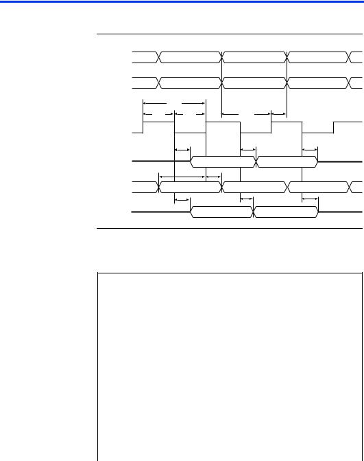
Figure 9 shows the timing requirements for the JTAG signals.
Figure 9. MAX 7000 JTAG Waveforms
TMS |
|
|
|
|
TDI |
|
|
|
|
tJCP |
|
|
|
|
tJCH |
t JCL |
tJPSU |
tJPH |
|
TCK |
|
|
|
|
tJPZX |
|
tJPCO |
|
tJPXZ |
TDO |
|
|
|
|
|
tJSSU |
tJSH |
|
|
Signal |
|
|
|
|
to Be |
|
|
|
|
Captured |
|
tJSCO |
t |
|
t |
|
JSXZ |
||
JSZX |
|
|
|
|
Signal
to Be
Driven
Table 12 shows the JTAG timing parameters and values for MAX 7000S devices.
Table 12. JTAG Timing Parameters & Values for MAX 7000S Devices
Symbol |
Parameter |
Min |
Max |
Unit |
|
|
|
|
|
tJCP |
TCK clock period |
100 |
|
ns |
tJCH |
TCK clock high time |
50 |
|
ns |
tJCL |
TCK clock low time |
50 |
|
ns |
tJPSU |
JTAG port setup time |
20 |
|
ns |
tJPH |
JTAG port hold time |
45 |
|
ns |
tJPCO |
JTAG port clock to output |
|
25 |
ns |
tJPZX |
JTAG port high impedance to valid output |
|
25 |
ns |
tJPXZ |
JTAG port valid output to high impedance |
|
25 |
ns |
tJSSU |
Capture register setup time |
20 |
|
ns |
tJSH |
Capture register hold time |
45 |
|
ns |
tJSCO |
Update register clock to output |
|
25 |
ns |
tJSZX |
Update register high impedance to valid output |
|
25 |
ns |
tJSXZ |
Update register valid output to high impedance |
|
25 |
ns |
f For more information, see Application Note 39 (IEEE 1149.1 (JTAG) Boundary-Scan Testing in Altera Devices).
24 |
Altera Corporation |