


MAX 7000 Programmable Logic Device Family Data Sheet
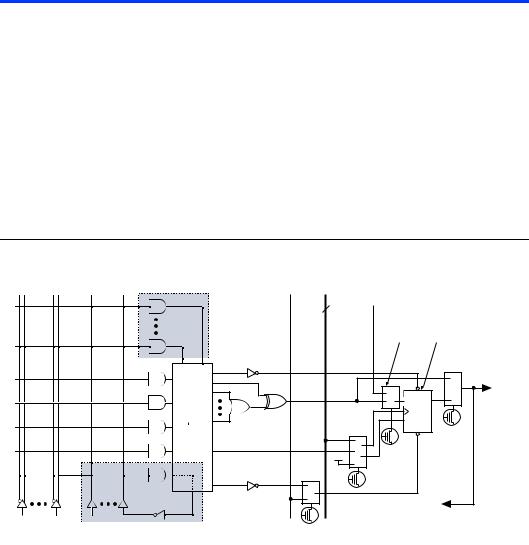
Figure 2 shows the architecture of MAX 7000E and MAX 7000S devices.
Figure 2. MAX 7000E & MAX 7000S Device Block Diagram
INPUT/GCLK1 |
|
|
|
|
|
|
|
|
INPUT/OE2/GCLK2 |
|
|
|
|
|
|
|
|
INPUT/OE1 |
|
|
|
|
|
|
|
|
INPUT/GCLRn |
|
|
|
|
|
|
|
|
|
|
6 Output Enables |
|
|
6 Output Enables |
|||
|
|
6 to16 |
LAB A |
|
|
LAB B |
6 to16 |
|
|
|
6 to16 |
36 |
|
36 |
Macrocells |
6 to16 |
|
|
I/O |
Macrocells |
|
|
I/O |
|||
6 to 16 I/O Pins |
Control |
|
1 to 16 |
|
|
17 to 32 |
|
Control |
|
Block |
|
|
|
|
|
|
Block |
|
|
|
16 |
|
16 |
|
|
|
|
6 |
|
6 to16 |
PIA |
6 to16 |
|
|
6 |
|
|
|
|
|
|
|
|
|
|
|
6 to16 |
LAB C |
|
|
LAB D |
6 to16 |
|
|
|
6 to16 |
36 |
|
36 |
Macrocells |
6 to16 |
|
|
I/O |
Macrocells |
|
|
I/O |
|||
6 to 16 I/O Pins |
|
33 to 48 |
|
|
49 to 64 |
|
||
Control |
|
|
|
|
Control |
|||
|
|
|
|
|
|
|
||
|
Block |
|
|
|
|
|
|
Block |
|
|
|
16 |
|
16 |
|
|
|
|
6 |
|
6 to16 |
|
6 to16 |
|
|
6 |
6 to 16 I/O Pins
6 to 16 I/O Pins
Logic Array Blocks
The MAX 7000 device architecture is based on the linking of highperformance, flexible, logic array modules called logic array blocks (LABs). LABs consist of 16-macrocell arrays, as shown in Figures 1 and 2. Multiple LABs are linked together via the programmable interconnect array (PIA), a global bus that is fed by all dedicated inputs, I/O pins, and macrocells.
8 |
Altera Corporation |
MAX 7000 Programmable Logic Device Family Data Sheet
Each LAB is fed by the following signals:
■36 signals from the PIA that are used for general logic inputs
■Global controls that are used for secondary register functions
■Direct input paths from I/O pins to the registers that are used for fast setup times for MAX 7000E and MAX 7000S devices
Macrocells
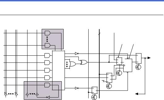
The MAX 7000 macrocell can be individually configured for either sequential or combinatorial logic operation. The macrocell consists of three functional blocks: the logic array, the product-term select matrix, and the programmable register. The macrocell of EPM7032, EPM7064, and EPM7096 devices is shown in Figure 3.
Figure 3. EPM7032, EPM7064 & EPM7096 Device Macrocell
|
Global |
Global |
|
|
|
Logic Array |
Clear |
Clocks |
|
|
|
|
|
|
|
|
From |
|
Parallel Logic |
2 |
|
|
I/O pin |
|
|
|
|
|
|
|
Expanders |
|
Fast Input |
Programmable |
|
|
(from other |
|
Select |
Register |
|
|
macrocells) |
|
|
|
|
|
|
|
|
Register |
|
|
|
|
|
Bypass |
|
|
To I/O |
|
Control |
PRN |
Block |
D/T |
Q |
Product- |
Clock/ |
|
|
Enable |
ENA |
||
Term |
|||
Select |
CLRN |
||
Select |
|||
|
|
||
Matrix |
|
|
|
|
VCC |
|
|
|
Clear |
|
|
|
Select |
|
|
|
Shared Logic |
to PIA |
|
|
|
||
|
Expanders |
|
36 Signals |
16 Expander |
from PIA |
Product Terms |
Altera Corporation |
9 |
MAX 7000 Programmable Logic Device Family Data Sheet
Figure 4 shows a MAX 7000E and MAX 7000S device macrocell.
Figure 4. MAX 7000E & MAX 7000S Device Macrocell
|
Global |
Global |
Logic Array |
Clear |
Clocks |
|
|
|
from |
2 |
|
|
I/O pin |
Parallel Logic |
|
|
|
Expanders |
Fast Input |
Programmable |
|
(from other |
Select |
Register |
|
macrocells) |
|
|
|
|
|
Register |
|
|
|
Bypass |
|
|
to I/O |
|
Control |
PRN |
Block |
D/T |
Q |
Product- |
Clock/ |
|
|
Enable |
ENA |
||
Term |
|||
Select |
CLRN |
||
Select |
|||
|
|
||
Matrix |
|
|
|
|
VCC |
|
|
|
Clear |
|
|
|
Select |
|
|
|
Shared Logic |
to PIA |
|
|
|
||
|
Expanders |
|
36 Signals |
16 Expander |
from PIA |
Product Terms |
|
|
Combinatorial logic is implemented in the logic array, which provides five product terms per macrocell. The product-term select matrix allocates these product terms for use as either primary logic inputs (to the OR and XOR gates) to implement combinatorial functions, or as secondary inputs to the macrocell’s register clear, preset, clock, and clock enable control functions. Two kinds of expander product terms (“expanders”) are available to supplement macrocell logic resources:
■Shareable expanders, which are inverted product terms that are fed back into the logic array
■Parallel expanders, which are product terms borrowed from adjacent macrocells
The Altera development system automatically optimizes product-term allocation according to the logic requirements of the design.
For registered functions, each macrocell flipflop can be individually programmed to implement D, T, JK, or SR operation with programmable clock control. The flipflop can be bypassed for combinatorial operation. During design entry, the designer specifies the desired flipflop type; the Altera development software then selects the most efficient flipflop operation for each registered function to optimize resource utilization.
10 |
Altera Corporation |