

FLEX 6000 Programmable Logic Device Family Data Sheet
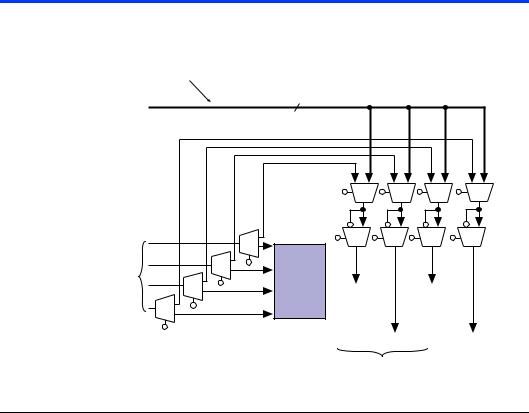
Figure 3. LAB Control Signals
The dedicated input signals can drive the clock and asynchronous clear signals.
Dedicated Inputs
Input signals to the first LE in an LAB (i.e., LE 1) can be rerouted to drive control signals within the LAB.
4 |
|
|
LE 1 |
|
|
LABCTRL1/ |
LABCTRL2 |
|
SYNCLR |
|
|
CLK1/SYNLOAD |
CLK2 |
|
LAB-wide control signals (SYNCLR and SYNLOAD
signals are used in counter mode).
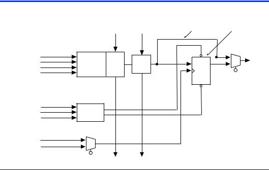
Logic Element
An LE, the smallest unit of logic in the FLEX 6000 architecture, has a compact size that provides efficient logic usage. Each LE contains a fourinput LUT, which is a function generator that can quickly implement any function of four variables. An LE contains a programmable flipflop, carry and cascade chains. Additionally, each LE drives both the local and the FastTrack Interconnect. See Figure 4.
8 |
Altera Corporation |
FLEX 6000 Programmable Logic Device Family Data Sheet
Figure 4. Logic Element
|
|
Carry-In |
Cascade-In |
Register Bypass |
Programmable |
||
|
|
|
|
Register |
|||
data1 |
Look-Up |
Carry |
Cascade |
|
PRN |
LE-Out |
|
data2 |
|
||||||
Table |
D |
Q |
|||||
data3 |
Chain |
Chain |
|
||||
(LUT) |
|
|
|
||||
|
|
|
|
|
|||
data4 |
|
|
|
|
|
|
|
|
|
|
|
CLRN |
|
||
labctrl1 |
Clear/ Preset |
|
|
|
|
|
|
labctrl2 |
|
|
|
|
|
||
Logic |
|
|
|
|
|
||
Chip-Wide Reset |
|
|
|
|
|
||
|
|
|
|
|
|
||
|
Clock |
|
|
|
|
|
|
|
Select |
|
|
|
|
|
|
labctrl3 |
|
|
|
|
|
|
|
labctrl4 |
|
|
|
|
|
|
|
|
|
Carry-Out |
Cascade-Out |
|
|
|
|
The programmable flipflop in the LE can be configured for D, T, JK, or SR operation. The clock and clear control signals on the flipflop can be driven by global signals, general-purpose I/O pins, or any internal logic. For combinatorial functions, the flipflop is bypassed and the output of the LUT drives the outputs of the LE. The LE output can drive both the local interconnect and the FastTrack Interconnect.
The FLEX 6000 architecture provides two types of dedicated high-speed data paths that connect adjacent LEs without using local interconnect paths: carry chains and cascade chains. A carry chain supports high-speed arithmetic functions such as counters and adders, while a cascade chain implements wide-input functions such as equivalent comparators with minimum delay. Carry and cascade chains connect LEs 2 through 10 in an LAB and all LABs in the same half of the row. Because extensive use of carry and cascade chains can reduce routing flexibility, these chains should be limited to speed-critical portions of a design.
Altera Corporation |
9 |

FLEX 6000 Programmable Logic Device Family Data Sheet
Carry Chain
The carry chain provides a very fast (0.1 ns) carry-forward function between LEs. The carry-in signal from a lower-order bit drives forward into the higher-order bit via the carry chain, and feeds into both the LUT and the next portion of the carry chain. This feature allows the FLEX 6000 architecture to implement high-speed counters, adders, and comparators of arbitrary width. Carry chain logic can be created automatically by the Altera software during design processing, or manually by the designer during design entry. Parameterized functions such as LPM and DesignWare functions automatically take advantage of carry chains for the appropriate functions.
Because the first LE of each LAB can generate control signals for that LAB, the first LE in each LAB is not included in carry chains. In addition, the inputs of the first LE in each LAB may be used to generate synchronous clear and load enable signals for counters implemented with carry chains.
Carry chains longer than nine LEs are implemented automatically by linking LABs together. For enhanced fitting, a long carry chain skips alternate LABs in a row. A carry chain longer than one LAB skips either from an even-numbered LAB to another even-numbered LAB, or from an odd-numbered LAB to another odd-numbered LAB. For example, the last LE of the first LAB in a row carries to the second LE of the third LAB in the row. In addition, the carry chain does not cross the middle of the row. For instance, in the EPF6016 device, the carry chain stops at the 11th LAB in a row and a new carry chain begins at the 12th LAB.
Figure 5 shows how an n-bit full adder can be implemented in n + 1 LEs with the carry chain. One portion of the LUT generates the sum of two bits using the input signals and the carry-in signal; the sum is routed to the output of the LE. Although the register can be bypassed for simple adders, it can be used for an accumulator function. Another portion of the LUT and the carry chain logic generates the carry-out signal, which is routed directly to the carry-in signal of the next-higher-order bit. The final carry-out signal is routed to an LE, where it is driven onto the FastTrack Interconnect.
10 |
Altera Corporation |
FLEX 6000 Programmable Logic Device Family Data Sheet
Figure 5. Carry Chain Operation
Carry-In
a1 |
LUT |
Register |
s1 |
|
|
|
|
b1 |
|
|
|
|
Carry Chain |
|
|
|
|
|
LE 2 |
a2 |
LUT |
Register |
s2 |
b2 |
|
|
|
|
Carry Chain |
|
|
|
|
|
LE 3 |
an |
|
|
|
|
|
|
|
|
|
sn |
|
|
|
|
LUT |
|
|
Register |
|
||
bn |
|
|
|
|
|
|
|
|
|
|
|
|
|
|
|
|
|
|
|
|
|
|
|
|
|
|
|
|
|
|
|
|
|
|
|
|
|
|
|
|
|
|
|
Carry Chain |
|
|
|
LE n + 1 |
|
LUT |
Register |
Carry-Out |
Carry Chain |
|
|
|
LE n + 2 |
|
Altera Corporation |
11 |