


FLEX 6000 Programmable Logic Device Family Data Sheet
Timing Model |
The continuous, high-performance FastTrack Interconnect routing |
|
resources ensure predictable performance and accurate simulation and |
|
timing analysis. This predictable performance contrasts with that of |
|
FPGAs, which use a segmented connection scheme and therefore have |
|
unpredictable performance. |
|
Device performance can be estimated by following the signal path from a |
|
source, through the interconnect, to the destination. For example, the |
|
registered performance between two LEs on the same row can be |
|
calculated by adding the following parameters: |
|
■ LE register clock-to-output delay (tCO + tREG_TO_OUT) |
|
■ Routing delay (tROW + tLOCAL) |
|
■ LE LUT delay (tDATA_TO_REG) |
|
■ LE register setup time (tSU) |
|
The routing delay depends on the placement of the source and destination |
|
LEs. A more complex registered path may involve multiple combinatorial |
|
LEs between the source and destination LEs. |
|
Timing simulation and delay prediction are available with the Simulator |
|
and Timing Analyzer, or with industry-standard EDA tools. The |
|
Simulator offers both pre-synthesis functional simulation to evaluate logic |
|
design accuracy and post-synthesis timing simulation with 0.1-ns |
|
resolution. The Timing Analyzer provides point-to-point timing delay |
|
information, setup and hold time analysis, and device-wide performance |
|
analysis. |
|
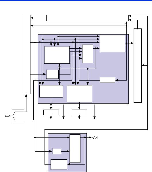
Figure 19 shows the overall timing model, which maps the possible |
|
routing paths to and from the various elements of the FLEX 6000 device. |
36 |
Altera Corporation |
FLEX 6000 Programmable Logic Device Family Data Sheet
Figure 19. FLEX 6000 Timing Model
tLOCAL
tDIN_D |
tDIN_C |
|
|
|
|
tROW |
|
||
Carry-In from |
Cascade-In from |
|
|
|
|||
Previous LE |
Previous LE |
|
|
|
|
||
|
|
|
|
|
|
|
tCASC_TO_OUT |
|
|
|
|
|
|
|
tCARRY_TO_OUT |
|
|
|
|
|
|
|
tDATA_TO_OUT |
t |
REG_TO_REG |
t |
SU |
tREG_TO_OUT |
|||
t |
tH |
|
|
||||
CASC_TO_REG |
|
|
|||||
t |
tCO |
|
|||||
CARRY_TO_REG |
|
||||||
t |
tCLR |
|
|||||
DATA_TO_REG |
|
||||||
|
|
|
|
|
|||
|
|
|
|
|
|
|
tCOL |
tC |
|
|
|
|
|
|
|
tLD_CLR |
|
|
|
|
|
||
|
|
|
|
|
|
|
tLEGLOBAL |
tCARRY_TO_CARRY |
t |
|
|
|
|||
tREG_TO_CARRY |
CARRY_TO_CASC |
|
|||||
tCASC_TO_CASC |
|
||||||
tDATA_TO_CARRY |
tREG_TO_CASC |
|
|
||||
|
|
|
|
tDATA_TO_CASC |
|
LE |
|
tLABCARRY |
|
tLABCASC |
|
|
|
||
Carry-out to |
Carry-out to |
Cascade-out Cascade-out |
|
||||
Next LE in |
Next LE in |
to Next LE in |
|
to Next LE in |
|
||
Same LAB |
Next LAB |
Same LAB |
|
Next LAB |
|
||
|
|
|
|
tOD1 |
|
I/O Pin |
|
|
|
|
|
tOD2 |
|
|
|
|
|
|
|
tOD3 |
|
|
|
|
|
tIOE |
tXZ |
|
|
|
|
|
|
tZX1 |
|
|
|
||
|
|
|
|
tZX2 |
|
|
|
|
|
|
|
tZX3 |
|
|
|
|
|
tIN |
|
|
|
|
|
|
|
tIN_DELAY |
IOE |
|
|
|
|
|
|
|
|
|
|
|
|
Altera Corporation |
37 |

FLEX 6000 Programmable Logic Device Family Data Sheet
Tables 19 through 21 describe the FLEX 6000 internal timing microparameters, which are expressed as worst-case values. Using hand calculations, these parameters can be used to estimate design performance. However, before committing designs to silicon, actual worst-case performance should be modeled using timing simulation and timing analysis. Tables 22 and 23 describe FLEX 6000 external timing parameters.
Table 19. LE Timing Microparameters |
Note (1) |
|
|
|
|
|
|
Symbol |
|
Parameter |
Conditions |
|
|
|
|
tREG_TO_REG |
LUT delay for LE register feedback in carry chain |
|
|
tCASC_TO_REG |
Cascade-in to register delay |
|
|
tCARRY_TO_REG |
Carry-in to register delay |
|
|
tDATA_TO_REG |
LE input to register delay |
|
|
tCASC_TO_OUT |
Cascade-in to LE output delay |
|
|
tCARRY_TO_OUT |
Carry-in to LE output delay |
|
|
tDATA_TO_OUT |
LE input to LE output delay |
|
|
tREG_TO_OUT |
Register output to LE output delay |
|
|
tSU |
LE register setup time before clock; LE register recovery time after |
|
|
|
asynchronous clear |
|
|
|
|
|
|
tH |
LE register hold time after clock |
|
|
tCO |
LE register clock-to-output delay |
|
|
tCLR |
LE register clear delay |
|
|
tC |
LE register control signal delay |
|
|
tLD_CLR |
Synchronous load or clear delay in counter mode |
|
|
tCARRY_TO_CARRY |
Carry-in to carry-out delay |
|
|
tREG_TO_CARRY |
Register output to carry-out delay |
|
|
tDATA_TO_CARRY |
LE input to carry-out delay |
|
|
tCARRY_TO_CASC |
Carry-in to cascade-out delay |
|
|
tCASC_TO_CASC |
Cascade-in to cascade-out delay |
|
|
tREG_TO_CASC |
Register-out to cascade-out delay |
|
|
tDATA_TO_CASC |
LE input to cascade-out delay |
|
|
tCH |
LE register clock high time |
|
|
tCL |
LE register clock low time |
|
|
38 |
Altera Corporation |

FLEX 6000 Programmable Logic Device Family Data Sheet
Table 20. IOE Timing Microparameters |
Note (1) |
|
|
|
|
|
|
|
|
|
|
Symbol |
|
Parameter |
|
Conditions |
|
|
|
|
|
||
tOD1 |
Output buffer and pad delay, slow slew rate = off, VCCIO = VCCINT |
C1 |
= 35 pF (2) |
||
tOD2 |
Output buffer and pad delay, slow slew rate = off, VCCIO = low voltage |
C1 |
= 35 pF (3) |
||
tOD3 |
Output buffer and pad delay, slow slew rate = on |
C1 |
= 35 pF (4) |
||
tXZ |
Output buffer disable delay |
|
|
C1 |
= 5 pF |
tZX1 |
Output buffer enable delay, slow slew rate = off, VCCIO = VCCINT |
C1 |
= 35 pF (2) |
||
tZX2 |
Output buffer enable delay, slow slew rate = off, VCCIO = low voltage |
C1 |
= 35 pF (3) |
||
tZX3 |
IOE output buffer enable delay, slow slew rate = on |
C1 |
= 35 pF (4) |
||
tIOE |
Output enable control delay |
|
|
|
|
tIN |
Input pad and buffer to FastTrack Interconnect delay |
|
|
||
tIN_DELAY |
Input pad and buffer to FastTrack Interconnect delay with additional delay |
|
|
||
|
turned on |
|
|
|
|
|
|
|
|
|
|
|
|
|
|
||
Table 21. Interconnect Timing Microparameters |
Note (1) |
|
|
||
|
|
|
|
|
|
Symbol |
|
Parameter |
|
Conditions |
|
|
|
|
|
|
|
tLOCAL |
LAB local interconnect delay |
|
|
|
|
tROW |
Row interconnect routing delay |
|
(5) |
|
|
tCOL |
Column interconnect routing delay |
|
(5) |
|
|
tDIN_D |
Dedicated input to LE data delay |
|
(5) |
|
|
tDIN_C |
Dedicated input to LE control delay |
|
|
|
|
tLEGLOBAL |
LE output to LE control via internally-generated global signal delay |
(5) |
|
||
tLABCARRY |
Routing delay for the carry-out of an LE driving the carry-in signal of a |
|
|
||
|
different LE in a different LAB |
|
|
|
|
|
|
|
|
||
tLABCASC |
Routing delay for the cascade-out signal of an LE driving the cascade-in |
|
|
||
|
signal of a different LE in a different LAB |
|
|
||
|
|
|
|
|
|
|
|
|
|
||
Table 22. External Reference Timing Parameters |
|
|
|
||
|
|
|
|
|
|
Symbol |
|
Parameter |
|
Conditions |
|
|
|
|
|
|
|
t1 |
Register-to-register test pattern |
|
(6) |
|
|
tDRR |
Register-to-register delay via 4 LEs, 3 row interconnects, and 4 local |
(7) |
|
||
|
interconnects |
|
|
|
|
|
|
|
|
|
|
Altera Corporation |
39 |
FLEX 6000 Programmable Logic Device Family Data Sheet
Table 23. External Timing Parameters
Symbol |
Parameter |
Conditions |
|
|
|
tINSU |
Setup time with global clock at LE register |
(8) |
tINH |
Hold time with global clock at LE register |
(8) |
tOUTCO |
Clock-to-output delay with global clock with LE register using FastFLEX I/O |
(8) |
|
pin |
|
|
|
|
Notes to tables:
(1)Microparameters are timing delays contributed by individual architectural elements and cannot be measured explicitly.
(2)Operating conditions:
VCCIO = 5.0 V ± 5% for commercial use in 5.0-V FLEX 6000 devices. VCCIO = 5.0 V ± 10% for industrial use in 5.0-V FLEX 6000 devices.
VCCIO = 3.3 V ± 10% for commercial or industrial use in 3.3-V FLEX 6000 devices.
(3)Operating conditions:
VCCIO = 3.3 V ± 10% for commercial or industrial use in 5.0-V FLEX 6000 devices. VCCIO = 2.5 V ± 0.2 V for commercial or industrial use in 3.3-V FLEX 6000 devices.
(4)Operating conditions:
VCCIO = 2.5 V, 3.3 V, or 5.0 V.
(5)These parameters are worst-case values for typical applications. Post-compilation timing simulation and timing analysis are required to determine actual worst-case performance.
(6)This timing parameter shows the delay of a register-to-register test pattern and is used to determine speed grades. There are 12 LEs, including source and destination registers. The row and column interconnects between the registers vary in length.
(7)This timing parameter is shown for reference and is specified by characterization.
(8)This timing parameter is specified by characterization.
Tables 24 through 28 show the timing information for EPF6010A and
EPF6016A devices.
Table 24. LE Timing Microparameters for EPF6010A & EPF6016A Devices |
(Part 1 of 2) |
|
|||||||||
|
|
|
|
|
|
|
|
|
|
|
|
Parameter |
|
|
|
Speed Grade |
|
|
|
Unit |
|||
|
|
|
|
|
|
|
|
|
|
|
|
|
-1 |
|
|
-2 |
|
|
-3 |
|
|||
|
|
|
|
|
|
|
|
|
|
|
|
|
Min |
|
Max |
Min |
|
Max |
|
Min |
|
Max |
|
|
|
|
|
|
|
|
|
|
|
|
|
tREG_TO_REG |
|
|
1.2 |
|
|
1.3 |
|
|
|
1.7 |
ns |
tCASC_TO_REG |
|
|
0.9 |
|
|
1.0 |
|
|
|
1.2 |
ns |
tCARRY_TO_REG |
|
|
0.9 |
|
|
1.0 |
|
|
|
1.2 |
ns |
tDATA_TO_REG |
|
|
1.1 |
|
|
1.2 |
|
|
|
1.5 |
ns |
tCASC_TO_OUT |
|
|
1.3 |
|
|
1.4 |
|
|
|
1.8 |
ns |
tCARRY_TO_OUT |
|
|
1.6 |
|
|
1.8 |
|
|
|
2.3 |
ns |
tDATA_TO_OUT |
|
|
1.7 |
|
|
2.0 |
|
|
|
2.5 |
ns |
tREG_TO_OUT |
|
|
0.4 |
|
|
0.4 |
|
|
|
0.5 |
ns |
tSU |
0.9 |
|
|
1.0 |
|
|
|
1.3 |
|
|
ns |
tH |
1.4 |
|
|
1.7 |
|
|
|
2.1 |
|
|
ns |
40 |
Altera Corporation |
FLEX 6000 Programmable Logic Device Family Data Sheet
Table 24. LE Timing Microparameters for EPF6010A & EPF6016A Devices |
(Part 2 of 2) |
|
|||||||||
|
|
|
|
|
|
|
|
|
|
|
|
Parameter |
|
|
|
Speed Grade |
|
|
|
Unit |
|||
|
|
|
|
|
|
|
|
|
|
|
|
|
-1 |
|
|
-2 |
|
|
-3 |
|
|||
|
|
|
|
|
|
|
|
|
|
|
|
|
Min |
|
Max |
Min |
|
Max |
|
Min |
|
Max |
|
|
|
|
|
|
|
|
|
|
|
|
|
tCO |
|
|
0.3 |
|
|
0.4 |
|
|
|
0.4 |
ns |
tCLR |
|
|
0.4 |
|
|
0.4 |
|
|
|
0.5 |
ns |
tC |
|
|
1.8 |
|
|
2.1 |
|
|
|
2.6 |
ns |
tLD_CLR |
|
|
1.8 |
|
|
2.1 |
|
|
|
2.6 |
ns |
tCARRY_TO_CARRY |
|
|
0.1 |
|
|
0.1 |
|
|
|
0.1 |
ns |
tREG_TO_CARRY |
|
|
1.6 |
|
|
1.9 |
|
|
|
2.3 |
ns |
tDATA_TO_CARRY |
|
|
2.1 |
|
|
2.5 |
|
|
|
3.0 |
ns |
tCARRY_TO_CASC |
|
|
1.0 |
|
|
1.1 |
|
|
|
1.4 |
ns |
tCASC_TO_CASC |
|
|
0.5 |
|
|
0.6 |
|
|
|
0.7 |
ns |
tREG_TO_CASC |
|
|
1.4 |
|
|
1.7 |
|
|
|
2.1 |
ns |
tDATA_TO_CASC |
|
|
1.1 |
|
|
1.2 |
|
|
|
1.5 |
ns |
tCH |
2.5 |
|
|
3.0 |
|
|
|
3.5 |
|
|
ns |
tCL |
2.5 |
|
|
3.0 |
|
|
|
3.5 |
|
|
ns |
|
|
|
|
||||||||
Table 25. IOE Timing Microparameters for EPF6010A & EPF6016A Devices |
|
|
|
||||||||
|
|
|
|
|
|
|
|
|
|||
Parameter |
|
|
|
Speed Grade |
|
|
|
Unit |
|||
|
|
|
|
|
|
|
|
|
|||
|
-1 |
|
|
-2 |
|
|
-3 |
|
|||
|
|
|
|
|
|
|
|
|
|
|
|
|
Min |
|
Max |
Min |
|
Max |
|
Min |
|
Max |
|
|
|
|
|
|
|
|
|
|
|
|
|
tOD1 |
|
|
1.9 |
|
|
2.2 |
|
|
|
2.7 |
ns |
tOD2 |
|
|
4.1 |
|
|
4.8 |
|
|
|
5.8 |
ns |
tOD3 |
|
|
5.8 |
|
|
6.8 |
|
|
|
8.3 |
ns |
tXZ |
|
|
1.4 |
|
|
1.7 |
|
|
|
2.1 |
ns |
tXZ1 |
|
|
1.4 |
|
|
1.7 |
|
|
|
2.1 |
ns |
tXZ2 |
|
|
3.6 |
|
|
4.3 |
|
|
|
5.2 |
ns |
tXZ3 |
|
|
5.3 |
|
|
6.3 |
|
|
|
7.7 |
ns |
tIOE |
|
|
0.5 |
|
|
0.6 |
|
|
|
0.7 |
ns |
tIN |
|
|
3.6 |
|
|
4.1 |
|
|
|
5.1 |
ns |
tIN_DELAY |
|
|
4.8 |
|
|
5.4 |
|
|
|
6.7 |
ns |
Altera Corporation |
41 |

FLEX 6000 Programmable Logic Device Family Data Sheet
Table 26. Interconnect Timing Microparameters for EPF6010A & EPF6016A Devices
Parameter |
|
|
|
|
|
|
|
Speed Grade |
|
|
|
|
|
Unit |
||||||
|
|
|
|
|
|
|
|
|
|
|
|
|
|
|
|
|
|
|
|
|
|
|
-1 |
|
|
|
-2 |
|
|
|
|
-3 |
|
|
|
|
|||||
|
|
|
|
|
|
|
|
|
|
|
|
|
|
|
|
|
|
|
|
|
|
|
Min |
|
Max |
|
Min |
|
|
Max |
|
|
Min |
|
|
Max |
|
|
|||
|
|
|
|
|
|
|
|
|
|
|
|
|
|
|
|
|
|
|
|
|
tLOCAL |
|
|
|
|
0.7 |
|
|
|
|
0.7 |
|
|
|
|
|
1.0 |
|
ns |
||
tROW |
|
|
|
|
2.9 |
|
|
|
|
3.2 |
|
|
|
|
|
3.2 |
|
ns |
||
tCOL |
|
|
|
|
1.2 |
|
|
|
|
1.3 |
|
|
|
|
|
1.4 |
|
ns |
||
tDIN_D |
|
|
|
|
5.4 |
|
|
|
|
5.7 |
|
|
|
|
|
6.4 |
|
ns |
||
tDIN_C |
|
|
|
|
4.3 |
|
|
|
|
5.0 |
|
|
|
|
|
6.1 |
|
ns |
||
tLEGLOBAL |
|
|
|
|
2.6 |
|
|
|
|
3.0 |
|
|
|
|
|
3.7 |
|
ns |
||
tLABCARRY |
|
|
|
|
0.7 |
|
|
|
|
0.8 |
|
|
|
|
|
0.9 |
|
ns |
||
tLABCASC |
|
|
|
|
1.3 |
|
|
|
|
1.4 |
|
|
|
|
|
1.8 |
|
ns |
||
|
|
|
|
|
|
|
|
|
|
|
||||||||||
Table 27. External Reference Timing Parameters for EPF6010A & EPF6016A Devices |
|
|
|
|||||||||||||||||
|
|
|
|
|
|
|
|
|
|
|
|
|
|
|
|
|||||
Parameter |
Device |
|
|
|
|
|
|
Speed Grade |
|
|
|
|
|
Unit |
||||||
|
|
|
|
|
|
|
|
|
|
|
|
|
|
|
|
|
|
|
||
|
|
|
|
|
-1 |
|
|
|
|
-2 |
|
|
-3 |
|
|
|
||||
|
|
|
|
|
|
|
|
|
|
|
|
|
|
|
|
|||||
|
|
|
Min |
|
Max |
|
Min |
|
Max |
|
Min |
|
Max |
|
|
|||||
|
|
|
|
|
|
|
|
|
|
|
|
|
|
|
|
|
|
|||
t1 |
EPF6010A |
|
|
|
37.6 |
|
|
|
|
43.6 |
|
|
|
|
|
53.7 |
|
ns |
||
|
EPF6016A |
|
|
|
38.0 |
|
|
|
|
44.0 |
|
|
|
|
|
54.1 |
|
ns |
||
|
|
|
|
|
|
|
|
|
|
|
|
|
||||||||
|
|
|
|
|
|
|
||||||||||||||
Table 28. External Timing Parameters for EPF6010A & EPF6016A Devices |
|
|
|
|
|
|
||||||||||||||
|
|
|
|
|
|
|
|
|
|
|
|
|||||||||
Parameter |
|
|
|
|
|
|
|
Speed Grade |
|
|
|
|
|
Unit |
||||||
|
|
|
|
|
|
|
|
|
|
|
|
|
|
|
|
|||||
|
|
-1 |
|
|
|
-2 |
|
|
|
|
-3 |
|
|
|
|
|||||
|
|
|
|
|
|
|
|
|
|
|
|
|
||||||||
|
|
Min |
|
Max |
|
Min |
|
|
Max |
|
|
Min |
|
|
Max |
|
|
|||
|
|
|
|
|
|
|
|
|
|
|
|
|
|
|
|
|
|
|
||
tINSU |
|
2.1 (1) |
|
|
|
|
2.4 (1) |
|
|
|
|
|
3.3 (1) |
|
|
|
|
ns |
||
tINH |
|
0.2 (2) |
|
|
|
|
0.3 (2) |
|
|
|
|
|
0.1 (2) |
|
|
|
|
ns |
||
tOUTCO |
|
2.0 |
|
7.1 |
|
2.0 |
|
8.2 |
|
|
2.0 |
|
|
10.1 |
|
ns |
||||
Notes:
(1)Setup times are longer when the Increase Input Delay option is turned on. The setup time values are shown with the
Increase Input Delay option turned off.
(2)Hold time is zero when the Increase Input Delay option is turned on.
42 |
Altera Corporation |

FLEX 6000 Programmable Logic Device Family Data Sheet
Tables 29 through 33 show the timing information for EPF6016 devices.
Table 29. LE Timing Microparameters for EPF6016 Devices
Parameter |
|
|
Speed Grade |
|
|
Unit |
||
|
|
|
|
|
|
|
|
|
|
|
-2 |
|
|
-3 |
|
||
|
|
|
|
|
|
|
|
|
|
Min |
|
Max |
|
Min |
|
Max |
|
|
|
|
|
|
|
|
|
|
tREG_TO_REG |
|
|
2.2 |
|
|
|
2.8 |
ns |
tCASC_TO_REG |
|
|
0.9 |
|
|
|
1.2 |
ns |
tCARRY_TO_REG |
|
|
1.6 |
|
|
|
2.1 |
ns |
tDATA_TO_REG |
|
|
2.4 |
|
|
|
3.0 |
ns |
tCASC_TO_OUT |
|
|
1.3 |
|
|
|
1.7 |
ns |
tCARRY_TO_OUT |
|
|
2.4 |
|
|
|
3.0 |
ns |
tDATA_TO_OUT |
|
|
2.7 |
|
|
|
3.4 |
ns |
tREG_TO_OUT |
|
|
0.3 |
|
|
|
0.5 |
ns |
tSU |
1.1 |
|
|
|
1.6 |
|
|
ns |
tH |
1.8 |
|
|
|
2.3 |
|
|
ns |
tCO |
|
|
0.3 |
|
|
|
0.4 |
ns |
tCLR |
|
|
0.5 |
|
|
|
0.6 |
ns |
tC |
|
|
1.2 |
|
|
|
1.5 |
ns |
tLD_CLR |
|
|
1.2 |
|
|
|
1.5 |
ns |
tCARRY_TO_CARRY |
|
|
0.2 |
|
|
|
0.4 |
ns |
tREG_TO_CARRY |
|
|
0.8 |
|
|
|
1.1 |
ns |
tDATA_TO_CARRY |
|
|
1.7 |
|
|
|
2.2 |
ns |
tCARRY_TO_CASC |
|
|
1.7 |
|
|
|
2.2 |
ns |
tCASC_TO_CASC |
|
|
0.9 |
|
|
|
1.2 |
ns |
tREG_TO_CASC |
|
|
1.6 |
|
|
|
2.0 |
ns |
tDATA_TO_CASC |
|
|
1.7 |
|
|
|
2.1 |
ns |
tCH |
4.0 |
|
|
|
4.0 |
|
|
ns |
tCL |
4.0 |
|
|
|
4.0 |
|
|
ns |
|
|
|
|
|
||||
Table 30. IOE Timing Microparameters for EPF6016 Devices |
|
|
|
|
||||
|
|
|
|
|
|
|
||
Parameter |
|
|
Speed Grade |
|
|
Unit |
||
|
|
|
|
|
|
|
||
|
|
-2 |
|
|
-3 |
|
||
|
|
|
|
|
|
|
|
|
|
Min |
|
Max |
|
Min |
|
Max |
|
|
|
|
|
|
|
|
|
|
tOD1 |
|
|
2.3 |
|
|
|
2.8 |
ns |
tOD2 |
|
|
4.6 |
|
|
|
5.1 |
ns |
Altera Corporation |
43 |

FLEX 6000 Programmable Logic Device Family Data Sheet
Table 30. IOE Timing Microparameters for EPF6016 Devices
Parameter |
|
|
Speed Grade |
|
|
Unit |
|
|
|
|
|
|
|
|
|
|
|
-2 |
|
-3 |
|
||
|
|
|
|
|
|
|
|
|
Min |
|
Max |
Min |
|
Max |
|
|
|
|
|
|
|
|
|
tOD3 |
|
|
4.7 |
|
|
5.2 |
ns |
tXZ |
|
|
2.3 |
|
|
2.8 |
ns |
tZX1 |
|
|
2.3 |
|
|
2.8 |
ns |
tZX2 |
|
|
4.6 |
|
|
5.1 |
ns |
tZX3 |
|
|
4.7 |
|
|
5.2 |
ns |
tIOE |
|
|
0.5 |
|
|
0.6 |
ns |
tIN |
|
|
3.3 |
|
|
4.0 |
ns |
tIN_DELAY |
|
|
4.6 |
|
|
5.6 |
ns |
|
|
|
|
||||
Table 31. Interconnect Timing Microparameters for EPF6016 Devices |
|
|
|
||||
|
|
|
|
|
|
||
Parameter |
|
|
Speed Grade |
|
|
Unit |
|
|
|
|
|
|
|
||
|
|
-2 |
|
-3 |
|
||
|
|
|
|
|
|
|
|
|
Min |
|
Max |
Min |
|
Max |
|
|
|
|
|
|
|
|
|
tLOCAL |
|
|
0.8 |
|
|
1.0 |
ns |
tROW |
|
|
2.9 |
|
|
3.3 |
ns |
tCOL |
|
|
2.3 |
|
|
2.5 |
ns |
tDIN_D |
|
|
4.9 |
|
|
6.0 |
ns |
tDIN_C |
|
|
4.8 |
|
|
6.0 |
ns |
tLEGLOBAL |
|
|
3.1 |
|
|
3.9 |
ns |
tLABCARRY |
|
|
0.4 |
|
|
0.5 |
ns |
tLABCASC |
|
|
0.8 |
|
|
1.0 |
ns |
|
|
|
|
||||
Table 32. External Reference Timing Parameters for EPF6016 Devices |
|
|
|
||||
|
|
|
|
|
|
||
Parameter |
|
|
Speed Grade |
|
|
Unit |
|
|
|
|
|
|
|
||
|
|
-2 |
|
-3 |
|
||
|
|
|
|
|
|
|
|
|
Min |
|
Max |
Min |
|
Max |
|
|
|
|
|
|
|
|
|
t1 |
|
|
53.0 |
|
|
65.0 |
ns |
tDRR |
|
|
16.0 |
|
|
20.0 |
ns |
44 |
Altera Corporation |

FLEX 6000 Programmable Logic Device Family Data Sheet
Table 33. External Timing Parameters for EPF6016 Devices
|
Parameter |
|
|
Speed Grade |
|
|
Unit |
|
|
|
|
|
|
|
|
|
|
|
|
-2 |
|
|
-3 |
|
||
|
|
|
|
|
|
|
|
|
|
|
Min |
|
Max |
Min |
|
Max |
|
|
|
|
|
|
|
|
|
|
tINSU |
|
3.2 |
|
|
4.1 |
|
|
ns |
tINH |
|
0.0 |
|
|
0.0 |
|
|
ns |
tOUTCO |
|
2.0 |
|
7.9 |
2.0 |
|
9.9 |
ns |
Tables 34 through 38 show the timing information for EPF6024A devices.
Table 34. LE Timing Microparameters for EPF6024A Devices
Parameter |
|
|
|
Speed Grade |
|
|
|
Unit |
||
|
|
|
|
|
|
|
|
|
|
|
|
-1 |
|
|
-2 |
|
-3 |
|
|||
|
|
|
|
|
|
|
|
|
|
|
|
Min |
|
Max |
Min |
|
Max |
Min |
|
Max |
|
|
|
|
|
|
|
|
|
|
|
|
tREG_TO_REG |
|
|
1.2 |
|
|
1.3 |
|
|
1.6 |
ns |
tCASC_TO_REG |
|
|
0.7 |
|
|
0.8 |
|
|
1.0 |
ns |
tCARRY_TO_REG |
|
|
1.6 |
|
|
1.8 |
|
|
2.2 |
ns |
tDATA_TO_REG |
|
|
1.3 |
|
|
1.4 |
|
|
1.7 |
ns |
tCASC_TO_OUT |
|
|
1.2 |
|
|
1.3 |
|
|
1.6 |
ns |
tCARRY_TO_OUT |
|
|
2.0 |
|
|
2.2 |
|
|
2.6 |
ns |
tDATA_TO_OUT |
|
|
1.8 |
|
|
2.1 |
|
|
2.6 |
ns |
tREG_TO_OUT |
|
|
0.3 |
|
|
0.3 |
|
|
0.4 |
ns |
tSU |
0.9 |
|
|
1.0 |
|
|
1.2 |
|
|
ns |
tH |
1.3 |
|
|
1.4 |
|
|
1.7 |
|
|
ns |
tCO |
|
|
0.2 |
|
|
0.3 |
|
|
0.3 |
ns |
tCLR |
|
|
0.3 |
|
|
0.3 |
|
|
0.4 |
ns |
tC |
|
|
1.9 |
|
|
2.1 |
|
|
2.5 |
ns |
tLD_CLR |
|
|
1.9 |
|
|
2.1 |
|
|
2.5 |
ns |
tCARRY_TO_CARRY |
|
|
0.2 |
|
|
0.2 |
|
|
0.3 |
ns |
tREG_TO_CARRY |
|
|
1.4 |
|
|
1.6 |
|
|
1.9 |
ns |
tDATA_TO_CARRY |
|
|
1.3 |
|
|
1.4 |
|
|
1.7 |
ns |
tCARRY_TO_CASC |
|
|
1.1 |
|
|
1.2 |
|
|
1.4 |
ns |
tCASC_TO_CASC |
|
|
0.7 |
|
|
0.8 |
|
|
1.0 |
ns |
tREG_TO_CASC |
|
|
1.4 |
|
|
1.6 |
|
|
1.9 |
ns |
tDATA_TO_CASC |
|
|
1.0 |
|
|
1.1 |
|
|
1.3 |
ns |
tCH |
2.5 |
|
|
3.0 |
|
|
3.5 |
|
|
ns |
tCL |
2.5 |
|
|
3.0 |
|
|
3.5 |
|
|
ns |
Altera Corporation |
45 |

FLEX 6000 Programmable Logic Device Family Data Sheet
Table 35. IOE Timing Microparameters for EPF6024A Devices
Parameter |
|
|
|
Speed Grade |
|
|
|
Unit |
|||
|
|
|
|
|
|
|
|
|
|
|
|
|
-1 |
|
|
-2 |
|
|
-3 |
|
|||
|
|
|
|
|
|
|
|
|
|
|
|
|
Min |
|
Max |
Min |
|
Max |
|
Min |
|
Max |
|
|
|
|
|
|
|
|
|
|
|
|
|
tOD1 |
|
|
1.9 |
|
|
2.1 |
|
|
|
2.5 |
ns |
tOD2 |
|
|
4.0 |
|
|
4.4 |
|
|
|
5.3 |
ns |
tOD3 |
|
|
7.0 |
|
|
7.8 |
|
|
|
9.3 |
ns |
tXZ |
|
|
4.3 |
|
|
4.8 |
|
|
|
5.8 |
ns |
tXZ1 |
|
|
4.3 |
|
|
4.8 |
|
|
|
5.8 |
ns |
tXZ2 |
|
|
6.4 |
|
|
7.1 |
|
|
|
8.6 |
ns |
tXZ3 |
|
|
9.4 |
|
|
10.5 |
|
|
|
12.6 |
ns |
tIOE |
|
|
0.5 |
|
|
0.6 |
|
|
|
0.7 |
ns |
tIN |
|
|
3.3 |
|
|
3.7 |
|
|
|
4.4 |
ns |
tIN_DELAY |
|
|
5.3 |
|
|
5.9 |
|
|
|
7.0 |
ns |
|
|
|
|
|
|||||||
Table 36. Interconnect Timing Microparameters for EPF6024A Devices |
|
|
|
|
|||||||
|
|
|
|
|
|
|
|||||
Parameter |
|
|
|
Speed Grade |
|
|
|
Unit |
|||
|
|
|
|
|
|
|
|
|
|||
|
-1 |
|
|
-2 |
|
|
-3 |
|
|||
|
|
|
|
|
|
|
|
|
|
|
|
|
Min |
|
Max |
Min |
|
Max |
|
Min |
|
Max |
|
|
|
|
|
|
|
|
|
|
|
|
|
tLOCAL |
|
|
0.8 |
|
|
0.8 |
|
|
|
1.1 |
ns |
tROW |
|
|
3.0 |
|
|
3.1 |
|
|
|
3.3 |
ns |
tCOL |
|
|
3.0 |
|
|
3.2 |
|
|
|
3.4 |
ns |
tDIN_D |
|
|
5.4 |
|
|
5.6 |
|
|
|
6.2 |
ns |
tDIN_C |
|
|
4.6 |
|
|
5.1 |
|
|
|
6.1 |
ns |
tLEGLOBAL |
|
|
3.1 |
|
|
3.5 |
|
|
|
4.3 |
ns |
tLABCARRY |
|
|
0.6 |
|
|
0.7 |
|
|
|
0.8 |
ns |
tLABCASC |
|
|
0.3 |
|
|
0.3 |
|
|
|
0.4 |
ns |
|
|
|
|
|
|||||||
Table 37. External Reference Timing Parameters for EPF6024A Devices |
|
|
|
|
|||||||
|
|
|
|
|
|
|
|||||
Parameter |
|
|
|
Speed Grade |
|
|
|
Unit |
|||
|
|
|
|
|
|
|
|
|
|||
|
-1 |
|
|
-2 |
|
|
-3 |
|
|||
|
|
|
|
|
|
|
|
|
|
|
|
|
Min |
|
Max |
Min |
|
Max |
|
Min |
|
Max |
|
|
|
|
|
|
|
|
|
|
|
|
|
t1 |
|
|
45.0 |
|
|
50.0 |
|
|
|
60.0 |
ns |
46 |
Altera Corporation |

FLEX 6000 Programmable Logic Device Family Data Sheet
Table 38. External Timing Parameters for EPF6024A Devices
Parameter |
|
|
|
Speed Grade |
|
|
|
Unit |
||
|
|
|
|
|
|
|
|
|
|
|
|
|
-1 |
|
-2 |
|
-3 |
|
|||
|
|
|
|
|
|
|
|
|
|
|
|
Min |
|
Max |
Min |
|
Max |
Min |
|
Max |
|
|
|
|
|
|
|
|
|
|
|
|
tINSU |
2.0 (1) |
|
|
2.2 (1) |
|
|
2.6 (1) |
|
|
ns |
tINH |
0.2 (2) |
|
|
0.2 (2) |
|
|
0.3 (2) |
|
|
ns |
tOUTCO |
2.0 |
|
7.4 |
2.0 |
|
8.2 |
2.0 |
|
9.9 |
ns |
Notes:
(1)Setup times are longer when the Increase Input Delay option is turned on. The setup time values are shown with the
Increase Input Delay option turned off.
(2)Hold time is zero when the Increase Input Delay option is turned on.
Power
Consumption
The supply power (P) for FLEX 6000 devices can be calculated with the following equations:
P |
= |
PINT + PIO |
P |
= |
(ICCSTANDBY + ICCACTIVE) × VCC + PIO |
Typical ICCSTANDBY values are shown as ICC0 in the “FLEX 6000 Device DC Operating Conditions” table on pages 31 and 33 of this data sheet. The
ICCACTIVE value depends on the switching frequency and the application logic. This value is based on the amount of current that each LE typically
consumes. The PIO value, which depends on the device output load characteristics and switching frequency, can be calculated using the guidelines given in Application Note 74 (Evaluating Power for Altera Devices).
The ICCACTIVE value can be calculated with the following equation:
ICCACTIVE = K × fMAX × N × togLC × |
|
µA |
||
---------------------------- |
||||
MHz × LE |
||||
Where: |
|
|
|
|
fMAX |
= |
Maximum operating frequency in MHz |
||
N |
= |
Total number of LEs used in a FLEX 6000 device |
||
togLC |
= |
Average percentage of LEs toggling at each clock |
||
|
|
(typically 12.5%) |
|
|
K |
= |
Constant, shown in Table 39 |
||
|
|
|
||
Table 39. K Constant Values |
|
|
||
|
|
|
|
|
|
|
Device |
|
K Value |
|
|
|
|
|
|
|
EPF6010A |
|
14 |
|
|
|
|
|
|
|
EPF6016 |
|
88 |
|
|
|
|
|
|
|
EPF6016A |
|
14 |
|
|
|
|
|
|
|
EPF6024A |
|
14 |
|
|
|
|
|
Altera Corporation |
47 |

FLEX 6000 Programmable Logic Device Family Data Sheet
This calculation provides an ICC estimate based on typical conditions with no output load. The actual ICC should be verified during operation because this measurement is sensitive to the actual pattern in the device and the environmental operating conditions.
To better reflect actual designs, the power model (and the constant K in the power calculation equations shown above) for continuous interconnect FLEX devices assumes that LEs drive FastTrack Interconnect channels. In contrast, the power model of segmented FPGAs assumes that all LEs drive only one short interconnect segment. This assumption may lead to inaccurate results, compared to measured power consumption for an actual design in a segmented interconnect FPGA.
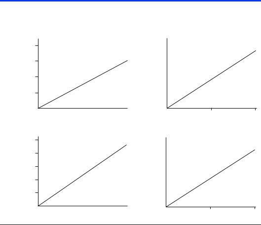
Figure 20 shows the relationship between the current and operating frequency for EPF6010A, EPF6016, EPF6016A, and EPF6024A devices.
48 |
Altera Corporation |
FLEX 6000 Programmable Logic Device Family Data Sheet
Figure 20. ICCACTIVE vs. Operating Frequency
EPF6010A
200
150
ICC Supply
Current
(mA) 100
50
0
EPF6016A
250
200
ICC Supply 150 Current
(mA)
100
50
0
|
|
|
|
EPF6016 |
|
|
|
|
|
|
|
|
|
|
1000 |
|
|
|
|
|
|
|
|
|
|
|
|
|
|
|
|
|
|
|
800 |
|
|
|
|
|
|
|
|
|
|
|
|
|
|
|
|
|
|
ICC Supply 600 |
|
|
|||
|
|
|
|
|
|
||||
|
|
|
|
Current |
|
|
|
|
|
|
|
|
|
(mA) |
400 |
|
|
|
|
|
|
|
|
|
|
|
|
|
|
|
|
|
|
|
|
|
|
|
|
|
|
|
|
|
200 |
|
|
|
|
|
|
|
|
|
|
|
|
|
|
|
|
|
|
|
0 |
|
|||
|
|
|
|
|
|
||||
50 |
100 |
|
|
||||||
|
|
|
|
|
|
||||
Frequency (MHz) |
|
|
|
|
|
|
|
|
|
|
|
|
|
EPF6024A |
|
|
|
|
|
|
|
|
|
|
400 |
|
|
|
|
|
|
|
|
|
|
|
|
|
|
|
|
|
|
ICC Supply |
300 |
|
|
|
|
|
|
|
|
|
|
|
|||
|
|
|
|
|
|
|
|
|
|
|
|
|
|
Current |
200 |
|
|
|
|
|
|
|
|
(mA) |
|
|
|
|
|
|
|
|
|
|
|
|
|
||
|
|
|
|
|
|
|
|
|
|
|
|
|
|
|
100 |
|
|
|
|
|
|
|
|
|
|
|
|
|
|
|
|
|
|
|
0 |
|
|
||
|
|
|
|
|
|
|
|||
50 |
100 |
|
|
||||||
|
|
|
|
|
|
||||
Frequency (MHz)
30 |
60 |
Frequency (MHz)
50 |
100 |
Frequency (MHz)
Device
Configuration &
Operation
f
The FLEX 6000 architecture supports several configuration schemes to load a design into the device(s) on the circuit board. This section summarizes the device operating modes and available device configuration schemes.
See Application Note 116 (Configuring APEX 20K, FLEX 10K & FLEX 6000 Devices) for detailed information on configuring FLEX 6000 devices, including sample schematics, timing diagrams, configuration options, pins names, and timing parameters.
Altera Corporation |
49 |