

Universal Serial Bus Specification Revision 1.1
Low-speed |
|
Low-speed |
|
Buffer |
|
Buffer |
|
RS |
|
RS |
|
TxD+ |
|
TxD+ |
|
CL |
3.6V |
CL |
15K |
RS |
1.5K |
RS |
|
TxD- |
|
TxD- |
|
CL |
|
CL |
15K |
|
|
||
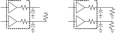
CL = 200pF to 600pF |
|
CL = 50pF to 150pF |
|
Low-speed downstream port load |
Low-speed upstream port load |
|
|
Figure 7-8. Low-speed Port Loads
Note: the CL for low-speed port load only represents the range of loading that might be added when the low-speed device is attached to a hub. The low-speed buffer must be designed to drive the load of its attached cable plus CL. A low-speed buffer design that can drive the downstream port test load would be capable of driving any legitimate upstream load.
7.1.2.1 Driver Usage
The upstream ports (towards the host) of all hubs and full-speed functions must use full-speed drivers. The upstream hub port transmits data at both fulland low-speed data rates. However, the signaling always uses full-speed signaling conventions and edge rates (refer to Figure 7-13 Upstream Full Speed Port Transceiver and Table 7-1 Signaling Levels). Transmission of low-speed data does not change the driver’s characteristics. The upstream port of low-speed functions must use a low-speed driver.
External downstream ports of all hubs (including the host), are required to be capable of both driver characteristics, such that any type of device can be plugged in to these ports. When the transceiver is in full-speed mode it uses full-speed signaling conventions and edge rates. In low-speed it uses low-speed signaling conventions and edge rates (refer to Figure 7-14 Downstream Port Transceiver and Table 7-1 Signaling Levels).
7.1.3 Cable Skew
The maximum skew introduced by the cable between the differential signaling pair (i.e., D+ and D- (TSKEW)) must be less than 400pS and is measured as described in Section 6.7.
7.1.4 Receiver Characteristics
A differential input receiver must be used to accept the USB data signal. The receiver must feature an input sensitivity (VDI) of at least 200mV when both differential data inputs are in the differential common mode range (VCM) of 0.8V to 2.5V, as shown in Figure 7-9.
In addition to the differential receiver, there must be a single-ended receiver for each of the two data lines. The receivers must have a switching threshold between 0.8V (VIL) and 2.0V (VIH). It is recommended that the single-ended receivers incorporate hysteresis to reduce their sensitivity to noise.
Both D+ and D- may temporarily be less than Vih(min) during differential signal transitions. This period can be up to 14ns (TFST) for full-speed transitions and up to 210ns (TLST) for low-speed transitions. Logic in the receiver must ensure that that this is not interpreted as an SE0.
112
Universal Serial Bus Specification Revision 1.1
Differential Input Voltage Range
Differential Output
Crossover
Voltage Range
-1.0 |
0.0 |
0.2 |
0.4 |
0.6 |
0.8 |
1.0 |
1.2 |
1.4 |
1.6 |
1.8 |
2.0 |
2.2 |
2.4 |
2.6 |
2.8 |
3.0 |
3.2 |
4.6 |
Input Voltage Range (volts)
Figure 7-9. Differential Input Sensitivity Range
7.1.5 Device Speed Identification
The USB is terminated at the hub and function ends as shown in Figure 7-10 and Figure 7-11. Full-speed and low-speed devices are differentiated by the position of the pull-up resistor on the downstream end of the cable:
Full-speed devices are terminated as shown in Figure 7-10 with the pull-up resistor on the D+ line.
Low-speed devices are terminated as shown in Figure 7-11 with the pull-up resistor on the D- line.
The pull-down terminators on downstream ports are resistors of 15k 5% connected to ground.
The design of the pull-up resistor must ensure that the signal levels satisfy the requirements specified in Table 7-1. In order to facilitate bus state evaluation that may be performed at the end of a reset, the design must be able to pull-up D+ or D- from 0V to VIH (min) within the minimum reset relaxation time of 2.5 s. A device that has a detachable cable must use a 1.5k 5% resistor tied to a voltage source between 3.0V and 3.6V (VTERM) to satisfy these requirements. Devices with captive cables may use alternative termination means. However, the Thevenin resistance of any termination must be no less than 900 .
Note: Thevenin resistance of termination does not include the 15k 5% resistor on host/hub.
The voltage source on the pull-up resistor must be derived from or controlled by the power supplied on the USB cable such that when VBUS is removed, the pull-up resistor does not supply current on the data line to which it is attached.
|
D+ |
Full-speed or |
Rpd |
Low-speed USB |
|
Transceiver |
D- |
|
Rpd |
Host or |
|
Hub Port |
|
Z 0=90 15%
Rpd=15K 5%
Rpu=1.5K 5%
Rpu |
D+ |
Full-speed USB |
Transceiver |
D- |
Hub Upstream Port |
or |
Full-speed Function |
Figure 7-10. Full-speed Device Cable and Resistor Connections
113
Universal Serial Bus Specification Revision 1.1
Full-speed or |
D+ |
|
|
Low-speed USB |
Rpd |
Transceiver |
D- |
|
|
|
Rpd |
Host or |
|
Hub Port |
|
Rpd=15K 5%
Rpu=1.5K 5% (nominal)
Rpu |
|
D+ Low-speed USB |
|
|
Transceiver |
D- |
Slow Slew Rate |
|
Buffers |
Low-speed Function |
|
Figure 7-11. Low-speed Device Cable and Resistor Connections
7.1.6 Input Characteristics
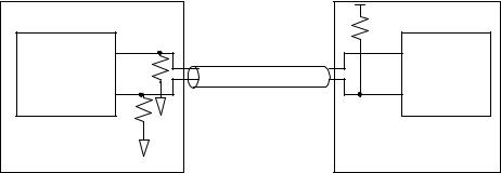
The input impedance of D+ or D- without termination should be 300 k (ZINP). The input capacitance of a port is measured at the connector pins. Upstream and downstream ports are allowed different values of capacitance. The maximum capacitance (differential or single-ended) (CIND) allowed on a downstream port of a hub or host is 150pF on D+ or D-. This is comprised of up to 75pF of lumped capacitance to ground on each line at the transceiver and in the connector, and an additional 75pF capacitance on each conductor in the transmission line between the receptacle and the transceiver. The transmission line between the receptacle and RS must be 90 15%).
The maximum capacitance on an upstream port of a full-speed device with a detachable cable (CINUB) is 100pF on D+ or D- . This is comprised of up to 75 pF of lumped capacitance to ground on each line at the transceiver and in the connector, and an additional 25pF capacitance on each conductor in the transmission line between the receptacle and the transceiver. The difference in capacitance between D+ and D- must be less than 10%.
For full-speed devices with captive cables, the device itself may have up to 75pF of lumped capacitance to ground on on D+ and D-. The cable accounts for the remainder of the input capacitance .
A low-speed device is required to have a captive cable. The input capacitance of the low-speed device will include the cable. The maximum single-ended or differential input capacitance of a low-speed device is 450pF (CLINUA).
For devices with captive cables, the single-ended input capacitance must be consistent with the termination scheme used. The termination must be able to charge the D+ or D- line from 0V to VIH (min) within 2.5 s. The capacitance on D+/D- includes the single-ended input-capacitance of the device (measured from the pins on the connector on the cable) and the 150pF of input capacitance of the host/hub.
An implementation may use small capacitors at the transceiver for purposes of edge rate control. The sum of the capacitance of the added capacitor (CEDGE) , the transceiver, and the trace connecting capacitor and transceiver to RS must not exceed 75pF (either single-ended or differential) and the capacitance must be balanced to within 10%. The added capacitor, if present, must be placed between the transceiver pins and RS (see Figure 7-12).
Use of ferrite beads on the D+ or D- lines of full-speed devices is discouraged.
114
Universal Serial Bus Specification Revision 1.1
RS
TxD+
 CEDGE
CEDGE
RS
TxD-
 CEDGE
CEDGE
Figure 7-12. Placement of Optional Edge Rate Control Capacitors
7.1.7 Signaling Levels
Table 7-1 summarizes the USB signaling levels. The source is required to drive the levels specified in the second column and the target is required to identify the correct bus state when it sees the levels in the third column. (Target receivers can be more sensitive as long as they are within limits specified in the fourth column).
115
Universal Serial Bus Specification Revision 1.1
Table 7-1. Signaling Levels
Bus State |
Signaling Levels |
|
|
|
|
|
|
|
At originating source |
At final target connector |
|
|
connector (at end of bit time) |
|
|
|
Required |
Acceptable |
|
|
|
||
|
|
|
|
Differential “1” |
D+ > VOH (min) and D- < VOL (max) |
(D+) - (D-) 200mV |
(D+) - (D-) 200mV |
|
|
and D+ VIH (min) |
|
|
|
|
|
Differential “0” |
D- > VOH (min) and D+ < VOL (max) |
(D-) - (D+) > 200mV |
(D-) - (D+) > 200mV |
|
|
and D- VIH (min) |
|
|
|
|
|
Single-ended 0 (SE0) |
D+ and D- < VOL (max) |
D+ and D- < VIL (max) |
D+ and D- < VIH (min) |
|
|
|
|
Data J state: |
|
|
|
Low-speed |
Differential “0” |
Differential “0” |
|
Full-speed |
Differential “1” |
Differential “1” |
|
|
|
|
|
Data K state: |
|
|
|
Low-speed |
Differential “1” |
Differential “1” |
|
Full-speed |
Differential “0” |
Differential “0” |
|
|
|
|
|
Idle state: |
N.A. |
|
|
Low-speed |
|
D- > VIHZ (min) and |
D- > VIHZ (min) and |
|
|
D+ < VIL (max) |
D+ < VIH (min) |
Full-speed |
|
D+ > VIHZ (min) and |
D+ > VIHZ (min) and |
|
|
|
|
|
|
D- < VIL (max) |
D- < VIH (min) |
|
|
|
|
Resume state |
Data K state |
Data K state |
|
|
|
|
|
Start-of-Packet (SOP) |
Data lines switch from Idle to K state |
|
|
|
|
|
|
End-of-Packet (EOP)4 |
SE0 for approximately 2 bit times1 |
SE0 for 1 bit time2 |
SE0 for 1 bit time2 |
|
followed by a J for 1 bit time3 |
followed by a J state |
followed by a J state |
|
|
for 1 bit time |
|
|
|
|
|
Disconnect |
N.A. |
SE0 for 2.5 s |
|
(at downstream port) |
|
|
|
|
|
|
|
Connect |
N.A. |
Idle for 2ms |
Idle for 2.5 s |
(at downstream port) |
|
|
|
|
|
|
|
Reset |
D+ and D- VOL (max) for 10ms |
D+ and D- VIL (max) |
D+ and D- VIL (max) |
|
|
for 10ms |
for 2.5 s |
|
|
|
|
Note 1: The width of EOP is defined in bit times relative to the speed of transmission. (Specification EOP widths are given in Table 7-5 and Table 7-6.)
Note 2: The width of EOP is defined in bit times relative to the device type receiving the EOP. The bit time is approximate.
Note 3: The width of the J state following the EOP is defined in bit times relative to the buffer edge rate. The J state from a low-speed buffer must be a low-speed bit time wide and from a full-speed buffer, a full-speed bit time wide.
Note 4: The keep-alive is a low-speed EOP.
116
Universal Serial Bus Specification Revision 1.1
The J and K data states are the two logical levels used to communicate differential data in the system. Differential signaling is measured from the point where the data line signals cross over. Differential data signaling is not concerned with the level at which the signals cross, as long as the crossover voltage meets the requirements in Section 7.1.2. Note that, at the receiver, the Idle and Resume states are logically equivalent to the J and K states respectively.
As shown in Table 7-1, the J and K states for full-speed signaling are inverted from those for low-speed signaling. The sense of data, idle, and resume signaling is set by the type of device that is being attached to a port. If a full-speed device is attached to a port, that segment of the USB uses full-speed signaling conventions (and fast rise and fall times), even if the data being sent across the data lines is at the lowspeed data rate. The low-speed signaling conventions shown in Table 7-1 (plus slow rise and fall times) are used only between a low-speed device and the port to which it is attached.
3.0V V 3.6V
1.5K
or equivalent
D+
 RxD
RxD
D-
Differential Receiver
 RxD+
RxD+
Single-ended Receivers
 RxD-
RxD-
 TxD+
TxD+
Output Buffers 
 OE
OE
 TxD-
TxD-
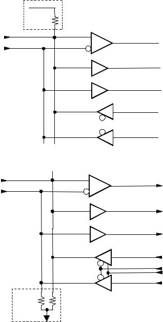
Figure 7-13. Upstream Full-speed Port Transceiver
D+
D- |
RxD |
|
|
|
Differential Receiver |
|
RxD+ |
Single-ended Receivers |
|
|
RxD- |
|
TxD+ |
Output Buffers |
OE |
|
Speed |
|
TxD- |
Note: additional logic is required |
|
15K |
to invert signal polarity on |
|
data in/out when low-speed |
|
devices are attached. |
Figure 7-14. Downstream Port Transceiver
117
Universal Serial Bus Specification Revision 1.1
7.1.7.1 Connect and Disconnect Signaling
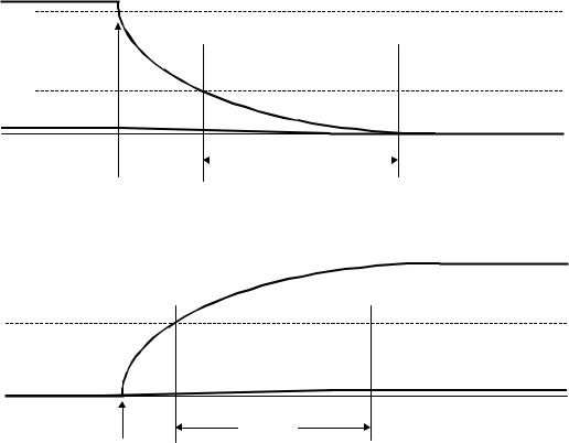
When no function is attached to the downstream port of the host or hub, the pull-down resistors present there will cause both D+ and D- to be pulled below the single-ended low threshold of the host or hub port when that port is not being driven by the hub. This creates an SE0 state on the downstream port. A disconnect condition (TDDIS) is indicated if the host or hub is not driving the data lines and an SE0 persists on a downstream port for more than 2.5 s (see Figure 7-15).
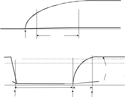
A connect condition (TDCNN) will be detected when the hub detects that one of the data lines is pulled above its VIH threshold for more than 2.5 s (see Figure 7-16 and Figure 7-17).
Hubs may optionally determine the speed of the attached device by sampling the state of the bus immediately before driving SE0 to indicate a reset condition to the device. Alternatively, the hub may float the bus after driving reset and perform bus state evaluation after 2.5 s as shown in Figure 7-18.
All signaling levels given in Table 7-1 are set for this bus segment (and this segment alone) once the speed of the attached device is determined. The mechanics of speed detection are described in Section 11.8.2.
D+/D-
VIHZ (min)


VIL


D-/D+
VSS
|
|
2.5 S |
|
|
Device |
|
Disconnect |
||
|
|
|||
|
|
|||
Disconnected |
|
|
Detected |
|
Figure 7-15. Disconnect Detection
|
D+ |
VIH |
|
VSS |
D- |
|
|
|
2.5 S |
Device |
Connect |
Connected |
Detected |
Figure 7-16. Full-speed Device Connect Detection
118
Universal Serial Bus Specification Revision 1.1
|
D- |
VIH |
|
VSS |
D+ |
|
|
|
2.5 s |
Device |
Connect |
Connected |
Detected |
Figure 7-17. Low-speed Device Connect Detection
VOH(min) 


VIH(min)
Differential
data lines
VIL 


VIL(max) 


VOL(max) 


VSS
Diff 1 or |
|
|
|
10ms |
|
2.5 s |
|
Diff 0 |
|
||
|
SE0 |
|
|
Port driving reset
Reset completed and bus is floated
Bus evaluated after reset: Diff 1 = FS connected Diff 0 = LS connected SE0 = Disconnected
Figure 7-18. Bus State Evaluation after reset (optional)
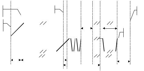
Because USB components may be hot plugged, and hubs may implement power switching, it is necessary to comprehend the delays between power switching and/or device attach and when the device’s internal power has stabilized. Figure 7-19 shows all the events associated with both turning on port power with a device connected and hot-plugging a device. There are six delays and a sequence of events that are defined by this specification.
119
Universal Serial Bus Specification Revision 1.1
Hub port |
|
|
|
|
Attach Detected |
|
|
|
|
|
|
|
|
|
|
|
|
|
|
|
|
|
|
|
|
|
|
|
|
Reset Recovery |
|||||||||||
power OK |
|
|
|
|
|
|
|
|
|
|
|
|
|
|
|
|
|
|
|
|
|
|
|
|
|
|
|
|
|
|
|
|
|
|
|
|
|
Time |
|||
Hub port |
|
|
|
|
|
|
|
|
|
|
|
|
|
|
|
|
|
|
|
|
|
|
|
|
|
|
|
|
|
|
|
|
|
|
|
|
|
|
|
||
|
|
|
|
|
|
|
|
|
|
|
|
|
|
|
|
|
|
|
|
|
|
|
|
|
|
|
|
|
|
|
|
|
|
|
|
|
|
|
|||
power-on |
|
|
|
|
|
|
|
|
|
|
|
|
|
|
|
|
|
|
|
|
|
|
|
|
|
|
|
|
|
|
|
|
|
|
|
|
|
|
|
||
|
|
|
|
|
|
|
4.01V |
|
|
|
|
|
|
|
|
|
|
t4 |
|
|
t5 |
|
|
USB System Software |
|||||||||||||||||
VBUS |
|
|
|
|
|
|
|
|
|
|
|
|
|
|
|
|
|
|
|
|
|
|
|
|
|
|
|
|
|
|
|
|
|
|
|
|
|
|
reads device speed |
||
VIH(min) |
|
|
|
|
|
|
|
|
|
|
|
|
|
|
|
|
|
|
|
|
|
|
|
|
|
|
|
|
|
|
|
|
|
|
|
|
|
|
|
||
|
|
|
|
|
|
|
|
|
|
|
|
|
|
|
|
|
|
|
|
|
|
|
|
|
|
|
|
|
|
|
|
|
|
|
|
|
|
|
|||
|
|
|
|
|
|
|
|
|
|
|
|
|
|
|
|
|
|
|
|
|
|
|
|
|
|
|
|
|
|
|
|
|
|
|
|
|
|
|
|||
VIH |
|
|
|
|
|
|
|
|
|
|
|
|
|
|
|
|
|
|
|
|
|
|
|
|
|
|
|
|
|
|
|
|
|
|
|
|
|
|
|
||
D+ |
|
|
|
|
|
|
|
|
|
|
|
|
|
|
|
|
|
|
|
|
|
|
|
|
|
|
|
|
|
|
|
|
|
|
|
|
|
|
|
|
|
or |
|
|
|
|
|
|
|
|
|
|
|
|
|
|
|
|
|
|
|
|
|
|
|
|
|
|
|
|
|
|
|
|
|
|
|
|
|
|
|
||
D- |
|
|
|
|
|
|
|
|
|
|
|
|
|
|
|
|
|
|
|
|
|
|
|
|
|
|
|
|
|
|
|
|
|
|
|
|
10ms |
|
|||
|
|
|
|
|
100ms |
|
|
|
|
|
|
|
|
|
|
|
|
|
|
|
|
|
|
|
|
|
|
|
|
|
|||||||||||
|
|
|
|
|
|
|
|
|
|
|
|
|
|
|
|
|
|
|
|
|
|
|
|
|
|
|
|
|
|
|
|
|
|
|
|
||||||
|
|
|
|
t1 |
|
t2 |
|
|
|
|
|
|
|
|
100ms |
|
|
|
|
|
|
|
|
|
|
|
t6 |
||||||||||||||
|
|
|
|
|
|
|
|
|
|
|
|
|
|
|
|
|
|
|
t3 |
|
|
|
|
|
|
|
|
|
|
|
|||||||||||
|
|
|
|
|
|
|
|
|
|
|
|
|
|
|
|
|
|
|
|
|
|
|
|
|
|
|
|
|
|
|
|
|
|||||||||
Figure 7-19. Power-on and Connection Events Timing
t1 This is the amount of time required for the hub port power switch to operate. This delay is a function of the type of hub port switch. Hubs report this time in the hub descriptor (see Section 11.15.2.1), which can be read via a request to the Hub Controller (see Section 11.16.2.4). If a device were plugged into a non-switched or already-switched on port, t1 is equal to zero.
t2 (TSIGATT)This is the maximum time from when VBUS is up to valid level (4.01V) to when a device has to signal attach. t2 represents the time required for the device’s internal power rail to stabilize and for D+ or D- to reach VIH (min) at the hub. t2 must be less than 100ms for all hub and device implementations. (This requirement only applies if the device is drawing power from the bus).
t3 (TATTDB) This is a debounce interval with a minimum duration of 100ms that is provided by the USB System Software. It ensures that the electrical and mechanical connection is stable before software attempts to reset the attached device. The interval starts when the USB System Software is notified of a connection detection. The interval restarts if there is a disconnect. The debounce interval ensures that power is stable at the device for at least 100ms before any requests will be sent to the device.
t4 (T2SUSP) Anytime a device observes no bus activity, it must obey the rules of going into suspend (see Section 7.1.7.4).
t5 (TDRST) This is the period of time hubs drive reset to a device. Refer to Section 11.5.1.5 for details.
t6 (TRSTRCY) The USB System Software guarantees a minimum of 10ms for reset recovery. Device response to any bus transactions addressed to the default device address during the reset recovery time is undefined.
120
Universal Serial Bus Specification Revision 1.1
7.1.7.2 Data Signaling
Data transmission within a packet is done with differential signals.
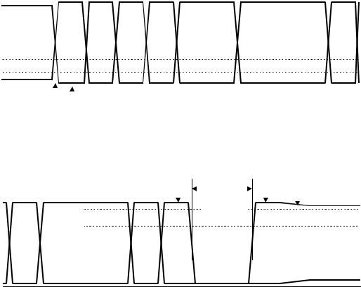
The start of a packet (SOP) is signaled by the originating port by driving the D+ and D- lines from the Idle state to the opposite logic level (K state). This switch in levels represents the first bit of the SYNC field. Hubs must limit the change in the width of the first bit of SOP when it is retransmitted to less than 5ns. Distortion can be minimized by matching the nominal data delay through the hub with the output enable delay of the hub.
The SE0 state is used to signal an end-of-packet (EOP). EOP will be signaled by driving D+ and D- to the SE0 state for two bit times followed by driving the lines to the J state for one bit time. The transition from the SE0 to the J state defines the end of the packet at the receiver. The J state is asserted for one bit time and then both the D+ and D- output drivers are placed in their high-impedance state. The bus termination resistors hold the bus in the Idle state. Figure 7-20 shows the signaling for start and end of a packet.
VOH(min)


VIH(min)


VIL(max) |
|
|
||
VOL(max) |
|
|
||
VSS |
|
|
|
|
Bus Idle |
|
|
First Bit |
|
|
|
|||
|
|
|
|
|
|
SOP |
|||
|
|
|||
|
of Packet |
|||
|
|
|
||
Last Bit |
|
Bus Driven to |
|
|||||
of Packet |
|
J State at end |
|
|||||
|
|
|
|
|
of EOP |
|
||
|
|
|
|
|
|
|||
|
|
|
SE0 |
|
|
Bus |
|
|
|
|
|
|
|
|
|||
|
|
|
|
|
Floats |
|
||
|
|
|
portion |
|
Bus Idle |
|||
|
|
|
|
|
|
|||
|
|
|
|
|
|
|||
|
|
|
of EOP |
|
|
|
||
|
|
|
|
|
|
|
||
|
|
|
|
|
|
|
||
VOH(min) 


VIH(min)


VIL(max)


VOL(max)


VSS
Figure 7-20. Packet Voltage Levels
121
Universal Serial Bus Specification Revision 1.1
7.1.7.3 Reset Signaling
A hub signals reset to a downstream port by driving an extended SE0 at the port. After the reset is removed, the device will be in the Default state (refer to Section 9.1).
The reset signaling can be generated on any Hub or Host Controller port by request from the USB System Software. The reset signaling must be driven for a minimum of 10ms (TDRST). After the reset, the hub port will transition to the Enabled state (refer to Section 11.5). Host Controllers and the USB System Software must ensure that resets issued to the root ports drive reset long enough to overwhelm any concurrent resume attempts by downstream devices. Resets from root ports should be nominally 50ms (TDRSTR). It is not required that this be 50ms of continuous Reset signaling. However, if the reset is not continuous, the interval(s) between signaling reset must be less than 3ms (TRHRSI).
A device seeing an SE0 on its upstream port for more than 2.5 s (TDETRST) may treat that signal as a reset. The reset must have taken effect before the reset signaling ends.
Hubs will propagate traffic to a newly reset port after the port is in the Enabled state. The device attached to this port must recognize this bus activity and keep from going into the Suspend state.
Hubs must be able to accept all hub requests and devices must be able to accept a SetAddress() request (refer to Section 11.16.2 and Section 9.4 respectively) after the reset recovery time 10ms (TRSTRCY) after the reset is removed. Failure to accept this request may cause the device not to be recognized by the USB system software. Hubs and devices must complete commands within the times specified in Chapter 9 and Chapter 11.
Reset must wake a device from the Suspend state.
7.1.7.4 Suspending
All devices must support the Suspend state. Devices can go into the Suspend state from any powered state. They begin the transition to the Suspend state after they see a constant Idle state on their upstream bus lines for more than 3.0ms. The device must actually be suspended, drawing only suspend current from the bus after no more than 10ms of bus inactivity on all its ports. Any bus activity on the upstream port will keep a device out of the Suspend state. In the absence of any other bus traffic, the SOF token (refer to
Section 8.4.2) will occur once per frame to keep full-speed devices from suspending. In the absence of any low-speed traffic, low-speed devices will see at least one keep-alive (defined in Table 7-1) in every frame in which an SOF occurs, which keeps them from suspending. Hubs generate this keep-alive as described in Section 11.8.4.1.
While in the Suspend state, a device must continue to provide power to its D+ (full-speed) or D- (lowspeed) pull-up resistor to maintain an idle so that the upstream hub can maintain the correct connectivity status for the device.
7.1.7.4.1 Global Suspend
Global suspend is used when no communication is desired anywhere on the bus and the entire bus is placed in the Suspend state. The host signals the start of global suspend by ceasing all its transmissions (including the SOF token). As each device on the bus recognizes that the bus is in the Idle state for the appropriate length of time, it goes into the Suspend state.
7.1.7.4.2 Selective Suspend
Segments of the bus can be selectively suspended by sending the command SetPortFeature(PORT_SUSPEND) to the hub port to which that segment is attached. The suspended port will block activity to the suspended bus segment and devices on that segment will go into the Suspend state after the appropriate delay as described above.
122