
- •Chapter 1
- •1.1 Motivation
- •1.2 Objective of the Specification
- •1.3 Scope of the Document
- •1.4 Document Organization
- •Chapter 2
- •Chapter 3
- •3.1 Goals for the Universal Serial Bus
- •3.2 Taxonomy of Application Space
- •3.3 Feature List
- •Chapter 4
- •4.1 USB System Description
- •4.1.1 Bus Topology
- •4.2 Physical Interface
- •4.2.1 Electrical
- •4.2.2 Mechanical
- •4.3 Power
- •4.3.1 Power Distribution
- •4.3.2 Power Management
- •4.4 Bus Protocol
- •4.5 Robustness
- •4.5.1 Error Detection
- •4.5.2 Error Handling
- •4.6 System Configuration
- •4.6.1 Attachment of USB Devices
- •4.6.2 Removal of USB Devices
- •4.6.3 Bus Enumeration
- •4.7 Data Flow Types
- •4.7.1 Control Transfers
- •4.7.2 Bulk Transfers
- •4.7.3 Interrupt Transfers
- •4.7.4 Isochronous Transfers
- •4.7.5 Allocating USB Bandwidth
- •4.8 USB Devices
- •4.8.1 Device Characterizations
- •4.8.2 Device Descriptions
- •4.9 USB Host: Hardware and Software
- •4.10 Architectural Extensions
- •Chapter 5
- •5.1 Implementer Viewpoints
- •5.2 Bus Topology
- •5.2.1 USB Host
- •5.2.2 USB Devices
- •5.2.3 Physical Bus Topology
- •5.2.4 Logical Bus Topology
- •5.2.5 Client Software-to-function Relationship
- •5.3 USB Communication Flow
- •5.3.1 Device Endpoints
- •5.3.2 Pipes
- •5.4 Transfer Types
- •5.5 Control Transfers
- •5.5.1 Control Transfer Data Format
- •5.5.2 Control Transfer Direction
- •5.5.3 Control Transfer Packet Size Constraints
- •5.5.4 Control Transfer Bus Access Constraints
- •5.5.5 Control Transfer Data Sequences
- •5.6 Isochronous Transfers
- •5.6.1 Isochronous Transfer Data Format
- •5.6.2 Isochronous Transfer Direction
- •5.6.3 Isochronous Transfer Packet Size Constraints
- •5.6.4 Isochronous Transfer Bus Access Constraints
- •5.6.5 Isochronous Transfer Data Sequences
- •5.7 Interrupt Transfers
- •5.7.1 Interrupt Transfer Data Format
- •5.7.2 Interrupt Transfer Direction
- •5.7.3 Interrupt Transfer Packet Size Constraints
- •5.7.4 Interrupt Transfer Bus Access Constraints
- •5.7.5 Interrupt Transfer Data Sequences
- •5.8 Bulk Transfers
- •5.8.1 Bulk Transfer Data Format
- •5.8.2 Bulk Transfer Direction
- •5.8.3 Bulk Transfer Packet Size Constraints
- •5.8.4 Bulk Transfer Bus Access Constraints
- •5.8.5 Bulk Transfer Data Sequences
- •5.9 Bus Access for Transfers
- •5.9.1 Transfer Management
- •5.9.2 Transaction Tracking
- •5.9.3 Calculating Bus Transaction Times
- •5.9.4 Calculating Buffer Sizes in Functions and Software
- •5.9.5 Bus Bandwidth Reclamation
- •5.10 Special Considerations for Isochronous Transfers
- •5.10.1 Example Non-USB Isochronous Application
- •5.10.2 USB Clock Model
- •5.10.3 Clock Synchronization
- •5.10.4 Isochronous Devices
- •5.10.5 Data Prebuffering
- •5.10.6 SOF Tracking
- •5.10.7 Error Handling
- •5.10.8 Buffering for Rate Matching
- •Chapter 6
- •6.1 Architectural Overview
- •6.3 Cable
- •6.4 Cable Assembly
- •6.4.1 Detachable Cable Assemblies
- •6.4.3 Low-speed Captive Cable Assemblies
- •6.4.4 Prohibited Cable Assemblies
- •6.5.1 USB Icon Location
- •6.5.2 USB Connector Termination Data
- •6.5.3 Series “A” and Series “B” Receptacles
- •6.5.4 Series “A” and Series “B” Plugs
- •6.6.1 Description
- •6.6.2 Construction
- •6.6.3 Electrical Characteristics
- •6.6.4 Cable Environmental Characteristics
- •6.6.5 Listing
- •6.7 Electrical, Mechanical and Environmental Compliance Standards
- •6.7.1 Applicable Documents
- •6.8 USB Grounding
- •Chapter 7
- •7.1 Signaling
- •7.1.1 USB Driver Characteristics
- •7.1.2 Data Signal Rise and Fall
- •7.1.3 Cable Skew
- •7.1.4 Receiver Characteristics
- •7.1.5 Device Speed Identification
- •7.1.6 Input Characteristics
- •7.1.7 Signaling Levels
- •7.1.8 Data Encoding/Decoding
- •7.1.9 Bit Stuffing
- •7.1.10 Sync Pattern
- •7.1.11 Data Signaling Rate
- •7.1.12 Frame Interval and Frame Interval Adjustment
- •7.1.13 Data Source Signaling
- •7.1.14 Hub Signaling Timings
- •7.1.15 Receiver Data Jitter
- •7.1.16 Cable Delay
- •7.1.17 Cable Attenuation
- •7.1.18 Bus Turn-around Time and Inter-packet Delay
- •7.1.19 Maximum End-to-end Signal Delay
- •7.2 Power Distribution
- •7.2.1 Classes of Devices
- •7.2.2 Voltage Drop Budget
- •7.2.3 Power Control During Suspend/Resume
- •7.2.4 Dynamic Attach and Detach
- •7.3 Physical Layer
- •7.3.1 Regulatory Requirements
- •7.3.2 Bus Timing/Electrical Characteristics
- •7.3.3 Timing Waveforms
- •Chapter 8
- •8.1 Bit Ordering
- •8.2 SYNC Field
- •8.3 Packet Field Formats
- •8.3.1 Packet Identifier Field
- •8.3.2 Address Fields
- •8.3.3 Frame Number Field
- •8.3.4 Data Field
- •8.3.5 Cyclic Redundancy Checks
- •8.4 Packet Formats
- •8.4.1 Token Packets
- •8.4.2 Start-of-Frame Packets
- •8.4.3 Data Packets
- •8.4.4 Handshake Packets
- •8.4.5 Handshake Responses
- •8.5 Transaction Formats
- •8.5.1 Bulk Transactions
- •8.5.2 Control Transfers
- •8.5.3 Interrupt Transactions
- •8.5.4 Isochronous Transactions
- •8.6 Data Toggle Synchronization and Retry
- •8.6.1 Initialization via SETUP Token
- •8.6.2 Successful Data Transactions
- •8.6.3 Data Corrupted or Not Accepted
- •8.6.4 Corrupted ACK Handshake
- •8.6.5 Low-speed Transactions
- •8.7 Error Detection and Recovery
- •8.7.1 Packet Error Categories
- •8.7.2 Bus Turn-around Timing
- •8.7.3 False EOPs
- •8.7.4 Babble and Loss of Activity Recovery
- •Chapter 9
- •9.1 USB Device States
- •9.1.1 Visible Device States
- •9.1.2 Bus Enumeration
- •9.2 Generic USB Device Operations
- •9.2.1 Dynamic Attachment and Removal
- •9.2.2 Address Assignment
- •9.2.3 Configuration
- •9.2.4 Data Transfer
- •9.2.5 Power Management
- •9.2.6 Request Processing
- •9.2.7 Request Error
- •9.3 USB Device Requests
- •9.3.1 bmRequestType
- •9.3.2 bRequest
- •9.3.3 wValue
- •9.3.4 wIndex
- •9.3.5 wLength
- •9.4 Standard Device Requests
- •9.4.1 Clear Feature
- •9.4.2 Get Configuration
- •9.4.3 Get Descriptor
- •9.4.4 Get Interface
- •9.4.5 Get Status
- •9.4.6 Set Address
- •9.4.7 Set Configuration
- •9.4.8 Set Descriptor
- •9.4.9 Set Feature
- •9.4.10 Set Interface
- •9.4.11 Synch Frame
- •9.5 Descriptors
- •9.6 Standard USB Descriptor Definitions
- •9.6.1 Device
- •9.6.2 Configuration
- •9.6.3 Interface
- •9.6.4 Endpoint
- •9.6.5 String
- •9.7 Device Class Definitions
- •9.7.1 Descriptors
- •9.7.2 Interface(s) and Endpoint Usage
- •9.7.3 Requests
- •Chapter 10
- •10.1 Overview of the USB Host
- •10.1.1 Overview
- •10.1.2 Control Mechanisms
- •10.1.3 Data Flow
- •10.1.4 Collecting Status and Activity Statistics
- •10.1.5 Electrical Interface Considerations
- •10.2 Host Controller Requirements
- •10.2.1 State Handling
- •10.2.2 Serializer/Deserializer
- •10.2.3 Frame Generation
- •10.2.4 Data Processing
- •10.2.5 Protocol Engine
- •10.2.6 Transmission Error Handling
- •10.2.7 Remote Wakeup
- •10.2.8 Root Hub
- •10.2.9 Host System Interface
- •10.3 Overview of Software Mechanisms
- •10.3.1 Device Configuration
- •10.3.2 Resource Management
- •10.3.3 Data Transfers
- •10.3.4 Common Data Definitions
- •10.4 Host Controller Driver
- •10.5 Universal Serial Bus Driver
- •10.5.1 USBD Overview
- •10.5.2 USBD Command Mechanism Requirements
- •10.5.3 USBD Pipe Mechanisms
- •10.5.4 Managing the USB via the USBD Mechanisms
- •10.5.5 Passing USB Preboot Control to the Operating System
- •10.6 Operating System Environment Guides
- •Chapter 11
- •11.1 Overview
- •11.1.1 Hub Architecture
- •11.1.2 Hub Connectivity
- •11.2 Hub Frame Timer
- •11.2.1 Frame Timer Synchronization
- •11.2.2 EOF1 and EOF2 Timing Points
- •11.3 Host Behavior at End-of-Frame
- •11.3.1 Latest Host Packet
- •11.3.2 Packet Nullification
- •11.3.3 Transaction Completion Prediction
- •11.4 Internal Port
- •11.4.1 Inactive
- •11.4.2 Suspend Delay
- •11.4.3 Full Suspend (Fsus)
- •11.4.4 Generate Resume (GResume)
- •11.5 Downstream Ports
- •11.5.1 Downstream Port State Descriptions
- •11.6 Upstream Port
- •11.6.1 Receiver
- •11.6.2 Transmitter
- •11.7 Hub Repeater
- •11.7.1 Wait for Start of Packet from Upstream Port (WFSOPFU)
- •11.7.2 Wait for End of Packet from Upstream Port (WFEOPFU)
- •11.7.3 Wait for Start of Packet (WFSOP)
- •11.7.4 Wait for End of Packet (WFEOP)
- •11.8 Bus State Evaluation
- •11.8.1 Port Error
- •11.8.2 Speed Detection
- •11.8.3 Collision
- •11.9 Suspend and Resume
- •11.10 Hub Reset Behavior
- •11.10.1 Hub Receiving Reset on Upstream Port
- •11.11 Hub Port Power Control
- •11.11.1 Multiple Gangs
- •11.12 Hub I/O Buffer Requirements
- •11.12.1 Pull-up and Pull-down Resistors
- •11.12.2 Edge Rate Control
- •11.13 Hub Controller
- •11.13.1 Endpoint Organization
- •11.13.2 Hub Information Architecture and Operation
- •11.13.3 Port Change Information Processing
- •11.13.4 Hub and Port Status Change Bitmap
- •11.13.5 Over-current Reporting and Recovery
- •11.14 Hub Configuration
- •11.15 Descriptors
- •11.15.1 Standard Descriptors
- •11.15.2 Class-specific Descriptors
- •11.16 Requests
- •11.16.1 Standard Requests
- •11.16.2 Class-specific Requests
- •Index
Какую работу нужно написать?

Universal Serial Bus Specification Revision 1.1
6.6 Cable Mechanical Con figuration and Material Requirements
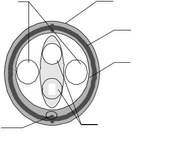
Full-speed and Low-speed cables differ in data conductor arrangement and shielding. Low-speed cable does not require twisted data conductors or a shield. Figure 6-11 shows the typical Full-speed cable construction.
Non-Twisted Power Pair: |
Polyvinyl Chloride (PVC) Jacket |
|
Red: |
VBUS |
|
Black: |
Power Ground |
|
|
|
|
Outer Shield > 65% Interwoven
Tinned Copper Braid
W
R B
G
28 AWG Tinned
Copper Drain Wire
Inner Shield Aluminum
Metallized Polyester
Twisted Signaling Pair:
White: D-
Green: D+
Figure 6-11. Typical Full-speed Cable Construction
6.6.1 Description
Full-speed cable consists of one 28 to 20 AWG non-twisted power pair and one 28 AWG twisted data pair with an aluminum metallized polyester inner shield, 28 AWG stranded tinned copper drain wire, > 65% tinned copper wire interwoven (braided) outer shield and PVC outer jacket.
Low-speed cable does not require the data pair be twisted or a shield and drain wire.
90
Universal Serial Bus Specification Revision 1.1
6.6.2Construction
Raw materials used in the fabrication of this cable shall be of such quality that the fabricated cable is capable of meeting or exceeding the mechanical and electrical performance criteria of the most current USB Specification Revision, and all applicable domestic and international safety/testing agency requirements, e.g., UL, CSA, BSA, NEC, et cetera, for electronic signaling and power distribution cables in its category.
Table 6-2. Power Pair
American Wire |
Nominal Conductor |
Stranded Tinned |
|
Gauge (AWG) |
Outer Diameter |
Conductors |
|
|
|
|
|
28 |
0.381 mm (0.015”) |
7 x 36 |
|
0.406 mm (0.016”) |
19 x 40 |
||
|
|||
|
|
|
|
26 |
0.483 mm (0.019”) |
7 x 34 |
|
0.508 mm (0.020”) |
19 x 38 |
||
|
|||
|
|
|
|
24 |
0.610 mm (0.024”) |
7 x 32 |
|
0.610 mm (0.024”) |
19 x 36 |
||
|
|||
|
|
|
|
22 |
0.762 mm (0.030”) |
7 x 30 |
|
0.787 mm (0.031”) |
19 x 34 |
||
|
|||
|
|
|
|
20 |
0.890 mm (0.035”) |
7 x 28 |
|
0.931 mm (0.037”) |
19 x 32 |
||
|
|||
|
|
|
Note: Minimum conductor construction shall be stranded tinned copper.
Non-Twisted Power Pair:
A.Wire Gauge: Minimum 28 AWG or as specified by the user contingent upon the specified cable length. Refer to Table 6-2.
B.Wire Insulation: Semirigid polyvinyl chloride (PVC).
1.Nominal Insulation Wall Thickness: 0.25 mm (0.010”).
2.Typical Power (VBUS) Conductor: Red Insulation.
3.Typical Ground Conductor: Black Insulation.
Signal Pair:
A. Wire Gauge: 28 AWG minimum. Refer to Table 6-3.
Table 6-3. Signal Pair
American Wire |
Nominal Conductor |
Stranded Tinned |
|
Gauge (AWG) |
Outer Diameter |
Conductors |
|
|
|
|
|
28 |
0.381 mm (0.015”) |
7 x 36 |
|
0.406 mm (0.016”) |
19 x 40 |
||
|
|||
|
|
|
91
Universal Serial Bus Specification Revision 1.1
Note: Minimum conductor construction shall be stranded tinned copper
B.Wire Insulation: High-density polyethylene (HDPE), alternately foamed polyethylene or foamed polypropylene.
1.Nominal Insulation Wall Thickness: 0.31 mm (0.012”).
2.Typical Data Plus (+) Conductor: Green Insulation.
3.Typical Data Minus (-) Conductor: White Insulation.
C.Nominal Twist Ratio (not required for Low-speed): One full twist every 60 mm (2.36”) to 80 mm (3.15”).
Aluminum Metallized Polyester Inner Shield (not required for Low-speed):
A.Substrate Material: Polyethylene terephthalate (PET) or equivalent material.
B.Metallizing: Vacuum deposited aluminum.
C.Assembly:
1.The aluminum metallized side of the inner shield shall be positioned facing out to ensure direct contact with the drain wire.
2.The aluminum metallized inner shield shall over lap by approximately one-quarter turn.
Drain Wire (not required for Low-speed):
A.Wire Gauge: Minimum 28 AWG stranded tinned copper (STC) non-insulated. Refer to Table 6-4.
Table 6-4. Drain Wire Signal Pair
American Wire |
Nominal Conductor |
Stranded Tinned |
|
Gauge (AWG) |
Outer Diameter |
Conductors |
|
|
|
|
|
28 |
0.381 mm (0.015”) |
7 x 36 |
|
0.406 mm (0.016”) |
19 x 40 |
||
|
|||
|
|
|
Interwoven (Braided) Tinned Copper Wire (ITCW) Outer Shield (not required for Low-speed):
A.Coverage Area: Minimum 65%.
B.Assembly. The interwoven (braided) tinned copper wire outer shield shall encase the aluminum metallized PET shielded power and signal pairs and shall be in direct contact with the drain wire.
Outer Polyvinyl Chloride (PVC) Jacket:
A.Assembly: The outer PVC jacket shall encase the fully shielded power and signal pairs and shall be in direct contact with the tinned copper outer shield.
B.Nominal Wall Thickness: 0.64 mm (0.025”).
Marking: The cable shall be legibly marked using contrasting color permanent ink.
A.Minimum marking information for Full-speed cable shall include:
USB SHIELDED <Gauge/2C + Gauge/2C> UL CM 75o C — UL Vendor ID
B.Minimum marking information for Low-speed cable shall include: USB specific marking is not required for Low-speed cable.
92
Universal Serial Bus Specification Revision 1.1
Nominal Fabricated Cable Outer Diameter:
This is a nominal value and may vary slightly from manufacturer to manufacturer as function of the conductor insulating materials and conductor specified. Refer to Table 6-5.
Table 6-5. Nominal Cable Diameter
Shielded USB |
Nominal Outer |
Cable Configuration |
Cable Diameter |
|
|
28/28 |
4.06 mm (0.160”) |
|
|
28/26 |
4.32 mm (0.170”) |
|
|
28/24 |
4.57 mm (0.180”) |
|
|
28/22 |
4.83 mm (0.190”) |
|
|
28/20 |
5.21 mm (0.205”) |
|
|
6.6.3Electrical Characteristics
All electrical characteristics shall be measured at or referenced to +20o C (68o F).
Voltage Rating: 30 Vrms maximum.
Conductor Resistance: Conductor resistance shall be measured in accordance with ASTM-D-4566 Section 13. Refer to Table 6-6.
Conductor Resistance Unbalance (Pairs): Conductor resistance unbalance between two (2) conductors of any pair shall not exceed five percent (5%) when measured in accordance with ASTM-D-4566 Section 15.
Table 6-6. Conductor Resistance
American |
Ohms ( ) / 100 Meters |
|
Wire Gauge (AWG) |
Maximum |
|
|
|
|
28 |
23.20 |
|
|
|
|
26 |
14.60 |
|
|
|
|
24 |
9.09 |
|
|
|
|
22 |
5.74 |
|
|
|
|
20 |
3.58 |
|
|
|
|
6.6.4Cable Environmental Characteristics
Temperature Range:
A.Operating Temperature Range: 0o C to +50o C.
B.Storage Temperature Range: -20o C to +60o C.
C.Nominal Temperature Rating: +20o C.
Flammability: All plastic materials used in the fabrication of this product shall meet or exceed the requirements of NEC Article 800 for communications cables Type CM (Commercial).
93