

By Frédéric Rivoallon, Xilinx, Inc.
Introduction:
Most FPGA designs today rely on an HDL based description of their design. HDL synthesis is probably the single most important software flow step when it comes to defining the performance of a design. Synthesis links the conceptual description of the logic functions needed for the design to their actual physical architecture elements in the underlying device. This step cannot be underestimated. Synthesis is performed prior to chip placement as an entirely separate step, hence these technology dependent optimizations are computed without knowledge of actual chip placement. As a result, design performance can be far from optimal, impacted by choices made too early. This is where physical synthesis comes into play, bringing physical information to the synthesis engine.
Traditional Flow versus Physical Synthesis Flow:
The most common design flows use synthesis and place & route as two consecutive disjointed steps. Synthesis generates an EDIF netlist that is then passed on to the backend for implementation. The netlist contains basic elements such as LUTs, flip-flops, etc., but does not control how these elements will be packaged together in the FPGA clusters (referred to as “slices” in Xilinx® FPGAs) during the packing phase. Synthesis also has no control on placement and often does not have access to the entire design, if cores are used as black boxes.
With physical synthesis, it’s different. Physical synthesis yields a better result because it provides information about the actual critical paths, the ones that placement is actually seeing. This is a key feature as it closes the loop between synthesis and place & route.
Figure 1 compares the two flows. The traditional flow is shown on the left and the physical synthesis flow using Xilinx® ISE™ 9.1i is shown on the right. All options in blue are explained in detail in the next section.
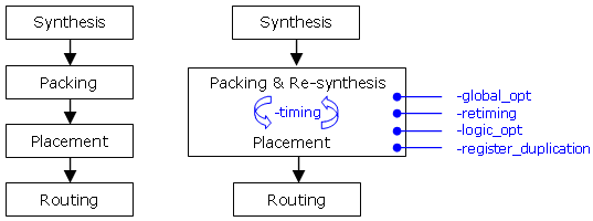
Fig 1: Traditional flow and ISE 9.1i physical synthesis flow
Another key advantage of physical synthesis is that it guarantees a better level of consistency for both the synthesis and implementation constraints. By having an integrated environment for synthesis, packing and placement, it guarantees that synthesis and place & route are working on the same problem.
An important silicon architecture consideration: The trend in modern FPGA silicon architecture is to offer more and more capable clusters (or slices). This permits more possibilities for physical synthesis flows since the traditional ISE software flow places already pre-packed slices. In effect, the traditional flow does not place LUTs and flip-flops, it actually places slices. The –timing option in ISE software enables placement at the most basic element level (non only LUTs and flip-flops but also logic fragments in the slice like dedicated arithmetic and multiplexer circuitry).
To respond to the challenge of physically aware synthesis, several approaches exist today with tools that enable synthesis optimizations aware of placement and capable of modifying technology mapping, altering clustering (packing) and enhancing placement, using information from the initial placement.
The following paragraphs provide an overview of solutions provided by Xilinx ISE 9.1i software and Synplicity® Synplify® Premier.
Physical Synthesis Optimizations in ISE Software:
ISE 9.1i software provides several physical synthesis options to improve results beyond the default compiles. These optimizations are applied on the same base netlist used in the traditional, non-physical flow. This enables ISE software to use any incoming netlist without having to rely on a particular synthesis tool. Users can also use Xilinx synthesis tool (XST) as a design entry tool for this flow.
All options are part of the MAP step of the ISE implementation flow. To enable the flow, the following options are used:
|
MAP command line option |
Description |
|
-global_opt on|off |
Optimization routines that operate on the fully assembled netlist after initial packing. These optimizations include logic remapping and trimming, logic and register replication. This option can optimize black-boxed portions of the design. |
|
-logic_opt on|off |
Post-placement logic restructuring. Operates on a placed netlist to optimize timing critical connections through restructuring and re-synthesis, followed by incremental placement and incremental timing analysis. Option is enabled in conjunction with “–timing.” |
|
-register_duplication on|off |
The option is only available when running timing-driven packing and placement with the –timing option. The option duplicates registers to improve timing when running timing-driven packing (“–timing”). |
|
-retiming on|off |
When this option is on, registers are moved through the logic to balance out the delays in a timing path to increase the overall clock frequency. By default, this option is off. It requires global_opt “on” to operate. |
|
-timing (Note: this option is always active for Virtex-5 FPGAs) |
Enables packing and placement interaction based on timing goals. When activated, placement is done during the MAP phase, therefore the –ol option should be used along with it. |
Table 1: MAP Physical Synthesis properties description.

Figure 2: MAP properties for Physical Synthesis
Alternatively, all these options (shown in red in the picture on the right) are accessible from Project Navigator, the main ISE GUI via the “Process Properties” window. Property display level must be set to “Advanced.”
The effectiveness of the options discussed above depends on a number of factors. These MAP options will have more opportunities to make improvements in the following situations:
-
Under-constraining in synthesis prevents it from generating the best optimizations. To avoid this situation, it is recommended to tightly constrain synthesis until the tool reports negative slack.
-
Inconsistent constraining between synthesis and implementation is a fairly common situation in which synthesis is not driven to optimize paths that are later constrained during implementation. Physical synthesis can likely re-build the fast logic needed to meet timing. To remedy this situation in the traditional flow, carefully examine constraints between synthesis and implementation and make sure similar paths are covered in both.
-
In a bottom-up or partition flow, synthesis may not optimize between blocks or partitions.
-
Design reuse netlist used as “black-boxes” in synthesis may limit the amount of possible optimization. Note that synthesis has the capability in the traditional flow to “read” netlists from black-boxes. This helps the tools analyze paths going to and coming from the black boxes. But sometimes these black boxes are not added to the synthesis project and this is where physical synthesis options can have a great impact.
-
Designs with high LUT to flip-flop ratio (few registers for a lot of logic) are more likely to benefit from the retiming option. Note that retiming (called register balancing in XST) is also available in synthesis and can be used as part of the traditional flow.
Even if care is taken during the synthesis step and constraints are consistent between synthesis and implementation, physical synthesis can improve performance. Following are some of the optimizations used in the algorithms:
-
Logic Duplication: If a LUT or flip-flop drives multiple loads, and the placement of one or more of those loads is too far away from the source to meet timing requirements, the LUT or flip-flop can be replicated and placed close to that group of loads, thus reducing routing delays.
-
Logic Recombination: If the critical path traverses through multiple LUTs and through multiple slices, the logic can be reassembled utilizing fewer slices by using a more timing efficient combination of LUTs and MUXes to reduce the routing resources needed for that path.
-
Basic Element Switching: If a function is built with LUTs and MUXes within a slice, physical synthesis and optimization can rearrange the function to give the fastest path (usually through the MUX select pin) to the most critical signal as shown in Figure 3:
|
|
|
|
“sig” is timing critical, it crosses a LUT and a MUX… |
“sig” is timing critical, it crosses a LUT and a MUX… |


Figure 3: Basic Element Switching Example
-
Pin Swapping: Each input pin of a LUT may have a different delay. MAP has the ability to swap pins (and change the LUT equation accordingly) so that the most critical signal is assigned to the fastest pin. This is particularly effective with the Xilinx® Virtex™-5 FPGAs since its 6-input LUTs have distributed delays, with pins 1 through 6 being increasingly faster (pin 6 being the fastest). This pin swapping capability in MAP helps predict timing with more accuracy. It should be noted that during routing, pins can also be swapped. In the traditional flow only the routing phase will operate pin swapping.
In conclusion, Xilinx ISE 9.1i software provides several options to enable physical optimizations in a one pass flow. Choosing the right one (or the right ones) can prove to be difficult. To make it easier, Xilinx provides the Xplorer utility to run the design with these optimizations and to select the best one. The Xplorer utility is available at the command line and also from the GUI with Project Navigator.
Physical Synthesis with Synplify Premier:
Synplicity offers a physical synthesis tool known as Synplify Premier. The Synplify Premier product is a graph-based physical synthesis tool that enables single-pass physical synthesis. The essence of the graph-based approach is that pre-existing wires, switches and placement sites used for routing an FPGA are represented as a detailed routing resource graph. The notion of what is a “good routing choice” then changes from delay estimation only to a measure of actual delay and availability of interconnect wires.
Synplify Premier merges optimization, packing, placement and routing to ensure available, fast routes along critical paths and generates a fully placed and physically optimized netlist as output ready for final routing in ISE software. The main benefits of this approach are the output from synthesis is routable and timing is known after synthesis because it correlates with the timing that the user will see after ISE routes the design. This approach reduces the number of synthesis runs (ISE backend iterations) involved in meeting timing goals.
Synplify Premier provides an encapsulated flow which enables the completion of a physical synthesis design without leaving the Synplify Premier graphical interface. After entering all the design files including black boxes and carefully setting up the constraints, Synplify Premier performs the steps necessary to deliver a physically optimized design:
-
The tool performs an initial synthesis (or compile) and runs the ISE software flow through placement to initialize its optimizations. See figure 4 below.
-
Synplify Premier will then read back the results to evaluate critical paths with much better accuracy compared to the traditional synthesis flow.
-
Based on this first placement, Synplify Premier keeps the I/O placement and performs a global full-chip placement.
-
Synplify Premier also performs detailed placement taking into account very specific routing characteristics and resources of the target FPGA. As explained earlier, Synplify Premier integrates the fact that proximity alone in placement does not always lead to optimal performance because routing timing delays are not always dependant on distance alone. To account for the timing differences for the various routing structures, Synplify Premier uses the graph of pre-existing wire availability when doing placement.
-
At the end of the process, Synplify Premier generates a netlist, a legal, routable placement plus a constraint file (.ncf) and then spawns the Xilinx Xflow command to finalize the design routing. Xflow will check the packing, placement and will route the circuit based on the forwarded constraint file.

Figure 4: Synplify Premier Flow
Conclusion:
Physical synthesis enables better results by bridging synthesis and place & route. Xilinx provides the technology as part of ISE 9.1i using re-synthesis algorithms that can be applied to any incoming netlists.
Synplify Premier from Synplicity provides a different implementation of this technology using its own full chip placement. An initial placement will considerably improve timing predictions due to highly accurate correlation between what Synplify Premier uses and the final post-route timing results. It ultimately provides a routing-aware placement to the ISE software that meets timing after ISE software routes the design.
The Synplify Premier solution is the industry’s ultimate FPGA implementation and debug environment. It provides a comprehensive suite of tools and technologies for advanced FPGA designers as well as ASIC prototypers targeting single FPGA-based prototypes. The Synplify Premier software is a technology independent solution that addresses the most challenging aspects of FPGA design including timing closure, logic verification, IP usage, ASIC compatibility, DSP implementation, debug, and tight integration with FPGA vendor back-end tools.

Synplify Premier: The Ultimate FPGA Implementation and Debug Environment The Synplify Premier product offers FPGA Designers and ASIC Prototypers, targeting single FPGA-based prototypes, with the most efficient method of design implementation and debug. The Synplify Premier software provides in-system verification of FPGAs, dramatically accelerates the debug process, and provides a rapid and incremental method for finding elusive design problems. The Synplify Premier software advantages include:
-
technology and vendor independence
-
in-system debug
-
fast timing closure
-
RTL analysis
-
DSP-friendly synthesis algorithms
-
superior Quality of Results (QoR)

Reach Timing Goals Quickly with Graph-based Physical Synthesis Today’s high-density FPGAs make it increasingly difficult for designers to meet their aggressive timing goals quickly. Synopsys' Synplify Premier product addresses the timing closure challenge with its patented Graph-based physical synthesis technology .
Graph-based Physical Synthesis offers:
-
patented technology
-
improved timing closure through estimations that are tightly correlated with final post place & route timing
-
90% of designs are within 10% of actual timing
-
-
assurance that correct critical paths are being optimized
-
significant reduction in design iterations and development time

Graph-based physical synthesis provides tight correlation to final timing
Find Bugs Quickly The Synplify Premier software provides a rapid method of finding functional errors in FPGA designs by providing simulator-like visibility into live-running hardware. The methodology is based on technology found in the Identify® RTL Debugger - the first and only tool that allows designers to instrument and debug directly in RTL source code. Synplify Premier’s debugger technology provides designers with:
-
ability to add probes and trigger conditions in familiar RTL source code
-
ability to see sequence of captured results annotated in context to the RTL code
-
fast, incremental debug flow ability to bypass time-consuming iterations through place & route
DSP Friendly Synthesis As DSP functionality within FPGAs continues to rise, the Synplify Premier software’s DSP-aware mapping technology takes full advantage of the dedicated DSP structures and memories built in to today’s modern FPGAs. The Synplify Premier tool’s DSP aware synthesis provides:
-
DSP-friendly synthesis algorithms
-
RTL DSP functions automatically mapped into vendors’ DSP hardware
-
tight integration with Synopsys' Synplify DSP software
ASIC Verification using Single FPGA-based Prototypes As a part of Synopsys' Confirma ASIC/ASSP Verification Platform, the Synplify Premier solution offers the most comprehensive system for implementing single FPGA-based ASIC prototypes. Synplify Premier’s ASIC prototyping features offer:
-
built-in gated clock conversion
-
Synopsys DesignWare® Support
-
tight integration with Synopsys' HAPS™ High-performance ASIC Prototyping System
|
|
HAPS-A31 prototyping board |
|
|
HAPS-51 Prototyping board |

System-Level Implementation and IP Integration The System Designer™ capability, a key component of the ReadyIP program, allows users to select, configure and assemble internal and third-party IP delivered in the IP-XACT format, integrate that IP and then easily implement it into a variety of FPGA vendor devices. The System Designer capability offers:
-
the use of Spirit IP-XACT Compliant IP
-
the ability to Configure And Interconnect IP For System
-
easy Drag & Drop Connectivity
-
easy Reuse Of In-house, Proprietary IP
-
Eclipse-based format
Access To Third Party IP for Evaluation and Download The ReadyIP Initiative is a program that simplifies the access, evaluation, and use of IP for FPGA-based system design. It is an encrypted design methodology for FPGA implementation that allows users to incorporate and easily integrate IP from several third-party vendors within their designs using Synopsys’ industry-standard synthesis environments, the Synplify Pro® and/or Synplify® Premier solutions. The ReadyIP initiative offers:
-
standards-based, accessible and secure IP distribution environment
-
easy-to-Use IP evaluation mechanism
-
IP configuration and assembly integrated into Synopsys' synthesis products
-
partnership with leading IP vendors
Digital Clock Managers (DCMs) provide advanced clocking capabilities to Spartan™-3 FPGA
applications. DCMs optionally multiply or divide the incoming clock frequency to synthesize a
new clock frequency. DCMs also eliminate clock skew, thereby improving system performance.
Similarly, a DCM optionally phase shifts the clock output to delay the incoming clock by a
fraction of the clock period. The DCMs integrate directly with the FPGA’s global low-skew clock distribution network.
Блок управления тактовыми генераторами (Digital Clock Managers (DCMs) обеспечивает расширенные возможности тактовой синхронизации для ПЛИС серии Spartan™-3. Этот блок осуществляет умножение или деление частоты от внешнего тактового генератора для получения требуемой тактовой частоты.
Он также исключает появление фазового сдвига тактовых (синхронизирующих импульсов), улучшая таким образом характеристики ПЛИС.
Эти блоки интегрируются с глобальной сетью распределения тактовых генераторов с малым значением фазового сдвига тактовых (синхронизирующих импульсов).
The Spartan-3 family architecture consists of five fundamental programmable functional elements (архитектура семейства Spartan-3 ИС состоит из 5 фундаментальных программируемых функциональных элементов):
This application note describes a technique for configuring an FPGA from an embedded
processor. Three common components are required: an embedded microprocessor, some
non-volatile memory, and a CPLD. Cost, as well as real estate, can be reduced if the function
of a dedicated configuration device, such as a PROM, can be integrated within these three
components. A system diagram is shown in Figure 1.
Note: Some systems might not require a CPLD if the microprocessor has a sufficient number of
general-purpose I/O (GPIO) pins available. For these systems, the Xilinx FPGA can be configured directly by the microprocessor. For this type of configuration, this application note still applies. The overall configuration flow remains the same, but the user must modify the source code so that the microprocessor strobes its GPIO pins instead of its address and data bus.
Instead of using a dedicated PROM, the configuration bit-stream can be loaded into unused
portions of non-volatile system memory. Furthermore, a microprocessor, whose primary
purpose is to perform other tasks, can also be used to coordinate the loading of configuration
data into a Xilinx FPGA device. Unused register bits of a CPLD accessible to the
microprocessor can then be used to monitor and instrument the FPGA’s control, data, and
status bits. Microprocessors typically have a limited number of control signals, and a simple
CPLD design can map a portion of the microprocessor’s address space to control FPGA
configuration. Using this method, the CPLD establishes a synchronous interface between the
microprocessor and the Xilinx FPGA. Such an interface can also allow the microprocessor to
do more advanced functions, such as partial reconfiguration and read-back.
CPLD ( Complex Programmable Logic Device) сложное устройство с программируемой логикой технология, разработанная фирмой Xilinx

Motorola DragonBall EZ Microprocessor
Motorola/Freescale Semiconductor's DragonBall, or MC68328, is a microcontroller design based on the famous 68000 core, but implemented as an all-in-one low-power solution for handheld computeruse. It was designed by Motorola in Hong Kong.
The processor is capable of speeds of up to 16.58 MHz and can run up to 2.7 MIPS (million instructions per second), for the base 68328 and DragonBall EZ (MC68EZ328) model. It was extended to 33 MHz, 5.4 MIPS for the DragonBall VZ (MC68VZ328) model, and 66 MHz, 10.8 MIPS for the DragonBall Super VZ(MC68SZ328).
It is a 32-bit processor with 32-bit internal and external address bus (24-bit external address bus for EZ and VZ variants). It has many built-in functions, like a color and grayscale display controller, PC speaker sound, serial port with UART and IRDA support, UART bootstrap, real time clock, is able to directly access DRAM, Flash ROM, and mask ROM, and has built-in support for touch screens.
It is an all-in-one computer on a chip; before the DragonBall EZ, Palm handhelds had twice as many ICs.

