

Implement Design and Verify Constraints (реализация разработки и верификация ограничений).
Implement the design and verify that it meets the timing constraints specified in the previous section.
Implementing the Design (реализация разработки).
1. Select the counter source file in the Sources window (выберите файл counter source (документ счетчика) в окне Sources (документы);
2. Open the Design Summary by double-clicking the View Design Summary process in the Processes tab (откройте окно Design Summary (итоги разработки) двойным щелчком по пиктограмме View Design Summary (просмотр итогов разработки) в таблице Processes (процессы);
3. Double-click the Implement Design process in the Processes tab (двойным щелчком откройте панель Implement Design (реализация разработки) в таблице Processes (процессы);
4. Notice that after Implementation is complete, the Implementation processes have a green check mark next to them indicating that they completed successfully without Errors or Warnings (обратите внимание на то, что после завершения процесса реализации появляется зеленая поверочная метка рядом с ними для отображения случая, при котором они завершены без ошибок или предостережений);


Figure 16: Post Implementation Design Summary (итоги после реализации разработки).
5. Locate the Performance Summary table near the bottom of the Design Summary (разместите таблицу Performance Summary (итоговые характеристики) ближе к нижней части панели Design Summary (итоги разработки);


Figure 17: All Constraints Met Report (отчет о всех ограничениях).
7. Close the Design Summary (закройте окно итогов разработки).
Assigning Pin Location Constraints (назначение ограничений на размещение выводов).

Figure 18: Package Pin Locations (размещение выводов на корпусе ИМС).
Specify the pin locations for the ports of the design so that they are connected correctly on the Spartan-3 Startup Kit demo board (укажите размещение штырьков для портов разрабатываемого счетчика таким образом, чтобы они правильно соединялись с демонстрационной платой Spartan-3 Startup Kit demo board).
To constrain the design ports to package pins, do the following (для согласования портов разрабатываемого счетчика с выводами корпуса ИМС):
1. Verify that counter is selected in the Sources window (проверьте выбор опции counter (счетчик) в окне Sources (документы);
2. Double-click the Assign Package Pins process found in the User Constraints process group. The Xilinx Pinout and Area Constraints Editor (PACE) opens (дважды щелкните по пиктограмме Assign Package Pins (назначение выводов корпуса ИМС) на панели User Constraints process group (ограничения пользователя). При этом открывается окно Xilinx Pinout and Area Constraints Editor (PACE) (выводы Xilinx и зона редактирования ограничений);
3. Select the Package View tab (выбрать таблицу Package View (вид корпуса ИМС);
4. In the Design Object List window, enter a pin location for each pin in the Loc column using the following information (в окне Design Object List (список объектов разработки), введите расположение выводов в колонке Loc, используя следующую информацию):
♦ CLOCK input port connects to FPGA pin T9 (GCK0 signal on board) (порт ввода CLOCK (тактовый генератор) соединяется с выводом T9 ИМС FPGA) (сигнал GCK0 на плате);
♦ COUNT_OUT<0> output port connects to FPGA pin K12 (LD0 signal on board) (порт вывода COUNT_OUT<0> соединяется с выводом К12 ИМС FPGA) (сигнал LD0 на плате);
♦ COUNT_OUT<1> output port connects to FPGA pin P14 (LD1 signal on board) (порт вывода COUNT_OUT<1> соединяется с выводом Р14 ИМС FPGA) (сигнал LD1 на плате);
♦ COUNT_OUT<2> output port connects to FPGA pin L12 (LD2 signal on board) (порт вывода COUNT_OUT<2> соединяется с выводом L12 ИМС FPGA) (сигнал LD2 на плате);
♦ COUNT_OUT<3> output port connects to FPGA pin N14 (LD3 signal on board) (порт вывода COUNT_OUT<3> соединяется с выводом N14 ИМС FPGA) (сигнал LD3 на плате);
♦ DIRECTION input port connects to FPGA pin K13 (SW7 signal on board) (входной порт DIRECTION (направление) соединяется с выводом К13 ИМС FPGA) (сигнал SW7 на плате);
Notice that the assigned pin locations are shown in blue (обратите внимание на то, что назначенное размещение выводов показано голубым цветом):
5. Select File → Save. You are prompted to select the bus delimiter type based on the synthesis tool you are using. Select XST Default <> and click OK (выберите опцию сохранения файла (File → Save). Вы получите подсказку о необходимости выбора шину типа разделителя (разграничителя) на основе используемых Вами программных средств синтеза. Выберите опцию XST Default <> (по умолчанию) и щелкните по пиктограмме OK);
6. Close PACE (закрыть окно PACE).
Notice that the Implement Design processes have an orange question mark next to them, indicating they are out-of-date with one or more of the design files. This is because the UCF file has been modified (обратите внимание на то, что панель процессов реализации разработки (Implement Design) имеет оранжевый знак вопроса рядом с ними, указывая на то, что они устарели с одним или более файлами разработки. Это происходит потому, что файл UCF был модифицирован).
Reimplement Design and Verify Pin Locations (Повторная реализация разработки и верификация размещения выводов).
Reimplement the design and verify that the ports of the counter design are routed to the package pins specified in the previous section (повторно реализуйте разработку и проверьте маршрутизацию портов счетчика согласно выбранных выводов корпуса ИМС в предыдущем разделе);
First, review the Pinout Report from the previous implementation by doing the following (сначала просмотрите Pinout Report (отчет о разводке выводов) из предыдущей реализации путем следующих действий):
1. Open the Design Summary by double-clicking the View Design Summary process in the Processes window (откройте окно Design Summary (итоги разработки) двойным щелчком по View Design Summary (просмотр итогов разработки) в окне Processes (процессы);
2. Select the Pinout Report and select the Signal Name column header to sort the signal names (выберите опцию Pinout Report (отчет о разводке выводов) и выберите опцию заголовка колонки Signal Name (имя сигнала) для сортировки имен сигналов);
Notice the Pin Numbers assigned to the design ports in the absence of location constraints (обратите внимание а то, что Pin Numbers (номера выводов) присваиваются портам разрабатываемого счетчика при отсутствии ограничений на их размещение).
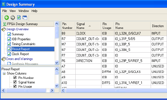

Figure 19: Package Pin Locations Prior to Pin Location Constraints (расположение выводов на корпусе ИМС до введения ограничений на их размещение).
3. Reimplement the design by double-clicking the Implement Design process (повторно реализуйте разработку за счет двойного щелчка по опции Implement Design process (процесс реализации разработки);
4. Select the Pinout Report again and select the Signal Name column header to sort the signal names (выберите опцию Pinout Report (отчет о разводке выводов) снова и выберите заголовок колонки Signal Name (имя сигнала) для сортировки имен сигналов);
5. Verify that signals are now being routed to the correct package pins (проверьте маршрутизацию сигналов согласно выбранных выводов корпуса ИМС);


Figure 20: Package Pin Locations After Pin Location Constraints (размещение выводов после введения ограничений на их размещение).
6. Close the Design Summary (закройте опцию Design Summary (итоги разработки).
Download Design to the Spartan™-3 Demo Board (Загрузите разработанную программу в Демонстрационную плату Spartan™-3 Demo Board).


7-segment LED Digit Control
VGA port - порт в видеографической матрице.
This is the last step in the design verification process. This section provides simple instructions for downloading the counter design to the Spartan-3 Starter Kit demo board.
1. Connect the 5V DC power cable to the power input on the demo board (J4).
2. Connect the download cable between the PC and demo board (J7).
3. Select Synthesis/Implementation from the drop-down list in the Sources window.
4. Select counter in the Sources window.
5. In the Processes window, click the “+” sign to expand the Generate Programming File processes.
6. Double-click the Configure Device (iMPACT) process.
7. The Xilinx WebTalk Dialog box may open during this process. Click Decline.
8. Select Disable the collection of device usage statistics for this project only and click OK.
iMPACT opens and the Configure Devices dialog box is displayed.
Этот этап является последним в процессе верификации данной структуры БМК. В данной секции приведены инструкции по загрузке разработанной Вами программы счетчика в Демонстрационную плату Spartan™-3 Demo Board.

Figure 21: iMPACT Welcome Dialog Box (Диалоговое окно iMPACT Welcome Dialog Box).
9. In the Welcome dialog box, select Configure devices using Boundary-Scan (JTAG).
10. Verify that Automatically connect to a cable and identify Boundary-Scan chain is selected.
11. Click Finish.
12. If you get a message saying that there are two devices found, click OK to continue.
The devices connected to the JTAG chain on the board will be detected and displayed in the iMPACT window.


Figure 22: Assign New Configuration File (Процесс определения Файла новой конфигурации).
14. If you get a Warning message, click OK.
15. Select Bypass to skip any remaining devices.
16. Right-click on the xc3s200 device image, and select Program... The Programming
Properties dialog box opens.
17. Click OK to program the device.
When programming is complete, the Program Succeeded message is displayed.
PROGRAM SUCCEEDED
В случае успешного завершения процесса загрузки и верификации Вашей программы Вы получаете сообщение об успешном ее завершении.
On the board, LEDs 0, 1, 2, and 3 are lit, indicating that the counter is running.
18. Close iMPACT without saving.
You have completed the ISE Quick Start Tutorial. For an in-depth explanation of the ISE design tools, see the ISE In-Depth Tutorial on the Xilinx® web site at:
[http://www.xilinx.com/support/techsup/tutorials/]
Physical Synthesis Flows for FPGA Designs