

бакМИТ_КП2015 / Компоненты по вариантам / Операционные_усилители / LT6010IDD
.pdf


 135 A, 14nV/√Hz, Rail-to-Rail Output Precision Op Amp with Shutdown
FEATURES
■35µV Maximum Offset Voltage
■110pA Maximum Input Bias Current
■135µA Supply Current
■Rail-to-Rail Output Swing
■12µA Supply Current in Shutdown
■120dB Minimum Voltage Gain (VS = ±15V)
■0.8µV/°C Maximum VOS Drift
■14nV/√Hz Input Noise Voltage
■2.7V to ±18V Supply Voltage Operation
■Operating Temperature Range: – 40°C to 85°C
■Space Saving 3mm × 3mm DFN Package
APPLICATIOUS
■Thermocouple Amplifiers
■Precision Photo Diode Amplifiers
■Instrumentation Amplifiers
■Battery-Powered Precision Systems
DESCRIPTIOU
The LT®6010 op amp combines low noise and high precision input performance with low power consumption and rail-to-rail output swing.
Input offset voltage is trimmed to less than 35µV. The low drift and excellent long-term stability guarantee a high accuracy over temperature and over time. The 110pA maximum input bias current and 120dB minimum voltage gain further maintain this precision over operating conditions.
The LT6010 works on any power supply voltage from 2.7V to 36V, and draws only 135µA of supply current on a 5V supply. A power saving shutdown feature reduces supply current to 12µA. The output voltage swings to within 40mV of either supply rail, making the amplifier a good choice for low voltage single supply operation.
The LT6010 is fully specified at 5V and ±15V supplies and from –40°C to 85°C. The device is available in SO-8 and space-saving 3mm × 3mm DFN packages. This op amp is also available in dual (LT6011) and quad (LT6012) packages.
, LTC and LT are registered trademarks of Linear Technology Corporation.
TYPICAL APPLICATIOU
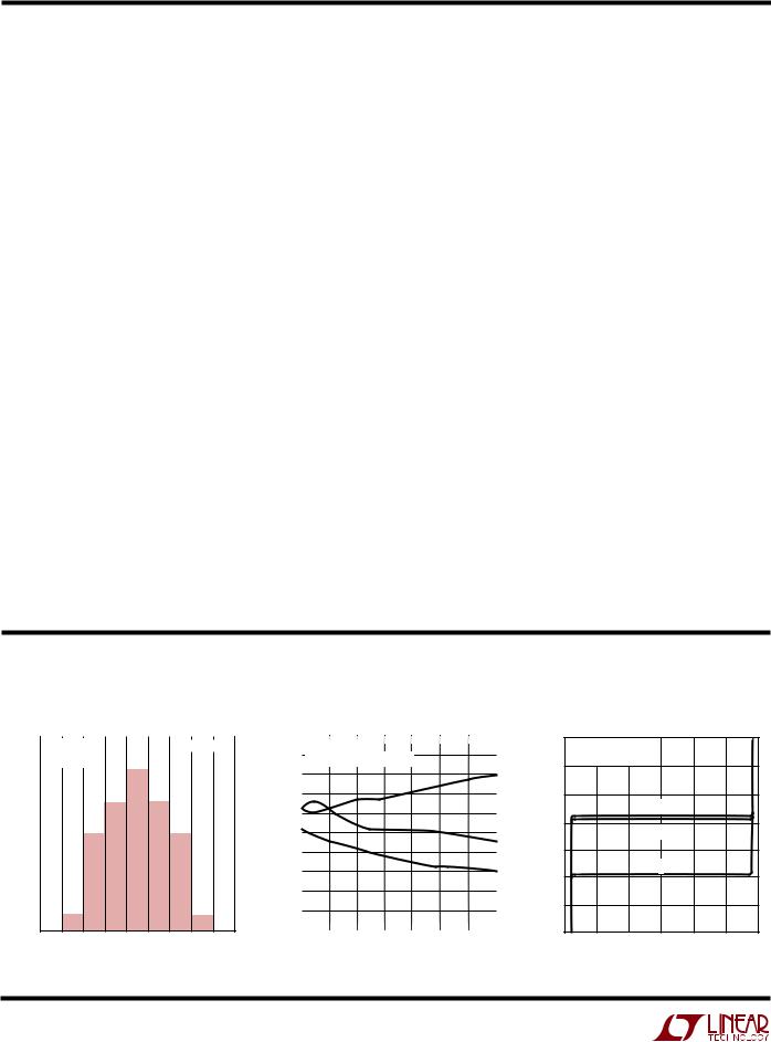
Single Supply Current Source for Platinum RTD
Distribution of Offset Voltage Drift
R5 |
|
|
|
|
|
|
|
|
20 |
|
|
|
|
|
|
1k, 5% |
|
|
|
|
|
|
|
|
= ±2.5V |
|
|
|
|
|
|
|
|
|
|
|
|
|
|
|
VS |
|
SO-8 PACKAGES |
||||
|
|
|
|
|
|
|
|
|
18 |
|
|
|
|
|
|
|
|
|
+ |
|
|
|
|
(%) |
16 |
|
|
|
|
|
|
|
|
|
VOUT = 100mV AT 0°C + 385µV/°C |
14 |
|
|
|
|
|
|
|||||
1k |
|
|
– |
–50°C TO 600°C |
|
|
UNITS |
|
|
|
|
|
|
||
RTD* |
|
|
|
|
|
|
|
12 |
|
|
|
|
|
|
|
AT 0°C |
|
|
|
|
|
|
|
|
|
|
|
|
|
|
|
|
C1 |
|
VS |
|
|
|
|
OF |
10 |
|
|
|
|
|
|
R4 |
0.1µF |
|
|
|
|
PERCENTAGE |
|
|
|
|
|
|
|||
3 |
|
|
|
|
|
|
8 |
|
|
|
|
|
|
||
1k, 5% |
2 |
– |
7 |
|
|
|
|
|
|
|
|
|
|
|
|
|
|
|
|
|
|
|
|
|
|
|
|
|
|||
R1 |
|
|
6 |
|
|
|
|
6 |
|
|
|
|
|
|
|
|
LT6010 |
|
|
|
|
|
|
|
|
|
|
||||
12.4k |
|
|
|
|
|
|
|
|
|
|
|
|
|
||
|
|
|
|
|
|
|
|
4 |
|
|
|
|
|
|
|
0.1% |
|
+ |
4 |
|
|
|
|
|
|
|
|
|
|
|
|
R2 |
|
|
|
|
|
|
|
|
|
|
|
|
|
||
|
|
|
|
|
|
|
|
2 |
|
|
|
|
|
|
|
100Ω |
|
|
|
|
|
|
|
|
|
|
|
|
|
|
|
|
|
|
|
|
|
|
|
|
|
|
|
|
|
|
|
1% |
|
|
6 |
LT1790-1.25 |
4 |
VS |
|
0 |
|
|
|
|
|
|
|
|
|
|
|
|
|
0.2 |
0.4 |
0.6 |
0.8 |
||||||
|
|
|
|
|
|
–0.8 |
–0.6 –0.4 –0.2 |
0 |
|||||||
VS = 2.7V TO 20V |
|
|
1µF |
1 |
2 |
|
|
|
|||||||
|
|
|
|
|
|
DISTRIBUTION ( V/°C) |
|
|
|||||||
|
|
|
|
|
|
|
|
|
|
|
|||||
ICC ≈ 320µA |
|
|
|
|
|
|
|
|
|
|
|
|
|
|
|
*OMEGA F3141 1kΩ , 0.1% PLATINUM RTD |
(800) 826-6342 |
|
|
|
|
|
|
|
|
6010 TA01b |
|||||
|
|
|
|
|
|
|
|
|
|
||||||
|
|
|
|
|
6010 TA01a |
|
|
|
|
|
|
|
|
|
|
sn6010 6010fs
1

LT6010
ABSOLUTE
WAXIWUW
RATIUGS (Note 1)
Total Supply Voltage (V+ to V–) .............................. |
40V |
Maximum Junction Temperature |
125°C |
Differential Input Voltage (Note 2) .......................... |
10V |
DD Package ..................................................... |
|
Input Voltage, Shutdown Voltage ..................... |
V+ to V– |
SO-8 Package .................................................. |
150°C |
Input Current (Note 2) ....................................... |
±10mA |
Storage Temperature Range |
– 65°C to 125°C |
Output Short-Circuit Duration (Note 3) ........... |
Indefinite |
DD Package ..................................... |
|
Operating Temperature Range (Note 4) .. |
– 40°C to 85°C |
SO-8 Package .................................. |
– 65°C to 150°C |
Specified Temperature Range (Note 5) ... |
– 40°C to 85°C |
Lead Temperature (Soldering, 10 sec).................. |
300°C |
|
|
|
|
|
|
|
|
PACKAGE/ORDER IUFORWATIOU
TOP VIEW
NULL |
1 |
|
8 |
NULL |
–IN |
2 |
– |
7 |
V+ |
+IN |
3 |
+ |
6 |
OUT |
|
||||
V– |
4 |
|
5 |
SHDN |
DD PACKAGE
8-LEAD (3mm × 3mm) PLASTIC DFN
TJMAX = 125°C, θJA = 160°C/W
UNDERSIDE METAL INTERNALLY CONNECTED TO V–
(PCB CONNECTION OPTIONAL)
ORDER PART
NUMBER
LT6010CDD
LT6010IDD
LT6010ACDD
LT6010AIDD
DD PART MARKING*
LADU
TOP VIEW
NULL |
1 |
|
8 |
NULL |
–IN |
2 |
– |
7 |
V+ |
+IN |
3 |
+ |
6 |
OUT |
|
||||
V– |
4 |
|
5 |
SHDN |
S8 PACKAGE
8-LEAD PLASTIC SO
TJMAX = 150°C, θJA = 190°C/W
ORDER PART
NUMBER
LT6010CS8
LT6010IS8
LT6010ACS8
LT6010AIS8
S8 PART MARKING
6010
6010I
6010A
6010AI
*Temperature grades are identified by a label on the shipping container. Consult LTC Marketing for parts specified with wider operating temperature ranges.
ELECTRICAL CHARACTERISTICS The ● denotes the specifications which apply over the full operating temperature range, otherwise specifications are at TA = 25°C. VS = 5V, 0V; VCM = 2.5V; RL to 0V; SHDN = 0.2V, unless otherwise specified. (Note 5)
SYMBOL |
PARAMETER |
CONDITIONS |
|
MIN |
TYP |
MAX |
UNITS |
|
|
|
|
|
|
|
|
VOS |
Input Offset Voltage (Note 7) |
LT6010AS8 |
|
|
10 |
35 |
µV |
|
|
TA = 0°C to 70°C |
● |
|
|
60 |
µV |
|
|
TA = –40°C to 85°C |
● |
|
|
75 |
µV |
|
|
LT6010S8 |
|
|
20 |
55 |
µV |
|
|
TA = 0°C to 70°C |
● |
|
|
85 |
µV |
|
|
TA = –40°C to 85°C |
● |
|
|
110 |
µV |
|
|
LT6010ADD |
|
|
20 |
60 |
µV |
|
|
TA = 0°C to 70°C |
● |
|
|
85 |
µV |
|
|
TA = –40°C to 85°C |
● |
|
|
100 |
µV |
|
|
LT6010DD |
|
|
30 |
80 |
µV |
|
|
TA = 0°C to 70°C |
● |
|
|
110 |
µV |
|
|
TA = –40°C to 85°C |
● |
|
|
135 |
µV |
VOS/ T |
Input Offset Voltage Drift (Note 6) |
LT6010AS8, LT6010S8 |
● |
|
0.2 |
0.8 |
µV/°C |
|
|
LT6010ADD,LT6010DD |
● |
|
0.2 |
1.3 |
µV/°C |
sn6010 6010fs
2

LT6010
temperature range, otherwise specifications are at TA specified. (Note 5)
The ● denotes the specifications which apply over the full operating = 25°C. VS = 5V, 0V; VCM = 2.5V; RL to 0V; SHDN = 0.2V, unless otherwise
SYMBOL |
PARAMETER |
CONDITIONS |
|
MIN |
TYP |
MAX |
UNITS |
|
||
|
|
|
|
|
|
|
|
|
|
|
IOS |
Input Offset Current (Note 7) |
LT6010AS8 |
|
|
20 |
110 |
|
pA |
||
|
|
TA = 0°C to 70°C |
● |
|
|
150 |
|
pA |
||
|
|
TA = –40°C to 85°C |
● |
|
|
200 |
|
pA |
|
|
|
|
LT6010S8 |
|
|
40 |
200 |
|
pA |
||
|
|
TA = 0°C to 70°C |
● |
|
|
300 |
|
pA |
||
|
|
TA = –40°C to 85°C |
● |
|
|
400 |
|
pA |
|
|
|
|
LT6010ADD |
|
|
20 |
200 |
|
pA |
||
|
|
TA = 0°C to 70°C |
● |
|
|
300 |
|
pA |
||
|
|
TA = –40°C to 85°C |
● |
|
|
400 |
|
pA |
|
|
|
|
LT6010DD |
|
|
40 |
300 |
|
pA |
||
|
|
TA = 0°C to 70°C |
● |
|
|
400 |
|
pA |
||
|
|
TA = –40°C to 85°C |
● |
|
|
500 |
|
pA |
|
|
IB |
Input Bias Current (Note 7) |
LT6010AS8 |
|
|
20 |
±110 |
|
pA |
||
|
|
TA = 0°C to 70°C |
● |
|
|
±150 |
|
pA |
||
|
|
TA = –40°C to 85°C |
● |
|
|
±200 |
|
pA |
|
|
|
|
LT6010S8 |
|
|
40 |
±200 |
|
pA |
||
|
|
TA = 0°C to 70°C |
● |
|
|
±300 |
|
pA |
||
|
|
TA = –40°C to 85°C |
● |
|
|
±400 |
|
pA |
|
|
|
|
LT6010ADD |
|
|
20 |
±200 |
|
pA |
||
|
|
TA = 0°C to 70°C |
● |
|
|
±300 |
|
pA |
||
|
|
TA = –40°C to 85°C |
● |
|
|
±400 |
|
pA |
|
|
|
|
LT6010DD |
|
|
40 |
±300 |
|
pA |
||
|
|
TA = 0°C to 70°C |
● |
|
|
±400 |
|
pA |
||
|
|
TA = –40°C to 85°C |
● |
|
|
±500 |
|
pA |
|
|
|
Input Noise Voltage |
0.1Hz to 10Hz |
|
|
400 |
|
nVP-P |
|
||
en |
Input Noise Voltage Density |
f = 1kHz |
|
|
14 |
|
nV/√ |
|
|
|
|
|
|
Hz |
|||||||
in |
Input Noise Current Density |
f = 1kHz |
|
|
0.1 |
|
pA/√ |
|
|
|
|
|
|
Hz |
|||||||
RIN |
Input Resistance |
Common Mode, VCM = 1V to 3.8V |
|
10 |
120 |
|
GΩ |
|||
|
|
Differential |
|
|
20 |
|
MΩ |
|
||
CIN |
Input Capacitance |
|
|
|
4 |
|
|
pF |
|
|
VCM |
Input Voltage Range (Positive) |
Guaranteed by CMRR |
● |
3.8 |
4 |
|
|
V |
||
|
Input Voltage Range (Negative) |
Guaranteed by CMRR |
● |
|
0.7 |
1 |
|
V |
|
|
CMRR |
Common Mode Rejection Ratio |
VCM = 1V to 3.8V |
● |
107 |
135 |
|
|
dB |
|
|
|
Minimum Supply Voltage |
Guaranteed by PSRR |
● |
|
2.4 |
2.7 |
|
V |
||
|
|
|
|
|
|
|
|
|
|
|
PSRR |
Power Supply Rejection Ratio |
VS = 2.7V to 36V, VCM = 1/2VS |
● |
112 |
135 |
|
|
dB |
|
|
AVOL |
Large-Signal Voltage Gain |
RL = 10k, VOUT = 1V to 4V |
● |
300 |
2000 |
|
V/mV |
|||
|
|
RL = 2k, VOUT = 1V to 4V |
● |
250 |
2000 |
|
V/mV |
|
||
VOUT |
Maximum Output Swing |
No Load, 50mV Overdrive |
|
|
35 |
55 |
mV |
|||
|
(Positive, Referred to V+) |
|
● |
|
|
65 |
mV |
|
||
|
|
ISOURCE = 1mA, 50mV Overdrive |
|
|
120 |
170 |
mV |
|||
|
|
|
● |
|
|
220 |
mV |
|
||
|
Maximum Output Swing |
No Load, 50mV Overdrive |
|
|
40 |
55 |
mV |
|||
|
(Negative, Referred to 0V) |
|
● |
|
|
65 |
mV |
|||
|
|
|
|
|
|
|
|
|
|
|
|
|
ISINK = 1mA, 50mV Overdrive |
|
|
150 |
225 |
mV |
|||
|
|
|
● |
|
|
275 |
mV |
|
||
sn6010 6010fs
3

The ● denotes the specifications which apply over the full operating = 25°C. VS = 5V, 0V; VCM = 2.5V; RL to 0V; SHDN = 0.2V, unless otherwise
SYMBOL |
PARAMETER |
CONDITIONS |
|
MIN |
TYP |
MAX |
UNITS |
|
|
|
|
|
|
|
|
ISC |
Output Short-Circuit Current (Note 3) |
VOUT = 0V, 1V Overdrive (Source) |
|
10 |
14 |
|
mA |
|
|
|
● |
4 |
|
|
mA |
|
|
|
|
|
|
|
|
|
|
VOUT = 5V, –1V Overdrive (Sink) |
|
10 |
21 |
|
mA |
|
|
|
● |
4 |
|
|
mA |
SR |
Slew Rate |
AV = –10, RF = 50k, RG = 5k |
|
0.06 |
0.09 |
|
V/µs |
|
|
TA = 0°C to 70°C |
● |
0.05 |
|
|
V/µs |
|
|
TA = –40°C to 85°C |
● |
0.04 |
|
|
V/µs |
GBW |
Gain Bandwidth Product |
f = 10kHz |
|
250 |
330 |
|
kHz |
|
|
|
● |
225 |
|
|
kHz |
ts |
Settling Time |
AV = –1, 0.01%, VOUT = 1.5V to 3.5V |
|
|
45 |
|
µs |
tr, tf |
Rise Time, Fall Time |
AV = 1, 10% to 90%, 0.1V Step |
|
|
1 |
|
µs |
ISHDN |
SHDN Pin Current |
SHDN ≤ V– + 0.2V (On) |
● |
|
|
0.25 |
µA |
|
|
SHDN = V– + 2.0V (Off) |
● |
|
15 |
25 |
µA |
tSHDN |
SHDN Turn-On, Turn-Off Time |
SHDN = V– (On) to V– + 2.0V (Off) |
|
|
25 |
|
µs |
|
|
SHDN = V– + 2.0V (Off) to V– (On) |
|
|
25 |
|
µs |
IS |
Supply Current |
SHDN ≤ V– + 0.2V (On) |
|
|
135 |
150 |
µA |
|
|
TA = 0°C to 70°C |
● |
|
|
190 |
µA |
|
|
TA = –40°C to 85°C |
● |
|
|
210 |
µA |
|
|
SHDN = V– + 2.0V (Off) |
|
|
12 |
25 |
µA |
|
|
|
● |
|
|
50 |
µA |
The ● denotes the specifications which apply over the full operating temperature range, otherwise specifications are at TA = 25°C. VS = ±15V, VCM = 0V, RL to 0V; SHDN = –14.8V, unless otherwise specified. (Note 5)
SYMBOL |
PARAMETER |
CONDITIONS |
|
MIN |
TYP |
MAX |
UNITS |
|
|
|
|
|
|
|
|
|
|
VOS |
Input Offset Voltage (Note 7) |
LT6010AS8 |
|
|
10 |
60 |
µV |
|
|
|
|
TA = 0°C to 70°C |
● |
|
|
80 |
µV |
|
|
|
TA = –40°C to 85°C |
● |
|
|
110 |
µV |
|
|
|
LT6010S8 |
|
|
20 |
85 |
µV |
|
|
|
TA = 0°C to 70°C |
● |
|
|
120 |
µV |
|
|
|
TA = –40°C to 85°C |
● |
|
|
160 |
µV |
|
|
|
LT6010ADD |
|
|
20 |
85 |
µV |
|
|
|
TA = 0°C to 70°C |
● |
|
|
105 |
µV |
|
|
|
TA = –40°C to 85°C |
● |
|
|
135 |
µV |
|
|
|
LT6010DD |
|
|
30 |
110 |
µV |
|
|
|
TA = 0°C to 70°C |
● |
|
|
145 |
µV |
|
|
|
TA = –40°C to 85°C |
● |
|
|
185 |
µV |
VOS/ T |
Input Offset Voltage Drift (Note 6) |
LT6010AS8, LT6010S8 |
● |
|
0.2 |
0.8 |
µV/°C |
|
|
|
|
LT6010ADD,LT6010DD |
● |
|
0.2 |
1.3 |
µV/°C |
IOS |
Input Offset Current (Note 7) |
LT6010AS8 |
|
|
20 |
110 |
pA |
|
|
|
|
TA = 0°C to 70°C |
● |
|
|
150 |
pA |
|
|
|
TA = –40°C to 85°C |
● |
|
|
200 |
pA |
|
|
|
LT6010S8 |
|
|
40 |
200 |
pA |
|
|
|
TA = 0°C to 70°C |
● |
|
|
300 |
pA |
|
|
|
TA = –40°C to 85°C |
● |
|
|
400 |
pA |
|
|
|
LT6010ADD |
|
|
20 |
200 |
pA |
|
|
|
TA = 0°C to 70°C |
● |
|
|
300 |
pA |
|
|
|
TA = –40°C to 85°C |
● |
|
|
400 |
pA |
sn6010 6010fs
4

LT6010
ELECTRICAL CHARACTERISTICS The ● denotes the specifications which apply over the full operating temperature range, otherwise specifications are at TA = 25°C. VS = ±15V, VCM = 0V, RL to 0V; SHDN = –14.8V, unless otherwise specified. (Note 5)
SYMBOL |
PARAMETER |
CONDITIONS |
|
MIN |
TYP |
MAX |
UNITS |
|||
|
|
|
|
|
|
|
|
|
|
|
IOS |
Input Offset Current (Note 7) |
LT6010DD |
|
|
40 |
300 |
|
pA |
||
|
|
TA = 0°C to 70°C |
● |
|
|
400 |
|
pA |
||
|
|
TA = –40°C to 85°C |
● |
|
|
500 |
|
pA |
||
IB |
Input Bias Current (Note 7) |
LT6010AS8 |
|
|
20 |
±110 |
|
pA |
||
|
|
TA = 0°C to 70°C |
● |
|
|
±150 |
|
pA |
||
|
|
TA = –40°C to 85°C |
● |
|
|
±200 |
|
pA |
||
|
|
LT6010S8 |
|
|
40 |
±200 |
|
pA |
||
|
|
TA = 0°C to 70°C |
● |
|
|
±300 |
|
pA |
||
|
|
TA = –40°C to 85°C |
● |
|
|
±400 |
|
pA |
||
|
|
LT6010ADD |
|
|
20 |
±200 |
|
pA |
||
|
|
TA = 0°C to 70°C |
● |
|
|
±300 |
|
pA |
||
|
|
TA = –40°C to 85°C |
● |
|
|
±400 |
|
pA |
||
|
|
LT6010DD |
|
|
40 |
±300 |
|
pA |
||
|
|
TA = 0°C to 70°C |
● |
|
|
±400 |
|
pA |
||
|
|
TA = –40°C to 85°C |
● |
|
|
±500 |
|
pA |
||
|
Input Noise Voltage |
0.1Hz to 10Hz |
|
|
400 |
|
nVP-P |
|||
en |
Input Noise Voltage Density |
f = 1kHz |
|
|
13 |
|
nV/√ |
|
|
|
|
|
|
Hz |
|||||||
in |
Input Noise Current Density |
f = 1kHz |
|
|
0.1 |
|
pA/√ |
|
|
|
|
|
|
Hz |
|||||||
RIN |
Input Resistance |
Common Mode, VCM = ±13.5V |
|
50 |
400 |
|
G Ω |
|||
|
|
Differential |
|
|
20 |
|
MΩ |
|||
CIN |
Input Capacitance |
|
|
|
4 |
|
|
|
pF |
|
VCM |
Input Voltage Range |
Guaranteed by CMRR |
● |
±13.5 |
±14 |
|
|
|
V |
|
CMRR |
Common Mode Rejection Ratio |
VCM = –13.5V to 13.5V |
|
115 |
135 |
|
|
dB |
||
|
|
|
● |
112 |
|
|
|
dB |
||
|
Minimum Supply Voltage |
Guaranteed by PSRR |
● |
|
±1.2 |
±1.35 |
|
|
V |
|
|
|
|
|
|
|
|
|
|
|
|
PSRR |
Power Supply Rejection Ratio |
VS = ±1.35V to ±18V |
● |
112 |
135 |
|
|
dB |
||
AVOL |
Large-Signal Voltage Gain |
RL = 10k, VOUT = –13.5V to 13.5V |
|
1000 |
2000 |
|
V/mV |
|||
|
|
|
● |
600 |
|
|
V/mV |
|||
|
|
RL = 5k, VOUT = –13.5V to 13.5V |
|
500 |
1500 |
|
V/mV |
|||
|
|
|
● |
300 |
|
|
V/mV |
|||
VOUT |
Maximum Output Swing |
No Load, 50mV Overdrive |
|
|
45 |
80 |
mV |
|||
|
(Positive, Referred to V+) |
|
● |
|
|
100 |
mV |
|||
|
|
ISOURCE = 1mA, 50mV Overdrive |
|
|
140 |
195 |
mV |
|||
|
|
|
● |
|
|
240 |
mV |
|||
|
Maximum Output Swing |
No Load, 50mV Overdrive |
|
|
45 |
80 |
mV |
|||
|
(Negative, Referred to 0V) |
|
● |
|
|
100 |
mV |
|||
|
|
|
|
|
|
|
|
|
|
|
|
|
ISINK = 1mA, 50mV Overdrive |
|
|
150 |
250 |
mV |
|||
|
|
|
● |
|
|
300 |
mV |
|||
ISC |
Output Short-Circuit Current (Note 3) |
VOUT = 0V, 1V Overdrive (Source) |
|
10 |
15 |
|
mA |
|||
|
|
|
● |
5 |
|
|
mA |
|||
|
|
VOUT = 0V, –1V Overdrive (Sink) |
|
10 |
20 |
|
mA |
|||
|
|
|
● |
5 |
|
|
mA |
|||
sn6010 6010fs
5
The ● denotes the specifications which apply over the full operating = 25°C. VS = ±15V, VCM = 0V, RL to 0V; SHDN = –14.8V, unless otherwise
SYMBOL |
PARAMETER |
CONDITIONS |
|
MIN |
TYP |
MAX |
UNITS |
|
|
|
|
|
|
|
|
SR |
Slew Rate |
AV = –10, RF = 50k, RG = 5k |
|
0.08 |
0.11 |
|
V/ s |
|
|
TA = 0°C to 70°C |
● |
0.07 |
|
|
V/ s |
|
|
TA = –40°C to 85°C |
● |
0.05 |
|
|
V/ s |
GBW |
Gain Bandwidth Product |
f = 10kHz |
|
275 |
350 |
|
kHz |
|
|
|
● |
250 |
|
|
kHz |
|
|
|
|
|
|
|
|
ts |
Settling Time |
AV = –1, 0.01%, VOUT = 0V to 10V |
|
|
85 |
|
s |
tr, tf |
Rise Time, Fall Time |
AV = 1, 10% to 90%, 0.1V Step |
|
|
1 |
|
s |
ISHDN |
SHDN Pin Current |
SHDN ≤ V– + 0.2V (On) |
● |
|
|
0.25 |
A |
|
|
SHDN = V– + 2.0V (Off) |
● |
|
15 |
25 |
A |
tSHDN |
SHDN Turn-On, Turn-Off Time |
SHDN = V– (On) to V– + 2.0V (Off) |
|
|
25 |
|
s |
|
|
SHDN = V– + 2.0V (Off) to V– (On) |
|
|
25 |
|
s |
IS |
Supply Current |
SHDN ≤ V– + 0.2V (On) |
|
|
260 |
330 |
A |
|
|
TA = 0°C to 70°C |
● |
|
|
380 |
A |
|
|
TA = –40°C to 85°C |
● |
|
|
400 |
A |
|
|
SHDN = V– + 2.0V (Off) |
|
|
18 |
50 |
A |
Note 1: Absolute Maximum Ratings are those beyond which the life of the device may be impaired.
Note 2: The inputs are protected by back–to–back diodes and internal series resistors. If the differential input voltage exceeds 10V, the input current must be limited to less than 10mA.
Note 3: A heat sink may be required to keep the junction temperature below absolute maximum ratings.
Note 4: Both the LT6010C and LT6010I are guaranteed functional over the operating temperature range of –40°C to 85°C.
Note 5: The LT6010C is guaranteed to meet the specified performance
from 0°C to 70°C and is designed, characterized and expected to meet specified performance from –40°C to 85°C but is not tested or QA sampled at these temperatures. The LT6010I is guaranteed to meet specified performance from –40°C to 85°C.
Note 6: This parameter is not 100% tested.
Note 7: The specifications for VOS, IB and IOS depend on the grade and on the package. The following table clarifies the notations used in the specification table:
|
Standard Grade |
A Grade |
|
|
|
S8 Package |
LT6010S8 |
LT6010AS8 |
|
|
|
DFN Package |
LT6010DD |
LT6010ADD |
|
|
|
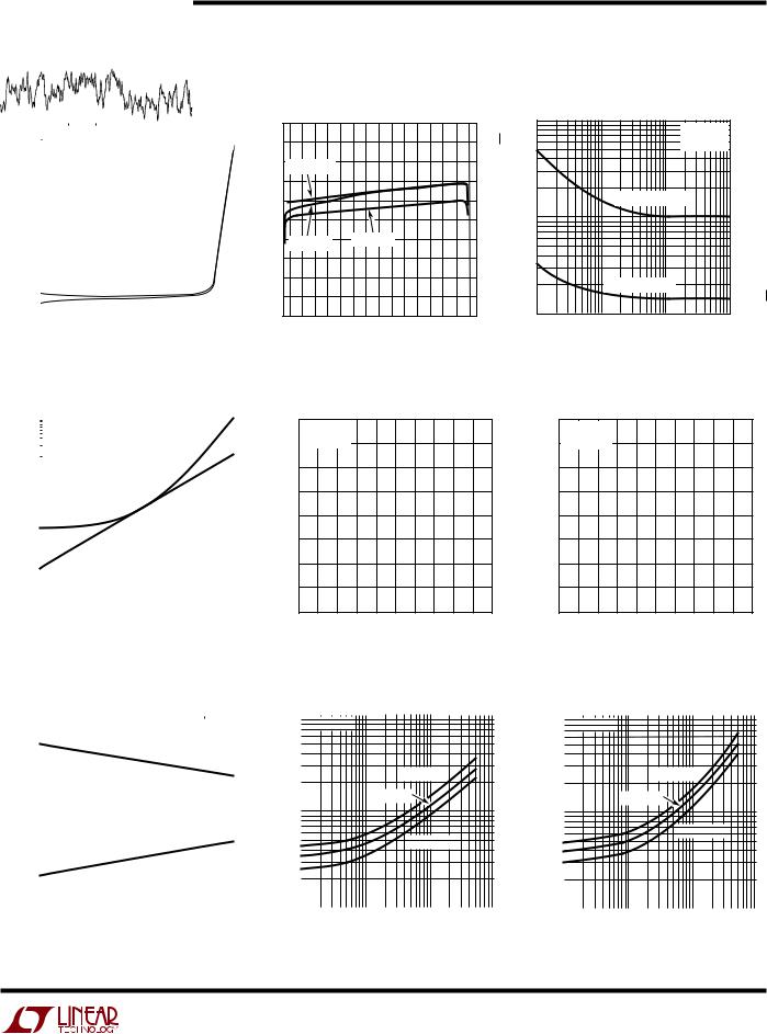
TYPICAL PERFORWAUCE CHARACTERISTICS
Distribution of Input Offset Voltage
|
30 |
|
|
|
|
|
|
|
|
|
|
|
|
|
|
|
|
|
|
|
|
|
|
|
|
|
|
|
|
VS = 5V, 0V |
|
|
|
|
LT6010AS8 |
|
|||||
|
|
|
|
|
|
|
|
||||||
(%) |
25 |
|
TA = 25°C |
|
|
|
|
|
|
|
|
||
20 |
|
|
|
|
|
|
|
|
|
|
|
|
|
UNITS |
15 |
|
|
|
|
|
|
|
|
|
|
|
|
OF |
|
|
|
|
|
|
|
|
|
|
|
|
|
PERCENT |
10 |
|
|
|
|
|
|
|
|
|
|
|
|
|
|
|
|
|
|
|
|
|
|
|
|
|
|
|
5 |
|
|
|
|
|
|
|
|
|
|
|
|
|
|
|
|
|
|
|
|
|
|
|
|
|
|
|
|
|
|
|
|
|
|
|
|
|
|
|
|
0 –45 –35 –25 –15 –5 5 15 25 35 45
INPUT OFFSET VOLTAGE ( V)
6010 G01
6
Input Offset Voltage vs Temperature
|
125 |
|
|
VS = 5V, 0V |
|
|
100 |
|
|
REPRESENTATIVE UNITS |
|
|
|
|
(V) |
75 |
|
50 |
|
|
VOLTAGE |
|
|
25 |
|
|
|
|
|
|
0 |
|
OFFSET |
–25 |
|
–50 |
|
|
|
|
|
|
–75 |
|
|
–100 |
|
|
–125 |
|
|
|
–50 –25 0 25 50 75 100 125 TEMPERATURE (°C)
6010 G02
OFFSET VOLTAGE ( V)
Offset Voltage
vs Input Common Mode Voltage
120
VS = ±15V
TYPICAL PART
100
80
TA = 85°C
60
TA = –40°C
40
TA = 25°C
20
0
–20 –15 –10 –5 0 5 10 15
INPUT COMMON MODE VOLTAGE (V)
6010 G03
sn6010 6010fs
LT6010
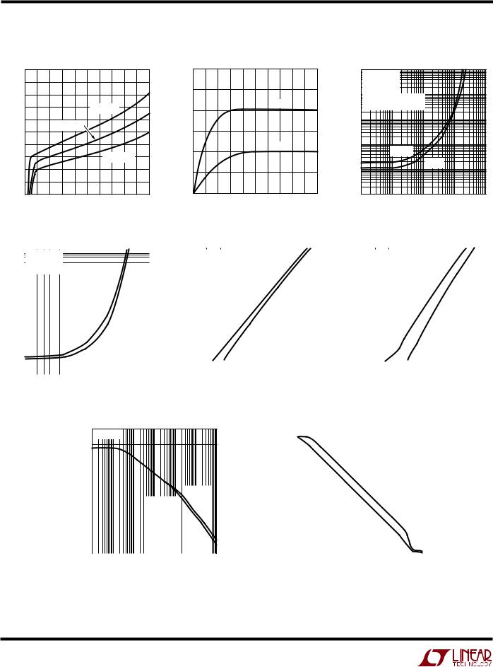
TYPICAL PERFORWAUCE CHARACTERISTICS
INPUT BIAS CURRENT (pA)
Input Bias Current vs Temperature
1000 |
|
|
|
|
|
|
|
|
VS = 5V, 0V |
|
|
|
|
|
|||
900 |
|
|
|
|
|
|||
TYPICAL PART |
|
|
|
|
|
|||
|
|
|
|
|
|
|||
800 |
|
|
|
|
|
|
|
|
|
|
|
|
|
|
|
|
|
700 |
|
|
|
|
|
|
|
|
|
|
|
|
|
|
|
|
|
600 |
|
|
|
|
|
|
|
|
|
|
|
|
|
|
|
|
|
500 |
|
|
|
|
|
|
|
|
|
|
|
|
|
|
|
|
|
400 |
|
|
|
|
|
|
|
|
|
|
|
|
|
|
|
|
|
300 |
|
|
|
|
|
|
|
|
|
|
|
|
|
|
|
|
|
200 |
|
|
|
|
|
|
|
|
|
|
|
|
|
|
|
|
|
100 |
|
|
|
|
|
|
|
|
|
IB+ |
|
|
|
|
|
|
|
0 |
|
|
|
|
|
|
||
|
IB– |
|
|
|
|
|
|
|
–100 |
|
|
|
|
|
|
||
|
|
|
|
|
|
|
|
|
–50 –25 0 25 50 75 100 125 TEMPERATURE (°C)
6010 G04
Input Bias Current |
en, in vs Frequency |
vs Input Common Mode Voltage |
100 |
|
|
|
|
|
1000 |
20pA/DIV |
|
|
NOISEVOLTAGEINPUTDENSITY (nV/√Hz) |
|
|
VS = ±15V |
|
|
|
|
Hz)(fA/DENSITYNOISE√ CURRENTINPUT |
||
|
|
|
|
|
|
TA = 25°C |
TA = –40°C |
|
|
|
|
|
|
|
|
|
|
|
CURRENT NOISE |
|
|
|
|
100 |
|
|
100 |
TA = 85°C |
TA = 25°C |
|
|
|
|
|
|
|
|
|
VOLTAGE NOISE |
|
|
–100 |
|
|
10 |
10 |
100 |
1000 |
–15 |
2V/DIV |
15 |
1 |
|||
|
|
|
|
FREQUENCY (Hz) |
|
|
|
|
6010 G05 |
|
|
|
6010 G06 |
|
|
|
|
|
|
|
Total Input Noise
vs Source Resistance
|
|
|
10 |
|
|
|
|
|
|
|
|
|
|
|
|
|
|
|
|
|
|
|
|
|
|
|
|
|
|
|
|
|
|
|
|
|
|
|
|
|
|
VS = 5V, 0V |
|
|
|
|
|
|
|
|
|
|
|
|
|
|
|
|
|
|
|
|
|
|
|
|
|||||||
|
|
|
|
|
|
|
|
|
|
|
|
|
|
|
|
|
|
|
|
|
|
|
|
|
|
|
|
|
||||||||
|
|
|
|
|
TA = 25°C |
|
|
|
|
|
|
|
|
|
|
|
|
|
|
|
|
|
|
|
|
|
|
|
|
|||||||
|
|
|
|
|
|
|
|
|
|
|
|
|
|
|
|
|
|
|
|
|
|
|
|
|
|
|
|
|
||||||||
|
|
√Hz) |
1 |
|
f = 1kHz |
|
|
|
|
|
|
|
|
|
|
|
|
|
|
|
|
|
|
|
|
|
|
|
|
|||||||
( V/ |
0.1 |
|
|
|
|
|
|
|
|
|
|
|
|
|
|
|
|
|
|
|
|
|
|
|
|
|
|
|
|
|
|
|
|
|
||
|
|
|
|
|
|
|
|
|
|
|
|
|
|
|
|
|
|
|
|
|
|
|
|
|
|
|
|
|
|
|
|
|
||||
|
|
NOISE |
|
|
|
|
|
|
|
|
|
|
|
|
|
|
|
|
|
|
|
|
|
|
|
|
|
|
|
|
|
|
|
|
|
|
|
|
|
|
|
|
|
|
|
|
|
|
|
|
|
|
|
|
|
|
|
|
|
|
|
|
|
|
|
|
|
|
|
|
|||
|
|
|
|
|
|
|
|
|
|
|
|
|
|
|
|
|
|
|
|
|
|
|
|
|
|
|
|
|
|
|
|
|
|
|||
|
|
|
|
|
|
|
|
|
|
|
|
|
|
|
|
|
|
|
|
|
|
|
|
|
|
|
|
|
|
|
|
|
|
|
|
|
|
|
|
|
|
|
|
|
|
|
|
|
|
|
|
|
|
|
|
|
|
|
|
|
|
|
|
|
|
|
|
|
|
|
|||
|
|
|
TOTAL NOISE |
|
|
|
|
|
|
|
|
|
|
|
|
|
|
|
|
|
|
|
|
|
|
|||||||||||
|
|
|
|
|
|
|
|
|
|
|
|
|
|
|
|
|
|
|
|
|
|
|
|
|
||||||||||||
|
|
|
|
|
|
|
|
|
|
|
|
|
|
|
|
|
|
|
|
|
|
|
|
|
||||||||||||
|
|
INPUT |
0.01 |
|
|
|
|
|
|
|
|
|
|
|
|
|
|
|
|
|
|
|
|
|
|
|
|
|
|
|
|
|
|
|
|
|
|
|
|
|
|
|
|
|
|
|
|
|
|
|
|
|
|
|
|
|
|
|
|
|
|
|
|
|
|
|
|
|
|
|
|
||
|
|
|
|
|
|
|
|
|
|
|
|
|
|
|
|
|
|
|
|
|
|
|
|
|
|
|
|
|
|
|
|
|
|
|
|
|
|
|
|
|
|
|
|
|
|
|
|
|
|
|
|
|
|
|
|
|
|
|
|
|
|
|
|
|
|
|
|
|
|
|
|
||
|
|
|
|
|
|
|
|
|
|
|
|
|
|
|
|
|
|
|
|
|
|
|
|
|
|
|
|
|
|
|
|
|
|
|
|
|
|
|
TOTAL |
0.001 |
|
|
|
|
|
|
|
|
|
RESISTOR NOISE ONLY |
|
|
|
|
|
|
|
|
|||||||||||||||
|
|
|
|
|
|
|
|
|
|
|
|
|
|
|
|
|
|
|
||||||||||||||||||
|
|
|
|
|
|
|
|
|
|
|
|
|
|
|
|
|
|
|
||||||||||||||||||
|
|
|
|
|
|
|
|
|
|
|
|
|
|
|
|
|
|
|
|
|
|
|
|
|
|
|
|
|
|
|
|
|
|
|
||
|
|
|
|
|
|
|
|
|
|
|
|
|
|
|
|
|
|
|
|
|
|
|
|
|
|
|
|
|
|
|
|
|
||||
|
|
|
|
|
|
|
|
|
|
|
|
|
|
|
|
|
|
|
|
|
|
|
|
|
|
|
|
|
|
|
|
|||||
|
|
|
|
|
|
|
|
|
|
|
|
|
|
|
|
|
|
|
|
|
|
|
|
|
|
|
|
|
|
|
|
|||||
|
|
|
|
|
|
|
|
|
|
|
|
|
|
|
|
|
|
|
|
|
|
|
|
|
|
|
|
|
|
|
|
|||||
0.0001 |
|
|
|
|
|
|
|
|
|
|
|
|
|
|
|
|
|
|
|
|
|
|
|
|
|
|
|
|
|
|
|
|
|
|||
|
|
|
|
|
|
|
|
|
|
|
|
|
|
|
|
|
|
|
|
|
|
|
|
|
|
|
|
|
|
|
|
|
||||
|
|
|
|
|
|
|
|
|
|
|
|
|
|
|
|
|
|
|
|
|
|
|
|
|
|
|
|
|
|
|
|
|
||||
|
|
|
|
|
|
|
|
|
|
|
|
|
|
|
|
|
|
|
|
|
|
|
|
|
|
|
|
|
|
|
|
|
||||
|
|
|
|
|
|
|
|
|
|
|
|
|
|
|
|
|
|
|
|
|
|
|
|
|
|
|
|
|
|
|
|
|
||||
|
|
|
|
|
|
|
|
|
|
|
|
|
|
|
|
|
|
|
|
|
|
|
|
|
|
|
|
|
|
|
|
|
||||
|
|
|
|
|
|
|
|
|
|
|
|
|
|
|
|
|
|
|
|
|
|
|
|
|
|
|
|
|
100M |
|||||||
|
|
|
100 |
|
|
|
1k |
|
10k |
|
|
100k |
1M |
10M |
||||||||||||||||||||||
|
|
|
|
|
|
|
|
|
|
|
SOURCE RESISTANCE (Ω ) |
|
|
|
|
|
|
|
|
|||||||||||||||||
|
|
|
|
|
|
|
|
|
|
|
|
|
|
|
|
|
|
|
|
|
|
|
|
|
|
|
|
|
|
|
6010 G07 |
|||||
|
|
|
|
Output Voltage Swing |
|
|
|
|
|
|
|
|
|
|
|
|
|
|||||||||||||||||||
|
|
|
|
vs Temperature |
|
|
|
|
|
|
|
|
|
|
|
|
|
|||||||||||||||||||
|
|
|
V+ |
|
|
|
|
|
|
|
|
|
|
|
|
|
|
|
|
|
|
|
|
|
|
|
|
|
|
|
|
|
|
|
|
|
|
|
|
|
|
|
|
|
|
|
|
|
|
|
|
|
|
|
|
|
|
|
|
|
|
VS = 5V, 0V |
|
||||||||||
|
|
|
|
|
|
|
|
|
|
|
|
|
|
|
|
|
|
|
|
|
|
|
|
|
|
|
||||||||||
|
|
(mV) |
–20 |
|
|
|
|
|
|
|
|
|
|
|
|
|
|
|
|
|
|
|
|
|
|
NO LOAD |
|
|
|
|||||||
|
|
|
|
|
|
|
|
|
|
|
|
|
|
|
|
|
|
|
|
|
|
|
|
|
|
|
||||||||||
|
|
|
|
|
|
|
|
|
|
|
|
|
|
|
|
|
|
|
|
|
|
|
|
|
|
|
|
|
|
|
|
|
|
|
||
|
|
–40 |
|
|
|
|
|
|
|
|
|
|
|
|
|
|
|
|
|
|
|
|
|
|
|
|
|
|
|
|
|
|
|
|
|
|
|
|
|
|
|
|
|
|
|
|
|
|
|
|
|
|
|
|
|
|
|
|
|
|
|
|
|
|
|
|
|
|
|
|
|
||
|
|
SWINGVOLTAGE |
|
|
|
|
|
|
|
|
|
|
OUTPUT HIGH |
|
|
|
|
|
|
|
|
|
|
|
|
|||||||||||
|
|
60 |
|
|
|
|
|
|
|
|
|
|
|
|
|
|
|
|
|
|
|
|
|
|
||||||||||||
|
|
|
|
|
|
|
|
|
|
|
|
|
|
|
|
|
|
|
|
|
|
|
|
|||||||||||||
|
|
|
–60 |
|
|
|
|
|
|
|
|
|
|
|
|
|
|
|
|
|
|
|
|
|
|
|
|
|
|
|
|
|
|
|
|
|
|
|
|
|
|
|
|
|
|
|
|
|
|
|
|
|
|
|
|
|
|
|
|
|
|
|
|
|
|
|
|
|
|
|
|
|
|
|
|
|
|
|
|
|
|
|
|
|
|
|
|
|
|
|
|
|
|
|
|
|
|
|
|
|
||||||||||
|
|
|
|
|
|
|
|
|
|
|
|
|
|
|
|
|
|
|
|
|
|
|
|
|
|
|
|
|
|
|
|
|
|
|
|
|
|
|
OUTPUT |
40 |
|
|
|
|
|
|
|
|
|
|
OUTPUT LOW |
|
|
|
|
|
|
|
|
|
|
|
|
||||||||||
|
|
|
|
|
|
|
|
|
|
|
|
|
|
|
|
|
|
|
|
|
|
|
|
|
|
|
|
|
|
|
|
|
|
|
||
|
|
|
|
|
|
|
|
|
|
|
|
|
|
|
|
|
|
|
|
|
|
|
|
|
|
|
|
|
|
|
|
|
|
|
|
|
|
|
|
20 |
|
|
|
|
|
|
|
|
|
|
|
|
|
|
|
|
|
|
|
|
|
|
|
|
|
|
|
|
|
|
|
|
|
|
|
|
|
|
|
|
|
|
|
|
|
|
|
|
|
|
|
|
|
|
|
|
|
|
|
|
|
|
|
|
|
|
|
|
|
|
|
|
|
V– |
|
|
|
|
|
|
|
|
|
|
|
|
|
|
|
|
|
|
|
|
|
|
|
|
|
|
|
|
|
|
|
|
|
|
|
|
|
|
|
– 25 |
0 |
|
|
25 50 |
|
75 |
|
|
100 |
|
125 |
|||||||||||||||||||
|
|
|
– 50 |
|
|
|
|
|
|
|
||||||||||||||||||||||||||
TEMPERATURE (°C)
6010 G10
0.1Hz to 10Hz Noise
NOISE VOLTAGE (0.2 V/DIV)
0 1 2 3 4 5 6 7 8 9 10 TIME (SEC)
6010 G08
|
|
Output Saturation Voltage |
|
|
|||||||
|
|
vs Load Current (Output High) |
|
|
|||||||
|
1 |
|
|
|
|
|
|
|
|
|
|
VOLTAGE (V) |
|
VS = 5V, 0V |
|
|
|
|
|
|
|
|
|
|
|
|
|
|
|
|
|
|
|
|
|
|
|
|
|
TA = 85°C |
|
|
|||||
SATURATION |
|
|
|
|
|
|
|
|
|
|
|
|
|
|
TA = 25°C |
|
|
|
|
|
|||
|
|
|
|
|
|
|
|
||||
|
0.1 |
|
|
|
|
|
|
|
|
|
|
|
|
|
|
|
|
|
|
|
|
||
OUTPUT HIGH |
|
|
|
|
|
TA = –40°C |
|
|
|||
0.01 |
|
|
|
|
|
|
|
|
|
|
|
|
|
|
|
|
|
|
|
|
|
|
|
|
|
0.1 |
1 |
|
|
10 |
|||||
|
0.01 |
|
|
||||||||
LOAD CURRENT (mA)
6010 G11
0.01Hz to 1Hz Noise
VS = ±15V
TA = 25°C
NOISE VOLTAGE (0.2 V/DIV)
0 10 20 30 40 50 60 70 80 90 100 TIME (SEC)
6010 G09
|
|
Output Saturation Voltage |
|
|
|||||||
|
|
vs Load Current (Output Low) |
|
|
|||||||
|
1 |
|
|
|
|
|
|
|
|
|
|
VOLTAGE (V) |
|
VS = 5V, 0V |
|
|
|
|
|
|
|
|
|
|
|
|
|
|
|
|
|
|
|
|
|
|
|
|
|
TA = 85°C |
|
|
|||||
SATURATION |
|
|
|
|
|
|
TA = –40°C |
|
|
||
|
|
|
TA = 25°C |
|
|
|
|||||
|
|
|
|
|
|
|
|
|
|||
|
0.1 |
|
|
|
|
|
|
|
|
|
|
OUTPUT LOW |
|
|
|
|
|
|
|
|
|
|
|
|
|
|
|
|
|
|
|
|
|
|
|
|
|
|
|
|
|
|
|
|
|
|
|
|
0.01 |
|
|
|
|
|
|
|
|
|
|
|
|
|
0.1 |
1 |
|
|
10 |
||||
|
0.01 |
|
|
|
|||||||
LOAD CURRENT (mA)
6010 G12
sn6010 6010fs
7
LT6010
TYPICAL PERFORWAUCE CHARACTERISTICS
Supply Current vs Supply Voltage Warm-Up Drift
|
500 |
|
|
|
|
|
|
|
|
|
|
|
3 |
|
|
|
|
|
450 |
|
|
|
|
|
|
|
|
|
|
( V) |
|
|
|
|
|
|
400 |
|
|
|
|
|
|
|
|
|
|
|
|
|
|
|
|
(CURRENTSUPPLYA) |
|
|
|
|
|
|
|
|
|
|
VOLTAGEOFFSETINCHANGE |
|
|
|
|
|
|
350 |
|
|
|
|
|
TA = 85°C |
|
|
|
2 |
|
|
±15V |
|
|||
|
|
|
|
|
|
|
|
|
|
|
|
|
|||||
|
|
|
|
|
|
|
|
|
|
|
|
|
|
||||
|
300 |
|
|
TA = 25°C |
|
|
|
|
|
|
|
|
|
|
|
|
|
|
250 |
|
|
|
|
|
|
|
|
|
|
|
|
|
|
||
|
|
|
|
|
|
|
|
|
|
|
|
|
|
|
|
|
|
|
200 |
|
|
|
|
|
|
|
|
|
|
|
1 |
|
|
±2.5V |
|
|
150 |
|
|
|
|
|
|
TA = –40°C |
|
|
|
|
|
|
|
||
|
|
|
|
|
|
|
|
|
|
|
|
|
|
|
|||
|
100 |
|
|
|
|
|
|
|
|
|
|
|
|
|
|
|
|
|
50 |
|
|
|
|
|
|
|
|
|
|
|
|
|
|
|
|
|
0 |
2 |
4 |
6 |
8 |
10 |
12 |
14 |
16 |
18 |
20 |
|
0 |
60 |
90 |
120 |
150 |
|
0 |
|
30 |
||||||||||||||
|
|
|
|
SUPPLY VOLTAGE (±V) |
|
|
|
|
TIME AFTER POWER-ON (SECONDS) |
||||||||
|
|
|
|
|
|
|
|
|
|
6010 G13 |
|
|
|
|
|
6010 G14 |
|
|
|
THD + Noise vs Frequency |
|
Settling Time vs Output Step |
||||||||||||||||||||||||||||||||||
|
10 |
|
|
|
|
|
|
|
|
|
|
|
|
|
|
|
|
|
|
|
|
|
|
|
|
|
|
10 |
|
|
|
|
|
|
|
|
|
|
|
|
VS |
= ± |
15V |
|
|
|
|
|
|
|
|
|
|
|
|
|
|
|
|
|
|
|
|
|
|
|
|
VS = ±15V |
|
|
|
|
|
|
|
||
|
|
VIN |
= |
20V |
P |
-P |
|
|
|
|
|
|
|
|
|
|
|
|
|
|
|
|
|
|
|
|
|
|
AV = 1 |
|
|
|
|
|
|
|
||
|
1 |
TA |
= 25°C |
|
|
|
|
|
|
|
|
|
|
|
|
|
|
|
|
|
|
|
|
|
|
|
8 |
|
|
|
|
|
|
|
|
|
|
|
|
|
|
|
|
|
|
|
|
|
|
|
|
|
|
|
|
|
|
|
|
|
|
|
|
|
|
|
|
|
|
|
|
|
|||||
|
|
|
|
|
|
|
|
|
|
|
|
|
|
|
|
|
|
|
|
|
|
|
|
|
|
|
|
|
|
|
|
|
|
|||||
|
|
|
|
|
|
|
|
|
|
|
|
|
|
|
|
|
|
|
|
|
|
|
|
|
|
|
||||||||||||
|
|
|
|
|
|
|
|
|
|
|
|
|
|
|
|
|
|
|
|
|
|
|
|
|
|
|
||||||||||||
|
0.1 |
|
|
|
|
|
|
|
|
|
|
|
|
|
|
|
|
|
|
|
|
|
|
|
|
|
|
6 |
|
|
|
|
|
|
|
|
|
|
|
|
|
|
|
|
|
|
|
|
|
|
|
|
|
|
|
|
|
|
|
|
|
|
|
|
|
|
|
|
|
|
|
|
|
|
|
||
|
|
|
|
|
|
|
|
|
|
|
|
|
|
|
|
|
|
|
|
|
|
|
|
|
|
|
|
|
|
|
|
|
|
|
|
|
||
|
|
|
|
|
|
|
|
|
|
|
|
|
|
|
|
|
|
|
|
|
|
|
|
|
|
|
|
|
|
|
|
|
|
|
|
|
||
|
|
|
|
|
|
|
|
|
|
|
|
|
|
|
|
|
|
|
|
|
|
|
|
|
|
|
|
|
|
|
|
|
|
|
|
|
||
|
|
|
|
|
|
|
|
|
|
|
|
|
|
|
|
|
|
|
|
|
|
|
|
|
|
|
|
|
|
|
|
|
|
|
|
|
||
|
|
|
|
|
|
|
|
|
|
|
|
|
|
|
|
|
|
|
|
|
|
|
|
|
|
|
|
|
|
|
|
|
|
|
|
|
||
|
|
|
|
|
|
|
|
|
|
|
|
|
|
|
|
|
|
|
|
|
|
|
|
|
|
|
|
|
|
|
|
|
|
|
|
|
||
|
|
|
|
|
|
|
|
|
|
|
|
|
|
|
|
|
|
|
|
|
|
|
|
|
|
|
||||||||||||
(%)NOISETHD+ |
|
|
|
|
|
|
|
|
|
|
|
|
|
|
|
|
|
|
|
|
|
|
|
|
|
|
|
(V)STEPOUTPUT |
|
|
|
|
0.1% |
|
|
|
|
|
|
|
|
|
|
|
|
|
|
|
|
|
|
|
|
|
|
|
|
|
|
|
|
|
|
|
|
||||||||||||
|
|
|
|
|
|
|
|
|
|
|
|
|
|
|
|
|
|
|
|
|
|
|
|
|
|
|
|
|
|
|
|
|
|
|
|
|
|
|
|
|
|
|
|
|
|
|
|
|
|
|
|
|
|
|
|
|
|
|
|
|
|
|
|
|
|
|
|
|
|
|
|
|
|
0.01% |
|
|
|
|
|
|
|
|
|
|
|
|
|
|
|
|
|
|
|
|
|
|
|
|
|
|
|
|
|
|
|
|||||||||||
|
0.01 |
|
|
|
|
|
|
|
|
|
AV = –1 |
|
|
|
|
|
|
|
|
|
|
|
|
|
4 |
|
|
|
|
|
|
|
|
|
|
|||
|
|
|
|
|
|
|
|
|
|
|
|
|
|
|
|
|
|
|
|
|
|
|
|
|
|
|
|
|
|
|
|
|
||||||
|
|
|
|
|
|
|
|
|
|
|
|
|
|
|
|
|
|
|
|
|
|
|
||||||||||||||||
|
|
|
|
|
|
|
|
|
|
|
|
|
|
|
|
|
|
|
|
|
|
|
|
|
|
|
|
|
|
|
|
|
|
|
|
|
|
|
|
0.001 |
|
|
|
|
|
|
|
|
|
|
|
|
|
|
|
|
|
AV = 1 |
|
|
|
|
|
|
|
2 |
|
|
|
|
|
|
|
|
|
|
|
|
|
|
|
|
|
|
|
|
|
|
|
|
|
|
|
|
|
|
|
|
|
|
|
|
|
|
|
|
|
|
|
|
|
|
|
|
||
|
|
|
|
|
|
|
|
|
|
|
|
|
|
|
|
|
|
|
|
|
|
|
|
|
|
|
|
|
|
|
|
|
|
|
|
|
||
|
|
|
|
|
|
|
|
|
|
|
|
|
|
|
|
|
|
|
|
|
|
|
|
|
|
|
|
|
|
|
|
|
|
|
|
|
||
|
|
|
|
|
|
|
|
|
|
|
|
|
|
|
|
|
|
|
|
|
|
|
|
|
|
|
||||||||||||
0.0001 |
|
|
|
|
|
|
|
|
|
|
|
|
|
|
|
|
|
|
|
|
|
|
|
|
|
|
0 |
|
|
|
|
|
|
|
|
|
|
|
|
|
|
|
|
|
|
|
|
|
|
|
|
|
|
|
|
|
|
|
|
|
|
|
|
|
|
|
|
|
|
|
|
|
|
|
|||
|
|
|
|
|
|
|
|
|
|
|
|
|
|
|
|
|
|
|
|
|
|
|
|
|
|
|
|
|
|
|
|
|
|
|
|
|||
|
|
|
|
|
|
|
|
|
|
|
|
|
|
|
|
|
|
|
|
|
|
|
|
|
|
|
|
|
|
|
|
|
|
|
|
|||
|
|
|
|
|
|
|
|
|
|
|
|
|
|
|
|
|
|
|
|
|
|
|
|
|
|
|
|
|
|
|
|
|
|
|
|
|||
|
|
|
|
|
|
|
|
|
|
|
|
|
|
|
|
|
|
|
|
|
|
|
|
|
|
|
|
|
|
|
|
|
|
|
|
|||
|
|
|
|
|
|
|
|
|
|
|
|
|
|
|
|
|
|
|
|
|
|
|
|
|
|
|
|
|
|
|
|
|
|
|
|
|||
|
|
|
|
|
|
|
|
|
|
|
|
|
|
|
|
|
|
|
|
|
|
|
|
|
|
|
|
|
|
|
|
|
|
|
|
|||
|
|
|
|
|
|
|
|
|
|
|
|
|
|
|
|
|
|
|
|
|
|
|
|
|
|
|||||||||||||
10 |
100 |
1k |
10k |
0 |
10 |
20 |
30 |
40 |
50 |
60 |
70 |
80 |
90 |
|
FREQUENCY (Hz) |
|
|
|
|
SETTLING TIME ( s) |
|
|
|
||||
|
|
|
6010 G16 |
|
|
|
|
|
|
|
|
6010 G17 |
|
THD + Noise vs Frequency
|
10 |
VS = 5V, 0V |
|
|
|
||
|
|
VOUT = 2VP-P |
|
|
1 |
TA = 25°C |
|
|
AV = 1: RL |
= 10k |
|
|
|
||
(%) |
|
AV = –1: RF = RG = 10k |
|
0.1 |
|
|
|
+ NOISE |
|
|
|
0.01 |
|
|
|
THD |
|
AV = –1 |
|
|
|
||
|
0.001 |
|
AV = 1 |
|
|
|
|
0.0001 |
|
|
|
10 100 1k 10k 100k FREQUENCY (Hz)
6010 G15
Settling Time vs Output Step
|
10 |
|
|
|
|
|
|
|
|
|
|
|
|
|
|
|
|
|
|
|
|
|
VS = ±15V |
|
|
|
|
|
|
|
|
|
|
|
|
|
|
||||
|
|
|
|
|
|
|
|
|
|
|
|
|
|
|
|
|
||||
|
|
|
AV = –1 |
|
|
|
|
|
|
|
|
|
|
|
|
|
|
|||
(V) |
8 |
|
|
|
|
|
|
|
|
|
|
|
|
|
|
|
|
|
|
|
|
|
|
|
|
|
|
|
|
|
|
|
|
|
|
|
|
|
|
||
6 |
|
|
|
|
|
|
|
|
|
|
|
|
|
|
|
|
|
|
|
|
STEP |
|
|
|
|
|
|
|
|
|
|
|
|
|
|
|
|
|
|
|
|
|
|
|
|
|
|
|
|
|
|
|
|
|
|
|
|
|
|
|
||
|
|
|
|
|
|
|
|
0.1% |
|
|
|
|
|
|
|
|
|
|
||
OUTPUT |
4 |
|
|
|
|
|
|
|
|
|
|
|
0.01% |
|
|
|
|
|
|
|
|
|
|
|
|
|
|
|
|
|
|
|
|
|
|
|
|
||||
|
|
|
|
|
|
|
|
|
|
|
|
|
|
|
|
|
|
|||
|
|
|
|
|
|
|
|
|
|
|
|
|
|
|
|
|
|
|
|
|
|
|
|
|
|
|
|
|
|
|
|
|
|
|
|
|
|
|
|
|
|
|
2 |
|
|
|
|
|
|
|
|
|
|
|
|
|
|
|
|
|
|
|
|
|
|
|
|
|
|
|
|
|
|
|
|
|
|
|
|
|
|
|
|
|
0 |
|
|
|
|
|
|
|
|
|
|
|
|
|
|
|
|
|
|
|
|
|
10 |
20 |
30 |
|
|
50 |
|
|
70 |
80 |
90 |
||||||||
|
0 |
40 |
60 |
|||||||||||||||||
SETTLING TIME ( s)
6010 G18
COMMON MODE REJECTION RATIO (dB)
CMRR vs Frequency
160
TA = 25°C
140
120 |
|
|
|
|
|
|
|
|
|
|
|
|
|
|
|
|
|
|
|
|
|
|
|
|
|
|
|
|
|
|
|
|
|
|
|
|
|
|
|
|
|
|
|
|
|
|
|
|
|
|
|
|
|
100 |
|
|
|
|
|
|
|
|
|
|
|
|
|
|
|
|
|
|
|
|
|
|
|
|
|
|
|
|
|
|
|
|
|
|
|
|
|
|
|
|
|
|
|
|
|
|
|
|
|
|
|
|
|
|
|
|
|
|
|
|
|
|
|
|
|
|
|
|
|
|
|
|
||||||||
80 |
|
|
|
|
|
|
|
|
|
|
|
|
|
|
VS = ±15V |
|
|
|||||||||
|
|
|
|
|
|
|
|
|
|
|
|
|
|
|
|
|||||||||||
60 |
|
|
|
VS = 5V, 0V |
|
|
|
|
|
|
|
|
|
|
|
|
|
|||||||||
|
|
|
|
|
|
|
|
|
|
|
|
|
|
|
|
|
|
|
|
|
|
|
|
|
|
|
40 |
|
|
|
|
|
|
|
|
|
|
|
|
|
|
|
|
|
|
|
|
|
|
|
|
|
|
|
|
|
|
|
|
|
|
|
|
|
|
|
|
|
|
|
|
|
|
|
|
|
|
|
|
|
20 |
|
|
|
|
|
|
|
|
|
|
|
|
|
|
|
|
|
|
|
|
|
|
|
|
|
|
|
|
|
|
|
|
|
|
|
|
|
|
|
|
|
|
|
|
|
|
|
|
|
|
|
|
|
0 |
|
|
|
|
|
|
|
|
|
|
|
|
|
|
|
|
|
|
|
|
|
|
|
|
|
|
|
|
100 |
|
|
1k |
10k |
|
|
100k |
1M |
||||||||||||||||
1 |
10 |
|
|
|
|
|||||||||||||||||||||
FREQUENCY (Hz)
6010 G20
PSRR vs Frequency
|
140 |
|
|
|
|
|
|
|
|
|
|
|
|
|
|
|
|
|
|
|
|
|
|
|
|
|
|
|
|
|
|
|
|
|
|
|
|
(dB) |
|
|
|
|
|
|
|
|
|
|
|
|
|
|
|
|
|
|
|
|
|
|
|
|
|
|
VS = 5V, 0V |
|
|||||||||
|
|
|
|
|
|
|
|
|
|
|
|
|
|
|
|
|
|
|
|
|
|
|
|
|
|
|
|
||||||||||
120 |
|
|
|
|
|
|
|
|
|
|
|
|
|
|
|
|
|
|
|
|
|
|
|
|
|
|
TA = 25°C |
|
|
||||||||
RATIO |
|
|
|
|
|
|
|
|
|
|
|
|
|
|
|
|
|
|
|
|
|
|
|
|
|
|
|
|
|
|
|
|
|
|
|
|
|
100 |
|
|
|
|
|
|
|
|
|
|
|
|
|
|
|
|
|
|
|
|
|
|
|
|
|
|
|
|
|
|
|
|
|
|
|
|
|
|
|
|
|
|
|
|
|
|
|
|
|
|
|
|
|
|
|
|
|
|
|
|
|
|
|
|
|
|
|
|
|
|
|
|
|
||
REJECTION |
80 |
|
|
|
|
|
|
|
|
|
|
|
|
|
|
|
|
|
|
|
|
|
|
|
|
|
|
|
|
|
|
|
|
|
|
|
|
|
|
|
|
|
|
|
|
|
|
|
|
|
|
|
|
|
|
|
|
|
|
|
|
|
|
|
|
|
|
|
|
|
|
|
|
|
|
|
|
|
|
|
|
|
|
|
|
|
|
|
|
|
|
|
|
|
|
|
|
+PSRR |
|
|
|
|
|
|
|
|
|
|
|||||
SUPPLY |
60 |
|
|
|
|
|
|
|
|
|
|
|
|
|
|
|
|
|
|
|
|
|
|
|
|
|
|
|
|
|
|
|
|
|
|
|
|
|
|
|
|
|
|
|
|
|
|
|
|
|
|
|
|
|
|
|
|
|
|
|
|
|
|
|
|
|
|
|
|
|
|
|
|
||
40 |
|
|
|
|
|
|
|
|
|
|
|
|
–PSRR |
|
|
|
|
|
|
|
|
|
|
|
|
|
|
|
|
|
|
||||||
|
|
|
|
|
|
|
|
|
|
|
|
|
|
|
|
|
|
|
|
|
|
|
|
|
|
|
|
|
|
|
|||||||
POWER |
|
|
|
|
|
|
|
|
|
|
|
|
|
|
|
|
|
|
|
|
|
|
|
|
|
|
|
|
|
|
|
|
|
|
|
|
|
|
|
|
|
|
|
|
|
|
|
|
|
|
|
|
|
|
|
|
|
|
|
|
|
|
|
|
|
|
|
|
|
|
|
|
|
||
20 |
|
|
|
|
|
|
|
|
|
|
|
|
|
|
|
|
|
|
|
|
|
|
|
|
|
|
|
|
|
|
|
|
|
|
|
|
|
|
|
|
|
|
|
|
|
|
|
|
|
|
|
|
|
|
|
|
|
|
|
|
|
|
|
|
|
|
|
|
|
|
|
|
|
|
|
|
0 |
|
|
|
|
|
|
|
|
|
|
|
|
|
|
|
|
|
|
|
|
|
|
|
|
|
|
|
|
|
|
|
|
|
|
|
|
|
|
|
|
|
1 |
|
|
|
10 |
|
|
100 |
|
|
|
1k |
10k |
100k |
1M |
||||||||||||||||||
|
0.1 |
|
|
|
|
|
|
|
|
|
|
|
|||||||||||||||||||||||||
FREQUENCY (Hz)
6010 G21
sn6010 6010fs
8

LT6010
TYPICAL PERFORWAUCE CHARACTERISTICS
Output Impedance vs Frequency
1000
 VS = 5V, 0V
TA = 25°C
(Ω ) |
100 |
|
|
|
|
|
|
|
|
|
|
|
|
|
|
|
|
|
|
|
|
|
|
||
|
|
|
|
|
|
|
|
|
|
|
||
|
|
|
|
|
|
|
|
|
|
|
|
|
|
|
|
|
|
|
|
|
|
|
|
|
|
|
|
|
|
|
|
|
|
|
|
|
|
|
|
|
|
|
|
|
|
|
|
|
|
|
|
|
|
|
|
|
|
|
|
|
|
|
|
|
IMPEDANCE |
10 |
|
|
|
|
|
|
|
|
|
|
|
|
|
|
|
|
|
|
|
|
|
|
||
|
|
|
|
|
|
|
|
|
|
|
|
|
|
|
|
|
|
|
|
|
|
|
|
|
|
|
|
|
|
|
|
|
|
|
|
|
|
|
|
|
|
|
|
|
|
|
|
|
|
|
|
OUTPUT |
1 |
|
AV = 100 |
|
|
|
|
|
|
|||
|
|
|
|
|
|
|
||||||
|
|
|
|
|
|
|
||||||
|
|
|
|
|
|
|
|
|
|
|
||
|
|
|
|
|
|
|
|
|
|
|
||
|
|
|
|
|
|
|
|
|
|
|
||
|
|
|
|
|
|
|
|
|
|
|
|
|
|
|
|
|
|
|
|
|
|
|
|
|
|
0.1 |
|
|
AV = 10 |
|
|
|
|
|
|
|||
|
|
|
|
|
|
|
|
|
||||
|
|
|
|
|
|
|
|
|
||||
|
|
|
|
|
|
|
|
|
|
|
|
|
|
|
|
|
|
|
|
|
|
|
|
|
|
|
|
|
|
|
|
|
|
|
|
|
|
|
|
|
|
|
|
|
|
|
|
|
|
|
|
|
|
|
|
|
|
|
|
|
|
|
|
|
|
|
|
|
|
|
|
|
|
|
|
|
|
|
0.01 |
|
|
|
AV = 1 |
|
|
|
|
|
|
|
|
|
|
|
|
|
|
|
|
|
|||
|
|
|
|
|
|
|
|
|
|
|||
|
|
|
|
|
|
|
|
|
|
|
|
|
|
|
|
|
|
|
|
|
|
|
|
|
|
|
1 |
10 |
100 |
1k |
10k |
100k |
1M |
|||||
FREQUENCY (Hz)
6010 G22
OPEN-LOOP GAIN (dB)
Open-Loop Gain vs Frequency
140
VS = 5V, 0V
120 TA = 25°C
RL = 10k
100
80
60
40
20
0 |
|
|
|
|
|
|
|
–20 |
|
|
|
|
|
|
|
–40 |
0.1 |
1 |
|
|
|
|
|
0.01 |
10 |
100 |
1k |
10k 100k 1M |
10M |
FREQUENCY (Hz)
6010 G23
Gain and Phase vs Frequency
|
60 |
|
|
|
|
|
|
|
|
|
|
|
|
|
|
|
|
|
|
|
|
|
|
|
|
|
|
|
|
–80 |
|
|
|
|
|
|
|
|
|
|
|
|
|
|
|
|
|
|
|
|
|
|
VS = 5V, 0V |
|
|||||||||
|
50 |
|
|
|
|
|
|
|
|
|
|
|
|
|
|
|
|
|
|
|
|
|
|
||||||||
|
|
|
|
|
|
|
|
|
|
|
|
|
|
|
|
|
|
|
|
|
TA = 25°C |
|
|
||||||||
|
|
|
|
|
|
|
|
|
|
|
|
|
|
|
|
|
|
|
|
|
|
||||||||||
LOOP-OPENGAIN (dB) |
40 |
|
|
|
|
|
|
|
|
|
|
|
|
|
|
|
|
|
|
|
|
RL = 10k |
|
|
–120 |
(DEG)SHIFTPHASE |
|||||
|
|
|
|
|
|
|
|
|
|
|
|
|
|
|
|
|
|
|
|
|
|
||||||||||
–10 |
|
|
|
|
|
|
|
|
|
|
|
|
|
|
|
|
|
|
|
|
|
|
|
|
|
|
|
|
|
||
|
30 |
|
|
|
|
|
|
|
|
|
GAIN |
|
|
|
|
|
|
|
|
|
|
|
|
|
|
|
|
||||
|
20 |
|
|
|
|
|
|
|
|
|
|
|
|
|
|
|
PHASE |
|
|
|
|
|
|
–160 |
|
||||||
|
10 |
|
|
|
|
|
|
|
|
|
|
|
|
|
|
|
|
|
|
|
|
|
|
|
|
|
|
|
|
|
|
|
0 |
|
|
|
|
|
|
|
|
|
|
|
|
|
|
|
|
|
|
|
|
|
|
|
|
|
|
|
|
–200 |
|
|
|
|
|
|
|
|
|
|
|
|
|
|
|
|
|
|
|
|
|
|
|
|
|
|
|
|
|
|
|
||
|
– 20 |
|
|
|
|
|
|
|
|
|
|
|
|
|
|
|
|
|
|
|
|
|
|
|
|
|
|
|
|
– 240 |
|
|
|
|
|
|
|
|
|
|
|
|
|
|
|
|
|
|
|
|
|
|
|
|
|
|
|
|
|
|
|
||
|
|
|
|
|
|
|
|
|
|
|
|
|
|
|
|
|
|
|
|
|
|
|
|
|
|
|
|
|
|
||
|
–30 |
|
|
|
|
|
|
|
|
|
|
|
|
|
|
|
|
|
|
|
|
|
|
|
|
|
|
|
|
|
|
|
|
|
|
|
|
|
|
|
|
|
|
|
|
|
|
|
|
|
|
|
|
|
|
|
|
|
|
|
|
|
|
|
– 40 |
|
|
|
|
|
|
|
|
|
|
|
|
|
|
|
|
|
|
|
|
|
|
|
|
|
|
|
|
–280 |
|
|
|
|
|
|
|
|
|
|
|
|
|
|
|
|
|
|
|
|
|
|
|
|
|
|
|
|
|
|
|
||
|
1k |
10k |
|
|
|
100k |
|
|
|
|
|
1M |
10M |
|
|||||||||||||||||
FREQUENCY (Hz)
6010 G24
Gain vs Frequency, AV = 1
|
10 |
|
|
|
|
|
|
|
|
|
|
|
|
|
|
|
|
|
|
|
|
|
|
|
|
|
|
VS = 5V, 0V |
|
|
|
|
|
|
|
|
|
|
|
|
|
|
|
|
|
|
|
||||||
|
|
|
|
|
|
|
|
|
|
|
|
|
|
|
|
|
|
|
|
|
||||||
|
5 |
TA = 25°C |
|
|
|
|
|
|
|
|
|
|
|
|
|
|
|
|
|
|
|
|||||
|
|
|
|
|
|
|
|
|
|
|
|
|
|
|
|
|
|
|
|
|
|
|
|
|
|
|
|
|
|
|
|
|
|
|
|
|
|
|
CL = 500pF |
|
|
|
|
|
|
|
|||||||
|
|
|
|
|
|
|
|
|
|
|
|
|
|
|
|
|
|
|
|
|||||||
|
0 |
|
|
|
|
|
|
|
|
|
|
|
|
|
|
|
|
|
|
|
|
|
|
|
|
|
(dB) |
|
|
|
|
|
|
|
|
|
|
|
|
|
|
|
CL = 50pF |
|
|
|
|
|
|
||||
|
|
|
|
|
|
|
|
|
|
|
|
|
|
|
|
|
|
|
|
|
|
|||||
–5 |
|
|
|
|
|
|
|
|
|
|
|
|
|
|
|
|
|
|
|
|
|
|
|
|
|
|
GAIN |
|
|
|
|
|
|
|
|
|
|
|
|
|
|
|
|
|
|
|
|
|
|
|
|
|
|
|
|
|
|
|
|
|
|
|
|
|
|
|
|
|
|
|
|
|
|
|
|
|
|
|
||
|
|
|
|
|
|
|
|
|
|
|
|
|
|
|
|
|
|
|
|
|
|
|
|
|
|
|
|
–10 |
|
|
|
|
|
|
|
|
|
|
|
|
|
|
|
|
|
|
|
|
|
|
|
|
|
|
|
|
|
|
|
|
|
|
|
|
|
|
|
|
|
|
|
|
|
|
|
|
|
|
|
|
|
–15 |
|
|
|
|
|
|
|
|
|
|
|
|
|
|
|
|
|
|
|
|
|
|
|
|
|
|
|
|
|
|
|
|
|
|
|
|
|
|
|
|
|
|
|
|
|
|
|
|
|
|
|
|
|
–20 |
|
|
|
|
|
|
|
|
|
|
|
|
|
|
|
|
|
|
|
|
|
|
|
|
|
|
|
|
|
|
|
|
|
|
|
|
|
|
|
|
|
|
|
|
|
|
|
|
|
|
|
|
1k 10k 100k 1M FREQUENCY (Hz)
6010 G25
Small-Signal Transient Response
20mV/DIV
Gain vs Frequency, AV = –1
|
10 |
|
|
|
|
|
|
|
|
|
|
|
|
|
|
|
|
|
|
|
|
|
|
|
|
|
|
|
VS = 5V, 0V |
|
|
|
|
|
|
|
|
|
|
|
|
|
|
|
|
|
|
|
|
||||||
|
|
|
|
|
|
|
|
|
|
|
|
|
|
|
|
|
|
|
|
|
|
||||||
|
5 |
TA = 25°C |
|
|
|
|
|
|
|
|
|
|
|
|
|
|
|
|
|
|
|
|
|||||
|
|
|
|
|
|
|
|
|
|
|
|
|
|
|
|
|
|
|
|
|
|
|
|
|
|
|
|
|
|
|
|
|
|
|
|
|
|
|
|
|
|
|
|
|
|
|
|
|
|
|
|
|
|
|
|
|
|
|
|
|
|
|
|
|
|
|
|
|
|
|
|
|
|
|
|
|
|
|
|
|
|
|
|
|
0 |
|
|
|
|
|
|
|
|
|
|
|
|
|
|
|
|
|
CL = 500pF |
|
|
|
|||||
|
|
|
|
|
|
|
|
|
|
|
|
|
|
|
|
|
|
|
|
|
|
|
|
|
|
|
|
|
|
|
|
|
|
|
|
|
|
|
|
|
|
|
|
|
|
|
|
|
|
|
|
|
|
|
|
(dB) |
|
|
|
|
|
|
|
|
|
|
|
CL = 50pF |
|
|
|
|
|
|
|
|
|||||||
–5 |
|
|
|
|
|
|
|
|
|
|
|
|
|
|
|
|
|
|
|
|
|
|
|
|
|
|
|
GAIN |
|
|
|
|
|
|
|
|
|
|
|
|
|
|
|
|
|
|
|
|
|
|
|
|
|
|
|
|
|
|
|
|
|
|
|
|
|
|
|
|
|
|
|
|
|
|
|
|
|
|
|
|
|
||
|
|
|
|
|
|
|
|
|
|
|
|
|
|
|
|
|
|
|
|
|
|
|
|
|
|
|
|
|
–10 |
|
|
|
|
|
|
|
|
|
|
|
|
|
|
|
|
|
|
|
|
|
|
|
|
|
|
|
|
|
|
|
|
|
|
|
|
|
|
|
|
|
|
|
|
|
|
|
|
|
|
|
|
|
|
|
–15 |
|
|
|
|
|
|
|
|
|
|
|
|
|
|
|
|
|
|
|
|
|
|
|
|
|
|
|
|
|
|
|
|
|
|
|
|
|
|
|
|
|
|
|
|
|
|
|
|
|
|
|
|
|
|
|
–20 |
|
|
|
|
|
|
|
|
|
|
|
|
|
|
|
|
|
|
|
|
|
|
|
|
|
|
|
|
|
|
|
|
|
|
|
|
|
|
|
|
|
|
|
|
|
|
|
|
|
|
|
|
|
|
1k 10k 100k 1M FREQUENCY (Hz)
6010 G26
Large-Signal Transient Response
2V/DIV |
0V |
Supply Current in Shutdown Mode vs Temperature
(µA) |
40 |
|
|
|
|
|
|
|
|
|
|
|
|
|
|
|
|
|
|
|
|
|
|
|
|
|
|
|
|
|
|
||
35 |
|
|
|
|
|
|
|
|
|
|
|
|
|
|
|
|
|
|
|
|
|
|
|
|
|
|
|
|
|
|
|
||
SHUTDOWN |
30 |
|
|
|
|
|
|
|
|
|
|
|
|
|
|
|
|
|
|
|
|
|
|
|
|
|
|
|
|
|
|
|
|
|
25 |
|
|
|
|
|
|
|
|
|
|
|
|
|
|
|
|
|
|
|
|
|
|
|
|
|
|
|
|
|
|
|
|
IN |
20 |
|
|
|
|
|
VS = ±15V |
|
|
|
|
|
|
|||
|
|
|
|
|
|
|
|
|
|
|
|
|
|
|
||
CURRENT |
|
|
|
|
|
|
|
|
|
|
|
|
|
|
|
|
15 |
|
VS |
= 5V, 0V |
|
|
|
|
|
|
|
|
|
||||
|
|
|
|
|
|
|
|
|
|
|
|
|
|
|
|
|
SUPPLY |
10 |
|
|
|
|
|
|
|
|
|
|
|
|
|
|
|
|
|
|
|
|
|
|
|
|
|
|
|
|
|
|
||
5 |
|
|
|
|
|
|
|
|
|
|
|
|
|
|
|
|
|
|
|
|
|
|
|
|
|
|
|
|
|
|
|
||
|
0 |
|
|
|
|
|
|
|
|
|
|
|
|
|
|
|
|
|
|
|
|
|
|
|
|
|
|
|
|
|
|
|
|
–40–30 –20–10 0 |
10 |
20 30 40 50 |
60 |
70 80 90 |
TEMPERATURE (°C)
6010 G30
Rail-to-Rail Output Swing
5V
1V/DIV
0V
AV = 1 |
2 s/DIV |
6011 G27 |
AV = –1 |
50 s/DIV |
6011 G28 |
AV = –1 |
100 s/DIV |
6011 G29 |
|
|
|
VS = ±15V |
|
|
VS = 5V, 0V |
|
|
sn6010 6010fs
9

LT6010
APPLICATIOUS IUFORWATIOU
Preserving Input Precision
Preserving the input accuracy of the LT6010 requires that the applications circuit and PC board layout do not introduce errors comparable to or greater than the 20µV typical offset of the amplifier. Temperature differentials across the input connections can generate thermocouple voltages of 10’s of microvolts, so the connections to the input leads should be short, close together, and away from heat dissipating components. Air currents across the board can also generate temperature differentials.
The extremely low input bias currents (20pA typical) allow high accuracy to be maintained with high impedance sources and feedback resistors. The LT6010 low input bias currents are obtained by a cancellation circuit onchip. The input bias currents are permanently trimmed at wafer testing to a low level. Do not try to balance the input resistances in each input lead; instead, keep the resistance at either input as low as possible for maximum accuracy.
Leakage currents on the PC board can be higher than the LT6010’s input bias current. For example, 10GΩ of leakage between a 15V supply lead and an input lead will generate1.5nA!Surroundtheinputleadsbyaguardring,driven to the same potential as the input common mode, to avoid excessive leakage in high impedance applications.
Input Protection
The LT6010 features on-chip back-to-back diodes between the input devices, along with 500Ω resistors in series with either input. This internal protection limits the input current to approximately 10mA (the maximum
allowed) for a 10V differential input voltage. Use additional external series resistors to limit the input current to 10mA in applications where differential inputs of more than 10V are expected. For example, a 1k resistor in series with each input provides protection against 30V differential voltage.
Input Common Mode Range
The LT6010 output is able to swing nearly to each power supply rail (rail-to-rail out), but the input stage is limited to operating between V– + 1V and V+ – 1.2V. Exceeding this common mode range will cause the gain to drop to zero, however no phase reversal will occur.
Total Input Noise
The LT6010 amplifier contributes negligible noise to the system when driven by sensors (sources) with impedance between 20kΩ and 1MΩ. Throughout this range, total input noise is dominated by the 4kTRS noise of the source. If the source impedance is less than 20kΩ, the input voltage noise of the amplifier starts to contribute with a minimum noise of 14nV/√Hz for very low source impedance. If the source impedance is more than 1MΩ, the input current noise of the amplifier, multiplied by this high impedance, starts to contribute and eventually dominate. Total input noise spectral density can be calculated as:
vn(TOTAL) = en2 + 4kTRS + (inRS )2
where en = 14nV/√Hz, in = 0.1pA/√Hz and RS the total impedance at the input, including the source impedance.
sn6010 6010fs
10