

бакМИТ_КП2015 / Компоненты по вариантам / Операционные_усилители / LT1881IS8
.pdfDual and Quad
Rail-to-Rail Output,
Picoamp Input Precision Op Amps
FEATURES
■Offset Voltage: 50 V Maximum (LT1881A)
■Input Bias Current: 200pA Maximum (LT1881A)
■Offset Voltage Drift: 0.8 V/°C Maximum
■Rail-to-Rail Output Swing
■Supply Range: 2.7V to 36V
■Operates with Single or Split Supplies
■Open-Loop Voltage Gain: 1 Million Minimum
■1mA Maximum Supply Current Per Amplifier
■Stable at AV = 1, CL = 1000pF
■Standard Pinouts
APPLICATIOUS
■Thermocouple Amplifiers
■Bridge Transducer Conditioners
■Instrumentation Amplifiers
■Battery-Powered Systems
■Photo Current Amplifiers
DESCRIPTIOU
The LT®1881 and LT1882 op amps bring high accuracy input performance to amplifiers with rail-to-rail output swing. Input bias currents and capacitive load driving capabilities are superior to the similar LT1884 and LT1885 amplifiers, at the cost of a slight loss in speed. Input offset voltage is trimmed to less than 50 V and the low drift maintains this accuracy over the operating temperature range. Input bias currents are an ultralow 200pA maximum.
The amplifiers work on any total power supply voltage between 2.7V and 36V (fully specified from 5V to ±15V). Output voltage swings to within 40mV of the negative supply and 220mV of the positive supply make these amplifiers good choices for low voltage single supply operation.
Capacitive loads up to 1000pF can be driven directly in unity-gain follower applications.
The dual LT1881 and LT1881A are available with standard pinouts in S8 and PDIP packages. The quad LT1882 is in a 14-pin SO package. For a higher speed device with similar DC specifications, see the LT1884/LT1885.
, LTC and LT are registered trademarks of Linear Technology Corporation.
TYPICAL APPLICATIOU
16-Bit Voltage Output DAC on ±5V Supply TC VOS Distribution, Industrial Grade
|
|
|
5V |
|
|
1.65k |
5V |
|
|
|
|
+ |
|
|
|
|
|
|
|
|
|
|
|
|
LT1881 |
|
|
|
|
|
– |
|
|
|
|
LT1634 |
–5V |
|
|
|
|
4.096V |
|
|
|
|
|
|
|
|
|
|
|
R1 |
RCOM |
REF |
ROFS |
|
|
|
|
|
|
33pF |
|
|
|
|
|
5V |
|
|
|
|
DAC |
– |
VOUT |
|
|
|
|
|
|
|
|
|
|
LT1881 |
– 4.096V |
|
|
|
|
+ |
TO 4.096V |
|
LTC®1597 |
|
|
||
|
|
|
|
||
|
|
|
|
–5V |
|
|
|
|
|
|
1881/2 TA01 |
|
26 |
|
|
|
|
|
|
|
|
|
|
24 |
VS = ±15V |
|
|
|
|
|
|
|
|
|
22 |
40 N8 (1 LOT) |
|
|
|
|
|
|
|
|
(%) |
20 |
|
|
|
|
|
|
|
|
|
18 |
144 S8 (2 LOTS) |
|
|
|
|
|
|
|
|
|
UNITS |
184 TOTAL PARTS |
|
|
|
|
|
|
|
|
|
16 |
|
|
|
|
|
|
|
|
||
|
|
|
|
|
|
|
|
|
||
14 |
|
|
|
|
|
|
|
|
|
|
OF |
|
|
|
|
|
|
|
|
|
|
12 |
|
|
|
|
|
|
|
|
|
|
PERCENT |
|
|
|
|
|
|
|
|
|
|
10 |
|
|
|
|
|
|
|
|
|
|
8 |
|
|
|
|
|
|
|
|
|
|
6 |
|
|
|
|
|
|
|
|
|
|
|
|
|
|
|
|
|
|
|
|
|
|
4 |
|
|
|
|
|
|
|
|
|
|
2 |
|
|
|
|
|
|
|
|
|
|
0 |
–0.9–0.8–0.7–0.6–0.5–0.4–0.3–0.2–0.1 |
0 |
0.1 0.2 0.3 0.4 |
0.5 |
0.6 |
0.7 |
0.8 |
0.9 |
1 |
|
1 |
|||||||||
|
|
INPUT OFFSET VOLTAGE DRIFT ( V/°C) |
|
|
|
|
|
|
||
1881/2 TA01a
1
LT1881/LT1882
ABSOLUTE
WAXIWUW
RATI
UGS
(Note 1)
Supply Voltage (V+ to V –) ....................................... |
40V |
Differential Input Voltage (Note 2) ......................... |
±10V |
Input Voltage .................................................... |
V+ to V – |
Input Current (Note 2) ........................................ |
±10mA |
Output Short-Circuit Duration (Note 3) ............ |
Indefinite |
Operating Temperature Range (Note 4) |
.. – 40°C to 85°C |
Specified Temperature Range (Note 5) ... |
– 40°C to 85°C |
Maximum Junction Temperature .......................... |
150°C |
Storage Temperature Range ................. |
– 65°C to 150°C |
Lead Temperature (Soldering, 10 sec).................. |
300°C |
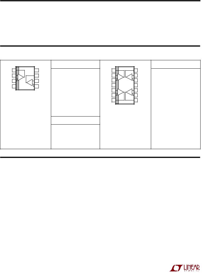
PACKAGE/ORDER IUFORWATIOU
TOP VIEW
OUT A |
1 |
|
|
8 |
V+ |
–IN A |
2 |
A |
|
7 |
OUT B |
|
|
|
|
|
|
+IN A |
3 |
|
B |
6 |
–IN B |
|
|
|
|
|
|
V– |
4 |
|
|
5 |
+IN B |
N8 PACKAGE |
S8 PACKAGE |
8-LEAD PDIP |
8-LEAD PLASTIC SO |
TJMAX = 150°C, θJA = 130°C/W (N8) TJMAX = 150°C, θJA = 190°C/W (S8)
ORDER PART NUMBER
LT1881CN8
LT1881IN8
LT1881CS8
LT1881IS8
LT1881ACN8
LT1881AIN8
LT1881ACS8
LT1881AIS8
S8 PART MARKING
1881
1881I
1881A
1881AI
TOP VIEW
OUT A |
1 |
|
|
14 |
OUT D |
–IN A |
2 |
A |
D |
13 |
–IN D |
+IN A |
3 |
12 |
|
||
|
|
+IN D |
|||
V+ |
4 |
|
|
11 |
V– |
+IN B |
5 |
B |
C |
10 |
+IN C |
|
6 |
9 |
|
||
–IN B |
|
|
–IN C |
||
OUT B |
7 |
|
|
8 |
OUT C |
S PACKAGE
14-LEAD PLASTIC SO
TJMAX = 150°C, θJA = 150°C/W
ORDER PART NUMBER
LT1882CS
LT1882IS
Consult factory for parts specified with wider operating temperature ranges.
ELECTRICAL CHARACTERISTICS
The ● denotes the specifications which apply over the full operating temperature range, otherwise specifications are at TA = 25°C.
Single supply operation VS = 5V, 0V; VCM = VS/2 unless otherwise noted. (Note 5)
SYMBOL |
PARAMETER |
|
CONDITIONS |
|
MIN |
TYP |
MAX |
UNITS |
|
VOS |
|
Input Offset Voltage |
(LT1881A) |
|
|
|
25 |
50 |
µV |
|
|
|
|
0°C < TA < 70°C |
● |
|
|
85 |
µV |
|
|
|
|
– 40°C < TA < 85°C |
● |
|
|
110 |
µV |
|
|
Input Offset Voltage (LT1881/LT1882) |
0°C < TA < 70°C |
|
|
30 |
80 |
µV |
|
|
|
|
|
● |
|
|
125 |
µV |
|
|
|
|
|
– 40°C < TA < 85°C |
● |
|
|
150 |
µV |
VOS/ |
T |
Input Offset Voltage Drift |
0°C < TA < 70°C |
● |
|
0.3 |
0.8 |
µV/°C |
|
|
|
(Note 6) |
|
– 40°C < TA < 85°C |
● |
|
0.3 |
0.8 |
µV/°C |
VOS/ |
TIME |
Long-Term Input Offset Voltage Stability |
|
|
|
0.3 |
|
µV/month |
|
IOS |
|
Input Offset Current |
(LT1881A) |
0°C < TA < 70°C |
|
|
100 |
200 |
pA |
|
|
|
|
● |
|
|
250 |
pA |
|
|
|
|
|
– 40°C < TA < 85°C |
● |
|
|
300 |
pA |
|
|
Input Offset Current (LT1881/LT1882) |
0°C < TA < 70°C |
|
|
150 |
500 |
pA |
|
|
|
|
|
● |
|
|
600 |
pA |
|
|
|
|
|
– 40°C < TA < 85°C |
● |
|
|
700 |
pA |
|
|
|
|
|
|
|
|
|
|
|
|
|
|
|
|
|
|
|
|
2

LT1881/LT1882
ELECTRICAL CHARACTERISTICS
The ● denotes the specifications which apply over the full operating temperature range, otherwise specifications are at TA = 25°C.
Single supply operation VS = 5V, 0V; VCM = VS/2 unless otherwise noted. (Note 5)
SYMBOL |
PARAMETER |
CONDITIONS |
|
MIN |
TYP |
MAX |
UNITS |
|
|||
|
|
|
|
|
|
|
|
|
|
|
|
IB |
Input Bias Current (LT1881A) |
0°C < TA < 70°C |
|
|
100 |
200 |
|
pA |
|||
|
|
● |
|
|
250 |
|
pA |
||||
|
|
– 40°C < TA < 85°C |
● |
|
|
300 |
|
pA |
|
||
|
Input Bias Current (LT1881/LT1882) |
0°C < TA < 70°C |
|
|
150 |
500 |
|
pA |
|||
|
|
● |
|
|
600 |
|
pA |
||||
|
|
– 40°C < TA < 85°C |
● |
|
|
700 |
|
pA |
|
||
|
Input Noise Voltage |
0.1Hz to 10Hz |
|
|
0.5 |
|
µVP-P |
|
|||
en |
Input Noise Voltage Density |
f = 1kHz |
|
|
14 |
|
nV/√ |
|
|
||
|
|
|
Hz |
||||||||
in |
Input Noise Current Density |
f = 1kHz |
|
|
0.03 |
|
pA/√ |
|
|
||
|
|
|
Hz |
||||||||
RIN |
Input Resistance |
Differential Mode |
● |
|
20 |
|
MΩ |
||||
|
|
Common Mode |
● |
|
100 |
|
GΩ |
|
|||
CIN |
Input Capacitance |
|
● |
|
2 |
|
|
|
pF |
||
VCM |
Input Voltage Range |
|
|
V– + 1.0 |
|
V+ – 1.0 |
|
|
V |
|
|
|
|
|
● |
V– + 1.2 |
|
V+ – 1.2 |
|
|
V |
|
|
CMRR |
Common Mode Rejection Ratio |
1V < VCM < 4V |
|
106 |
128 |
|
|
dB |
|||
|
|
1.2V < VCM < 3.8V |
● |
104 |
|
|
|
dB |
|||
PSRR |
Power Supply Rejection Ratio |
V– = 0V, V = 1.5V |
|
|
|
|
|
|
|
|
|
|
|
CM |
|
|
|
|
|
|
|
|
|
|
|
0°C < TA < 85°C, 2.7V < V+ < 32V |
● |
106 |
132 |
|
|
dB |
|||
|
|
TA = –40°C, 3V < V+ < 32V |
|
106 |
132 |
|
|
dB |
|
||
|
Minimum Operating Supply Voltage |
|
● |
|
2.4 |
2.7 |
|
|
V |
||
|
|
|
|
|
|
|
|
|
|
|
|
AVOL |
Large-Signal Voltage Gain |
RL = 10k; 1V < VOUT < 4V |
|
500 |
1600 |
|
V/mV |
||||
|
|
|
● |
350 |
|
|
V/mV |
|
|||
|
|
RL = 2k; 1V < VOUT < 4V |
|
300 |
800 |
|
V/mV |
||||
|
|
|
● |
250 |
|
|
V/mV |
|
|||
|
|
RL = 1k; 1V < VOUT < 4V |
|
250 |
400 |
|
V/mV |
||||
|
|
|
● |
200 |
|
|
V/mV |
|
|||
VOL |
Output Voltage Swing Low |
No Load |
● |
|
20 |
40 |
mV |
||||
|
|
ISINK = 100µA |
● |
|
25 |
50 |
mV |
||||
|
|
ISINK = 1mA |
● |
|
70 |
150 |
mV |
||||
|
|
ISINK = 5mA |
● |
|
270 |
600 |
mV |
|
|||
VOH |
Output Voltage Swing High |
No Load |
● |
|
120 |
220 |
mV |
||||
|
(Referred to V+) |
ISOURCE = 100µA |
● |
|
130 |
230 |
mV |
||||
|
|
ISOURCE = 1mA |
● |
|
180 |
300 |
mV |
||||
|
|
ISOURCE = 5mA |
● |
|
360 |
600 |
mV |
|
|||
IS |
Supply Current Per Amplifier |
VS = 3V, 0V |
|
0.45 |
0.65 |
0.85 |
mA |
||||
|
|
|
● |
|
|
1.2 |
mA |
|
|||
|
|
VS = 5V, 0V |
|
0.5 |
0.65 |
0.9 |
mA |
||||
|
|
|
● |
|
|
1.4 |
mA |
|
|||
|
|
VS = 12V, 0V |
|
0.5 |
0.70 |
1.0 |
mA |
||||
|
|
|
● |
|
|
1.5 |
mA |
|
|||
ISC |
Short-Circuit Current |
VOUT Short to GND |
● |
15 |
30 |
|
mA |
||||
|
|
VOUT Short to V+ |
● |
15 |
30 |
|
mA |
|
|||
GBW |
Gain Bandwidth Product |
f = 20kHz |
|
0.35 |
1.0 |
|
MHz |
||||
|
|
|
|
|
|
|
|
|
|
|
|
|
Channel Separation |
f = 1kHz |
|
|
120 |
|
|
dB |
|||
|
|
|
|
|
|
|
|
|
|
|
|
tS |
Settling Time |
0.01%, VOUT = 1.5V to 3.5V, |
|
|
30 |
|
|
|
µs |
||
|
|
AV = –1, RL = 2k |
|
|
|
|
|
|
|
|
|
|
|
|
|
|
|
|
|
|
|
|
|
|
|
|
|
|
|
|
|
|
|
|
|
|
|
|
|
|
|
|
3 |
|
|
||
|
|
|
|
|
|
|
|||||
|
|
|
|
|
|
|
|||||

LT1881/LT1882
ELECTRICAL CHARACTERISTICS
The ● denotes the specifications which apply over the full operating temperature range, otherwise specifications are at TA = 25°C.
Single supply operation VS = 5V, 0V; VCM = VS/2 unless otherwise noted. (Note 5)
SYMBOL |
PARAMETER |
CONDITIONS |
|
MIN |
TYP |
MAX |
UNITS |
|
|
|
|
|
|
|
|
SR + |
Slew Rate Positive |
AV = – 1 |
|
0.15 |
0.35 |
|
V/µs |
|
|
|
● |
0.12 |
|
|
V/µs |
SR – |
Slew Rate Negative |
AV = – 1 |
|
0.11 |
0.18 |
|
V/µs |
|
|
|
● |
0.08 |
|
|
V/µs |
FPBW |
Full-Power Bandwidth |
VOUT = 4VP-P |
|
8.75 |
14 |
|
kHz |
|
|
(Note 10) |
● |
6.35 |
|
|
kHz |
VOS |
Offset Voltage Match (LT1881A) |
(Note 7) |
|
|
30 |
70 |
µV |
|
|
0°C < TA < 70°C |
● |
|
|
125 |
µV |
|
|
– 40°C < TA < 85°C |
● |
|
|
160 |
µV |
|
Offset Voltage Match (LT1881/LT1882) |
(Note 7) |
|
|
35 |
125 |
µV |
|
|
0°C < TA < 70°C |
● |
|
|
175 |
µV |
|
|
– 40°C < TA < 85°C |
● |
|
|
235 |
µV |
|
Offset Voltage Match Drift |
(Notes 6, 7) |
● |
|
0.4 |
1.2 |
µV/°C |
IB+ |
Noninverting Bias Current Match |
(Notes 7, 8) |
|
|
200 |
300 |
pA |
|
(LT1881A) |
0°C < TA < 70°C |
● |
|
|
400 |
pA |
|
|
– 40°C < TA < 85°C |
● |
|
|
500 |
pA |
|
Noninverting Bias Current Match |
(Notes 7, 8) |
|
|
250 |
700 |
pA |
|
(LT1881/LT1882) |
0°C < TA < 70°C |
● |
|
|
900 |
pA |
|
|
– 40°C < TA < 85°C |
● |
|
|
1000 |
pA |
CMRR |
Common Mode Rejection Match |
(Notes 7, 9) |
● |
102 |
125 |
|
dB |
|
|
|
|
|
|
|
|
PSRR |
Power Supply Rejection Match |
V– = 0V, V = 1.5V |
|
|
|
|
|
|
|
CM |
|
|
|
|
|
|
(Notes 7, 9) |
0°C < TA < 85°C, 2.7V < V+ < 32V |
● |
104 |
126 |
|
dB |
|
|
TA = –40°C, 3V < V+ < 32V |
|
104 |
126 |
|
dB |
The ● denotes the specifications which apply over the full operating temperature range, otherwise specifications are at TA = 25°C. Split supply operation VS = ±15V, VCM = 0V unless otherwise noted. (Note 5)
SYMBOL |
PARAMETER |
CONDITIONS |
|
MIN |
TYP |
MAX |
UNITS |
|
|
|
|
|
|
|
|
|
|
VOS |
|
Input Offset Voltage (LT1881A) |
|
|
|
25 |
50 |
µV |
|
|
|
0°C < TA < 70°C |
● |
|
|
85 |
µV |
|
|
|
– 40°C < TA < 85°C |
● |
|
|
110 |
µV |
|
|
Input Offset Voltage (LT1881/LT1882) |
0°C < TA < 70°C |
|
|
30 |
80 |
µV |
|
|
|
● |
|
|
125 |
µV |
|
|
|
|
– 40°C < TA < 85°C |
● |
|
|
150 |
µV |
VOS/ |
T |
Input Offset Voltage Drift |
0°C < TA < 70°C |
● |
|
0.3 |
0.8 |
µV/°C |
|
|
(Note 6) |
– 40°C < TA < 85°C |
● |
|
0.3 |
0.8 |
µV/°C |
VOS/ |
TIME |
Long-Term Input Offset Voltage Stability |
|
|
|
0.3 |
|
µV/month |
IOS |
|
Input Offset Current (LT1881A) |
0°C < TA < 70°C |
|
|
150 |
200 |
pA |
|
|
|
● |
|
|
250 |
pA |
|
|
|
|
– 40°C < TA < 85°C |
● |
|
|
300 |
pA |
|
|
Input Offset Current (LT1881/LT1882) |
0°C < TA < 70°C |
|
|
150 |
500 |
pA |
|
|
|
● |
|
|
600 |
pA |
|
|
|
|
– 40°C < TA < 85°C |
● |
|
|
700 |
pA |
4

LT1881/LT1882
ELECTRICAL CHARACTERISTICS
The ● denotes the specifications which apply over the full operating temperature range, otherwise specifications are at TA = 25°C. Split supply operation VS = ±15V, VCM = 0V unless otherwise noted. (Note 5)
SYMBOL |
PARAMETER |
CONDITIONS |
|
MIN |
TYP |
MAX |
UNITS |
||
|
|
|
|
|
|
|
|
|
|
IB |
Input Bias Current (LT1881A) |
0°C < TA < 70°C |
|
|
150 |
200 |
pA |
||
|
|
● |
|
|
250 |
pA |
|||
|
|
– 40°C < TA < 85°C |
● |
|
|
300 |
pA |
||
|
Input Bias Current (LT1881/LT1882) |
0°C < TA < 70°C |
|
|
150 |
500 |
pA |
||
|
|
● |
|
|
600 |
pA |
|||
|
|
– 40°C < TA < 85°C |
● |
|
|
700 |
pA |
||
|
Input Noise Voltage |
0.1Hz to 10Hz |
|
|
0.5 |
|
µVP-P |
||
en |
Input Noise Voltage Density |
f = 1kHz |
|
|
14 |
|
nV/√ |
|
|
|
|
|
Hz |
||||||
in |
Input Noise Current Density |
f = 1kHz |
|
|
0.03 |
|
pA/√ |
|
|
|
|
|
Hz |
||||||
RIN |
Input Resistance |
Differential Mode |
● |
|
20 |
|
MΩ |
||
|
|
Common Mode |
● |
|
100 |
|
GΩ |
||
CIN |
Input Capacitance |
|
● |
|
2 |
|
|
pF |
|
VCM |
Input Voltage Range |
|
|
V– + 1.0 |
|
V+ – 1.0 |
|
V |
|
|
|
|
● |
V– + 1.2 |
|
V+ – 1.2 |
|
V |
|
CMRR |
Common Mode Rejection Ratio |
–13.5V < VCM < 13.5V |
● |
114 |
130 |
|
dB |
||
+PSRR |
Positive Power Supply Rejection Ratio |
V– = –15V, VCM = 0V; 1.5V < V+ < 18V |
● |
110 |
132 |
|
dB |
||
–PSRR |
Negative Power Supply Rejection Ratio |
V+ = 15V, V = 0V; –1.5V < V– < –18V |
● |
106 |
132 |
|
dB |
||
|
|
CM |
|
|
|
|
|
|
|
|
Minimum Operating Supply Voltage |
|
● |
|
±1.2 |
±1.35 |
|
V |
|
AVOL |
Large-Signal Voltage Gain |
RL = 10k; –13.5V < VOUT < 13.5V |
|
1000 |
1600 |
|
V/mV |
||
|
|
|
● |
700 |
|
|
V/mV |
||
|
|
RL = 2k; –13.5V < VOUT < 13.5V |
|
175 |
420 |
|
V/mV |
||
|
|
|
● |
125 |
|
|
V/mV |
||
|
|
RL = 1k; –12V < VOUT < 12V |
|
90 |
230 |
|
V/mV |
||
|
|
|
● |
65 |
|
|
V/mV |
||
VOL |
Output Voltage Swing Low |
No Load |
● |
|
20 |
40 |
mV |
||
|
(Referred to VEE) |
ISINK = 100µA |
● |
|
25 |
50 |
mV |
||
|
|
ISINK = 1mA |
● |
|
70 |
150 |
mV |
||
|
|
ISINK = 5mA |
● |
|
270 |
600 |
mV |
||
VOH |
Output Voltage Swing High |
No Load |
● |
|
160 |
220 |
mV |
||
|
(Referred to VCC) |
ISOURCE = 100µA |
● |
|
160 |
230 |
mV |
||
|
|
ISOURCE = 1mA |
● |
|
180 |
300 |
mV |
||
|
|
ISOURCE = 5mA |
● |
|
360 |
600 |
mV |
||
IS |
Supply Current Per Amplifier |
VS = ±15V |
|
0.5 |
0.85 |
1.1 |
mA |
||
|
|
|
● |
|
|
1.6 |
mA |
||
ISC |
Short-Circuit Current |
VOUT Short to V– |
|
20 |
40 |
|
mA |
||
|
|
|
● |
15 |
40 |
|
mA |
||
|
|
VOUT Short to V+ |
|
20 |
30 |
|
mA |
||
|
|
|
● |
15 |
30 |
|
mA |
||
GBW |
Gain Bandwidth Product |
f = 20kHz |
|
0.4 |
0.85 |
|
MHz |
||
|
|
|
|
|
|
|
|
|
|
|
Channel Separation |
f = 1kHz |
|
|
120 |
|
dB |
||
|
|
|
|
|
|
|
|
|
|
tS |
Settling Time |
0.01%, VOUT = – 5V to 5V, |
|
|
35 |
|
|
µs |
|
|
|
AV = –1, RL = 2k |
|
|
|
|
|
|
|
SR + |
Slew Rate Positive |
AV = – 1 |
|
0.21 |
0.4 |
|
V/µs |
||
|
|
|
● |
0.18 |
|
|
V/µs |
||
5

LT1881/LT1882
ELECTRICAL CHARACTERISTICS
The ● denotes the specifications which apply over the full operating temperature range, otherwise specifications are at TA = 25°C. Split supply operation VS = ±15V, VCM = 0V unless otherwise noted. (Note 5)
SYMBOL |
PARAMETER |
CONDITIONS |
|
MIN |
TYP |
MAX |
UNITS |
SR – |
Slew Rate Negative |
AV = – 1 |
|
0.13 |
0.20 |
|
V/µs |
|
|
|
● |
0.1 |
|
|
V/µs |
FPBW |
Full-Power Bandwidth |
VOUT = 28VP-P |
|
1.47 |
2.25 |
|
kHz |
|
|
(Note 10) |
● |
1.13 |
|
|
kHz |
VOS |
Offset Voltage Match (LT1881/LT1882) |
(Note 5) |
|
|
42 |
125 |
µV |
|
|
0°C < TA < 70°C |
● |
|
|
175 |
µV |
|
|
– 40°C < TA < 85°C |
● |
|
|
235 |
µV |
|
Offset Voltage Match (LT1881A) |
|
|
|
35 |
70 |
µV |
|
|
0°C < TA < 70°C |
● |
|
|
125 |
µV |
|
|
– 40°C < TA < 85°C |
● |
|
|
160 |
µV |
|
Offset Voltage Match Drift |
(Notes 6, 7) |
● |
|
0.4 |
1.1 |
µV/°C |
IB+ |
Noninverting Bias Current Match |
(Notes 7, 8) |
|
|
240 |
700 |
pA |
|
(LT1881/LT1882) |
0°C < TA < 70°C |
● |
|
|
900 |
pA |
|
|
– 40°C < TA < 85°C |
● |
|
|
1000 |
pA |
|
Noninverting Bias Current Match |
0°C < TA < 70°C |
|
|
200 |
300 |
pA |
|
(LT1881A) |
● |
|
|
400 |
pA |
|
|
|
– 40°C < TA < 85°C |
● |
|
|
500 |
pA |
CMRR |
Common Mode Rejection Match |
(Notes 7, 9) |
● |
110 |
125 |
|
dB |
|
|
|
|
|
|
|
|
+PSRR |
Positive Power Supply Rejection Match |
V– = – 15V, VCM = 0V, |
● |
108 |
130 |
|
dB |
|
|
1.5V < V+ < 18V, (Notes 7, 9) |
|
|
|
|
|
–PSRR |
Negative Power Supply Rejection Match |
V+ = 15V, V = 0V, |
● |
104 |
130 |
|
dB |
|
|
CM |
|
|
|
|
|
|
|
– 1.5V < V– < – 18V, (Notes 7, 9) |
|
|
|
|
|
Note 1: Absolute Maximum Ratings are those values beyond which the life of a device may be impaired.
Note 2: The inputs are protected by internal resistors and back-to-back diodes. If the differential input voltage exceeds ±0.7V, the input current should be limited externally to less than 10mA.
Note 3: A heat sink may be required to keep the junction temperature below absolute maximum.
Note 4: The LT1881C, LT1882C, LT1881I and LT1882I are guaranteed functional over the operating temperature range of – 40°C to 85°C. Note 5: The LT1881C and LT1882C are designed, characterized and expected to meet specified performance from – 40°C to 85°C but are not
tested or QA sampled at these temperatures. The LT1881I and LT1882I are guaranteed to meet specified performance from – 40°C to 85°C.
Note 6: This parameter is not 100% tested.
Note 7: Matching parameters are the difference between amplifiers
A and B in the LT1881; and between amplifiers A and D and B and C in the LT1882.
Note 8: This parameter is the difference between the two noninverting input bias currents.
Note 9: CMRR and PSRR are defined as follows: CMRR and PSRR are measured in µV/V on each amplifier. The difference is calculated in µV/V and then converted to dB.
Note 10: Full power bandwidth is calculated from the slew rate: FPBW = SR/2πVP.
6
|
|
LT1881/LT1882 |
|
|
|
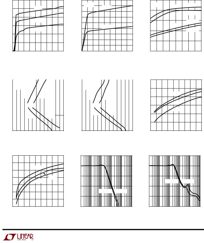
TYPICAL PERFORWAUCE CHARACTERISTICS |
|
|
Supply Current per Amplifier vs |
|
|
Supply Voltage |
Slew Rate vs Supply Voltage |
Slew Rate vs Temperature |
|
1200 |
|
|
|
|
|
|
|
|
|
|
0.45 |
|
|
|
|
|
|
|
|
|
0.5 |
|
|
|
|
|
|
|
|
|
|
|
( A) |
|
|
|
|
125°C |
|
|
|
|
|
0.40 |
AV = –1 |
|
RISING |
|
|
|
|
|
AV = –1 |
|
|
RISING |
|
V |
S |
= ±15V |
|
|||||
1000 |
|
|
|
|
|
|
|
|
|
|
|
|
|
|
|
|
|
|
|
|
|
|
|
|
|
||||||||
|
|
|
|
|
|
|
|
|
|
|
|
|
|
|
|
|
|
|
|
|
|
|
|
|
|
|
|||||||
CURRENT PER AMPLIFIER |
|
|
|
|
|
|
|
|
|
|
0.35 |
|
|
|
|
|
|
|
|
|
0.4 |
|
|
|
|
|
|
|
|
|
|
|
|
|
|
|
|
|
|
|
|
|
|
|
|
|
|
|
|
|
|
|
|
|
|
|
|
|
VS = |
±5V |
|
||||||
|
|
|
|
|
|
|
|
|
|
|
|
|
|
|
|
|
|
|
|
|
|
|
|
|
|
|
|||||||
800 |
|
|
|
25°C |
|
|
|
|
|
0.30 |
|
|
|
|
|
|
|
|
|
|
|
|
|
|
|
|
|
|
|
|
|
||
|
|
|
|
|
|
|
|
|
0.25 |
|
|
|
|
|
|
|
|
|
0.3 |
|
|
|
|
|
VS = |
±15V |
|
||||||
|
|
|
|
|
|
|
|
|
|
|
|
|
|
|
|
|
|
|
|
|
|
|
|
|
|
||||||||
600 |
|
|
|
|
|
|
|
|
|
|
|
|
|
|
|
|
|
|
|
|
|
|
|
FALLING |
|
||||||||
|
|
|
–55°C |
|
|
|
|
|
0.20 |
|
|
|
FALLING |
|
|
|
|
|
|
|
|
VS = |
± |
5V |
|
||||||||
|
|
|
|
|
|
|
|
|
|
|
|
|
|
|
|
|
|
0.2 |
|
|
|
|
|
|
|||||||||
|
|
|
|
|
|
|
|
|
|
|
|
|
|
|
|
|
|
|
|
|
|
|
|
|
|
|
|
||||||
400 |
|
|
|
|
|
|
|
|
|
RATESLEW(V/s) |
0.15 |
|
|
|
|
|
|
|
|
|
RATESLEW(V/s) |
|
|
|
|
|
|
|
|
|
|
|
|
|
|
|
|
|
|
|
|
|
|
|
|
|
|
|
|
|
|
|
|
|
|
|
|
|
|
|
|
|
|
|
|||
SUPPLY |
200 |
|
|
|
|
|
|
|
|
|
|
0.10 |
|
|
|
|
|
|
|
|
|
0.1 |
|
|
|
|
|
|
|
|
|
|
|
|
|
|
|
|
|
|
|
|
|
|
|
|
|
|
|
|
|
|
|
|
|
|
|
|
|
|
|
|
|
|
|||
|
|
|
|
|
|
|
|
|
|
0.05 |
|
|
|
|
|
|
|
|
|
|
|
|
|
|
|
|
|
|
|
|
|
||
|
|
|
|
|
|
|
|
|
|
|
|
|
|
|
|
|
|
|
|
|
|
|
|
|
|
|
|
|
|
|
|
||
|
0 |
4 |
8 |
12 |
16 |
20 |
24 |
28 |
32 |
36 |
|
0 |
4 |
8 |
12 |
16 |
20 |
24 |
28 |
32 |
36 |
0 |
–25 |
0 |
25 |
50 |
75 |
100 |
125 |
150 |
|||
|
0 |
|
0 |
–50 |
|||||||||||||||||||||||||||||
|
|
|
TOTAL SUPPLY VOLTAGE (V) |
|
|
|
|
|
TOTAL SUPPLY VOLTAGE (V) |
|
|
|
|
|
TEMPERATURE (°C) |
|
|
|
|
|
|||||||||||||
|
|
|
|
|
|
|
|
|
1881/2 G01 |
|
|
|
|
|
|
|
|
|
1881/2 G02 |
|
|
|
|
|
|
|
|
|
|
1881/2 G03 |
|||
OUTPUT STEP (V)
Settling Time vs Output Step
10 |
|
|
|
|
|
|
|
|
|
|
|
|
|
|
|
|
|
|
|
|
|
|
|
|
|
|
|
|
|
|
|
|
|
|
|
|
|
|
|
|
|
8 |
|
VS = ±15V |
|
|
|
|
|
|
|
|
|
|
|
|
|
|||||
|
|
|
|
|
|
|
|
|
|
|
|
|
|
|||||||
6 |
|
AV = –1 |
|
|
|
|
|
|
|
|
|
|
|
|
||||||
|
|
|
|
|
|
|
|
|
|
|
|
|
|
|
|
|
|
|
|
|
4 |
|
|
|
|
|
|
|
|
|
|
|
|
|
|
|
|
||||
|
|
|
|
0.1% |
|
|
|
0.01% |
|
|
|
|
||||||||
|
|
|
|
|
|
|
|
|
|
|||||||||||
2 |
|
|
|
|
|
|
|
|
|
|
|
|
|
|
|
|
|
|
|
|
|
|
|
|
|
|
|
|
|
|
|
|
|
|
|
|
|
|
|
|
|
|
|
|
|
|
|
|
|
|
|
|
|
|
|
|
|
|
|
|
|
|
0 |
|
|
|
|
|
|
|
|
|
|
|
|
|
|
|
|
|
|
|
|
|
|
|
|
|
|
|
|
|
|
|
|
|
|
|
|
|
|
|
|
|
–2 |
|
|
|
|
|
|
|
|
|
|
|
|
|
|
|
|
|
|
|
|
|
|
|
|
|
|
|
|
|
|
|
|
|
|
|
|
|
|
|
|
|
–4 |
|
|
|
|
|
|
|
|
|
|
|
|
|
|
|
|
||||
|
|
|
|
|
|
0.1% |
|
|
|
|
0.01% |
|
||||||||
|
|
|
|
|
|
|
|
|
||||||||||||
–6 |
|
|
|
|
|
|
|
|
|
|
|
|
|
|
|
|
|
|
|
|
|
|
|
|
|
|
|
|
|
|
|
|
|
|
|
|
|
|
|
|
|
|
|
|
|
|
|
|
|
|
|
|
|
|
|
|
|
|
|
|
|
|
–8 |
|
|
|
|
|
|
|
|
|
|
|
|
|
|
|
|
|
|
|
|
|
|
|
|
|
|
|
|
|
|
|
|
|
|
|
|
|
|
|
|
|
–10
0 5 10 15 20 25 30 35 40 45 50 55 60 65 SETTLING TIME ( s)
OUTPUT STEP (V)
Settling Time vs Output Step
10 |
|
|
|
|
|
|
|
|
|
|
|
|
|
|
|
|
|
|
|
|
|
|
|
|
|
|
|
|
|
|
|
|
|
|
|
8 |
|
VS = ±15V |
|
|
|
|
|
|
|
|
|
||||||
|
|
|
|
|
|
|
|
|
|
||||||||
6 |
|
AV = 1 |
|
|
|
|
|
|
|
|
|
||||||
|
|
|
|
|
|
|
|
|
|
|
|
|
|
|
|
|
|
4 |
|
|
|
|
|
|
|
|
|
|
|
|
|
|
|
|
|
|
|
|
0.1% |
|
|
|
0.01% |
|
|
|
|||||||
2 |
|
|
|
|
|
|
|
||||||||||
|
|
|
|
|
|
|
|
|
|
|
|
|
|
|
|
|
|
|
|
|
|
|
|
|
|
|
|
|
|
|
|
|
|
|
|
0 |
|
|
|
|
|
|
|
|
|
|
|
|
|
|
|
|
|
|
|
|
|
|
|
|
|
|
|
|
|
|
|
|
|
|
|
–2 |
|
|
|
|
|
|
|
|
|
|
|
|
|
|
|
|
|
|
|
|
|
|
0.1% |
|
|
|
0.01% |
|
|||||||
–4 |
|
|
|
|
|
||||||||||||
|
|
|
|
|
|
|
|
|
|
|
|
|
|
|
|
|
|
|
|
|
|
|
|
|
|
|
|
|
|
|
|
|
|
|
|
|
|
|
|
|
|
|
|
|
|
|
|
|
|
|
|
|
|
–6 |
|
|
|
|
|
|
|
|
|
|
|
|
|
|
|
|
|
|
|
|
|
|
|
|
|
|
|
|
|
|
|
|
|
|
|
–8 |
|
|
|
|
|
|
|
|
|
|
|
|
|
|
|
|
|
|
|
|
|
|
|
|
|
|
|
|
|
|
|
|
|
|
|
–10
0 5 10 15 20 25 30 35 40 45 50 55 60 65 SETTLING TIME ( s)
GAIN BANDWIDTH PRODUCT (kHz)
Gain Bandwidth Product vs
Supply Voltage
900
850
125°C
800
25°C
750
–55°C
700
650
600
0 |
4 |
8 |
12 |
16 |
20 |
24 |
28 |
32 |
36 |
|
|
TOTAL SUPPLY VOLTAGE (V) |
|
|
|||||
1881/2 G04 1881/2 G05 1881/2 G06
Phase Margin vs Supply Voltage Gain vs Frequency, AV = –1 Gain vs Frequency, AV = 1
|
60 |
|
|
|
|
|
|
|
|
|
|
10 |
|
|
|
|
|
|
58 |
|
|
|
|
|
|
|
|
|
|
0 |
|
|
|
|
|
|
|
|
|
|
–55°C |
|
|
|
|
|
|
|
|
|
|
||
(DEG) |
56 |
|
|
|
|
|
|
|
|
|
|
|
|
|
|
||
|
|
|
|
|
|
|
|
|
|
|
|
|
|
|
|
||
|
|
|
|
|
|
|
|
|
|
|
|
|
|
|
|
|
|
MARGINPHASE |
50 |
|
|
|
|
|
|
125°C |
|
|
(dB)GAIN |
–10 |
|
VS = ±2.5V |
VS = ±15V |
(dB)GAIN |
|
|
54 |
|
|
|
125°C |
|
|
|
|
|
|
|
|
|
|
||
|
|
|
|
|
|
|
|
|
|
|
|
|
|
|
|
||
|
52 |
|
|
|
|
|
|
|
|
|
|
–20 |
|
|
|
|
|
|
|
|
|
|
|
|
|
|
|
|
|
|
|
|
|
|
|
|
48 |
|
|
|
|
|
|
|
|
|
|
–30 |
|
|
|
|
|
|
|
|
|
|
|
|
|
|
|
|
|
|
|
|
|
|
|
|
46 |
4 |
8 |
12 |
16 |
20 |
24 |
28 |
32 |
36 |
|
–40 |
10k |
100k |
1M |
10M |
100M |
|
0 |
|
1k |
||||||||||||||
|
|
|
TOTAL SUPPLY VOLTAGE (V) |
|
|
|
|
|
FREQUENCY (Hz) |
|
|||||||
10
0
–10
VS = ±2.5V VS = ±15V
–20
–30
–40
1k |
10k |
100k |
1M |
10M |
100M |
FREQUENCY (Hz)
1881/2 G07 |
1881/2 G08 |
1881/2 G09 |
7

LT1881/LT1882
TYPICAL PERFORWAUCE CHARACTERISTICS
|
Gain vs Frequency with CLOAD, |
|
||||
|
AV = 1 |
|
|
|
|
|
|
10 |
|
|
|
|
|
|
|
VS = ±15V |
|
|
|
|
|
0 |
|
|
|
1500pF |
|
|
|
|
|
|
||
|
–10 |
|
|
|
1000pF |
|
(dB) |
|
|
|
500pF |
(dB) |
|
|
|
|
|
|||
GAIN |
–20 |
|
|
|
|
GAIN |
|
|
|
|
0pF |
|
|
|
|
|
|
|
|
|
|
–30 |
|
|
|
|
|
|
–40 |
10k |
100k |
1M |
10M |
100M |
|
1k |
|||||
|
|
|
FREQUENCY (Hz) |
|
|
|
|
|
|
|
|
1881/2 G10 |
|
Gain vs Frequency with CLOAD,
AV = –1
10 


 VS = ±15V
0
1800pF
–10
1000pF
–20
500pF
–30 

 0pF
0pF
–40
1k |
10k |
100k |
1M |
10M |
100M |
FREQUENCY (Hz)
1881/2 G11
Large Signal Response, AV = –1 |
Large Signal Response, AV = 1 |
Small Signal Response, AV = –1, |
|||
No Load |
|
||||
OUT |
|
OUT |
|
(20mV/DIV) |
|
(5V/DIV) |
|
(5V/DIV) |
|
|
|
V |
|
V |
|
OUT |
|
|
|
|
|
V |
|
TIME (50 s/DIV) |
1881/2 G12 |
|
1881/2 G13 |
|
1881/2 G14 |
|
|
TIME (50 s/DIV) |
TIME (2 s/DIV) |
||
Small Signal Response, AV = –1, |
Small Signal Response, AV = 1, |
Small Signal Response, AV = 1, |
|||
CL = 1000pF |
|
RL = 2k |
|
CL = 500pF |
|
(20mV/DIV) |
|
(20mV/DIV) |
|
(20mV/DIV) |
|
OUT |
|
OUT |
|
OUT |
|
V |
|
V |
|
V |
|
TIME (2 s/DIV) |
1881/2 G15 |
TIME (2 s/DIV) |
1881/2 G16 |
TIME (2 s/DIV) |
1881/2 G17 |
8
|
|
|
|
|
|
|
|
|
|
|
|
|
|
|
|
|
|
|
|
|
LT1881/LT1882 |
||||||
TYPICAL PERFORWAUCE CHARACTERISTICS |
|
|
|
|
|
|
|
|
|
||||||||||||||||||
|
|
LT1881 VOS Distribution, |
|
|
|
LT1881IS8 Voltage Offset vs |
|
|
|
|
|
|
|
|
|
|
|||||||||||
|
|
TA = 25°C |
|
|
|
|
|
|
Temperature |
|
|
|
|
|
|
Warm-Up Drift vs Time |
|
|
|
||||||||
|
26 |
VS = ±15V |
|
|
|
|
|
|
200 |
|
|
|
|
|
|
|
|
|
5 |
|
|
|
|
|
|
|
|
|
24 |
|
|
|
|
|
|
150 |
VS = ±15V |
|
|
|
|
|
|
|
0 |
|
|
|
|
|
|
|
|||
|
22 |
40 N8 (1 LOT) |
|
|
|
|
|
|
|
|
|
|
|
|
|
|
|
|
|
|
|
|
|
||||
|
|
|
|
|
|
|
|
|
|
|
|
|
|
|
|
|
|
N8 VS = 5V |
|
|
|
||||||
|
20 |
|
|
|
|
|
100 |
|
|
|
|
|
|
|
|
|
|
|
|
|
|
|
|||||
PERCENTOF UNITS (%) |
144 S8 (2 LOTS) |
|
|
|
|
VOLTAGEOFFSET ( V) |
|
|
|
|
|
|
|
|
|
–5 |
|
|
|
|
|
|
|
||||
6 |
|
|
|
|
|
|
|
–100 |
|
|
|
|
|
|
|
|
|
|
|
|
|
|
|
|
|||
|
|
|
|
|
|
|
|
|
|
|
|
|
|
|
|
VOLTAGEOFFSETDRIFTV)( |
|
|
|
|
|
|
|
||||
|
18 |
184 TOTAL PARTS |
|
|
|
|
|
50 |
|
|
|
|
|
|
|
|
|
|
|
|
|
|
|
|
|
||
|
16 |
|
|
|
|
|
|
|
|
|
|
|
|
|
|
|
|
|
–10 |
|
|
|
|
|
|
|
|
|
14 |
|
|
|
|
|
|
|
|
0 |
|
|
|
|
|
|
|
|
|
|
|
|
|
|
|
|
|
|
12 |
|
|
|
|
|
|
|
|
|
|
|
|
|
|
|
|
|
|
–15 |
|
|
|
|
|
|
|
|
10 |
|
|
|
|
|
|
|
|
–50 |
|
|
|
|
|
|
|
|
|
|
|
|
|
|
|
|
|
|
|
|
|
|
|
|
|
|
|
|
|
|
|
|
|
|
|
|
N8 VS = ±15V |
S8 VS = 5V, ±15V |
|
||||||
|
8 |
|
|
|
|
|
|
|
|
|
|
|
|
|
|
|
|
|
|
|
|
||||||
|
|
|
|
|
|
|
|
|
|
|
|
|
|
|
|
|
|
|
–20 |
|
|
|
|
|
|
|
|
|
|
|
|
|
|
|
|
|
|
|
|
|
|
|
|
|
|
|
|
|
|
|
|
|
|
|
|
|
4 |
|
|
|
|
|
|
|
|
–150 |
|
|
|
|
|
|
|
|
|
–25 |
|
|
|
|
|
|
|
|
2 |
|
|
|
|
|
|
|
|
|
|
|
|
|
|
|
|
|
|
|
|
|
|
|
|
|
|
|
0 |
–60 |
–40 |
–20 |
0 |
20 |
40 |
60 |
|
–200 |
–35 |
–15 |
5 |
25 |
45 |
65 |
85 |
105 |
125 |
–30 |
20 |
40 |
60 |
80 |
100 |
120 |
140 |
|
|
|
–55 |
0 |
|||||||||||||||||||||||
|
|
|
OUTPUT OFFSET VOLTAGE (µV) |
|
|
|
|
|
TEMPERATURE (°C) |
|
|
|
|
|
TIME AFTER POWER UP (s) |
|
|
||||||||||
|
|
|
|
|
|
|
1881/2 G18 |
|
|
|
|
|
|
|
|
|
1881/2 G19 |
|
|
|
|
|
|
1881/2 G20 |
|||
LT1881 Input Bias Current vs
Common Mode Voltage
|
1000 |
|
|
|
|
|
|
|
|
|
|
|
|
|
|
|
|
|
|
|
|
|
|
|
800 |
|
VS = ±15V |
|
|
|
|
|
|
||
|
|
|
|
|
|
|
|
||||
|
600 |
|
|
|
|
|
|
|
|
|
|
|
|
|
|
|
|
|
|
|
|
|
|
|
400 |
|
|
|
|
|
|
|
|
|
|
|
|
|
|
|
|
|
|
|
|
|
|
(pA) |
200 |
|
|
|
|
|
|
|
|
|
|
|
|
|
|
|
|
|
|
|
|
||
0 |
|
|
|
|
|
|
|
|
|
|
|
BIAS |
|
|
|
|
|
|
|
|
|
|
|
|
|
|
|
|
|
|
|
|
|
||
200 |
|
|
|
|
|
|
|
|
|
|
|
I |
|
|
|
|
|
|
|
|
|
|
|
|
400 |
|
|
|
|
|
|
|
|
|
|
|
|
|
|
|
|
|
|
|
|
|
|
|
600 |
|
|
|
|
|
|
|
|
|
|
|
|
|
|
|
|
|
|
|
|
|
|
|
800 |
|
|
|
|
|
|
|
|
|
|
|
|
|
|
|
|
|
|
|
|
|
|
|
1000 |
|
|
|
|
|
|
|
|
|
|
|
|
|
|
|
|
|
|
|
|
|
|
–20 –15 –10 –5 0 5 10 15 20 VCM (V)
1881/2 G21
LT1881 Input Bias Current vs |
LT1881 Input Common Mode |
Temperature |
Range vs Supply Voltage |
150 |
|
|
|
|
|
|
|
V+ – 0 |
|
|
|
|
|
|
|
|
|
|
VS = ±15V |
|
|
|
|
(V) |
V |
+ |
– 0.5 |
VOS < 1mV |
|
|
85°C |
|
|
||
100 |
|
|
|
|
|
|
|
|
|
|
|
|
|
|
|||
|
|
|
|
|
|
|
|
|
|
|
|
|
|
|
|
||
CURRENTBIASINPUT (pA) |
|
|
|
|
|
COMMONINPUTMODE RANGE |
V |
– |
+ 0.5 |
|
|
|
|
|
|
|
|
50 |
|
|
+IBIAS |
|
|
|
V+ |
– 1.0 |
|
|
|
|
|
|
|
|
|
|
|
|
|
|
|
|
V+ – 1.5 |
|
|
–40°C |
25°C |
|
|
|
|||
0 |
|
|
|
|
|
|
|
|
|
|
|
|
|
|
|
|
|
|
|
|
–IBIAS |
|
|
|
V |
– + 1.5 |
|
|
–40°C |
25°C |
|
|
|
||
–50 |
|
|
|
|
|
|
|
|
|
|
|
||||||
|
|
|
|
|
|
|
|
|
|
|
|
|
|
|
|
|
|
|
|
|
|
|
|
|
V – + 1.0 |
|
|
|
|
|
|
|
|
||
–100 |
|
|
|
|
|
|
|
|
|
|
|
|
|
|
|
|
|
|
|
|
|
|
|
|
|
V – + 0 |
|
|
|
|
85°C |
|
|
||
–150 |
–20 |
0 |
20 |
40 |
60 |
80 |
|
2 |
4 |
6 |
8 |
10 |
12 |
14 |
16 |
||
–40 |
|
|
0 |
||||||||||||||
|
|
TEMPERATURE (°C) |
|
|
|
|
|
|
SUPPLY VOLTAGE (±V) |
|
|
||||||
|
|
|
|
|
|
1881/2 G22 |
|
|
|
|
|
|
|
|
|
1881/2 G23 |
|
INPUT COMMON MODE VOLTAGE (V)
LT1881 Input Common Mode |
LT1881 Output Voltage Swing vs |
LT1881 Output Saturation Voltage |
Voltage vs Temperature |
Supply Voltage |
vs Load Current (Output High) |
5 |
|
|
|
|
|
|
|
|
V+ – 0 |
|
|
|
|
|
|
RL = 10k |
|
|
|
1 |
|
|
|
|
||
4 |
|
|
|
|
|
|
|
|
|
|
|
|
|
|
|
|
|
|
VOLTAGE(V) |
|
VS = ±15V |
|
|
|
||
3 |
|
|
|
|
|
|
SWING(V) |
V |
+ |
– 0.5 |
|
|
|
|
|
|
|
|
|
|
|
VOD = 30mV |
TA = 85°C |
|||
|
|
|
|
|
|
|
|
|
|
|
|
|
RL = 2k |
|
|
|
|
|
||||||||
|
|
|
|
|
|
|
|
|
|
|
|
|
|
|
|
|
|
|
|
|
|
|
||||
|
|
|
|
|
|
|
|
|
|
|
|
|
|
|
|
|
|
|
|
|
|
|
|
|
||
2 |
|
|
|
|
|
|
|
V+ – 1.0 |
|
|
|
|
|
|
|
|
|
|
|
|
|
TA = 25°C |
|
|
||
|
|
|
|
|
|
|
|
|
|
|
|
|
|
|
|
|
|
|
|
|
|
|
||||
1 |
|
|
|
|
|
|
VOLTAGEOUTPUT |
|
|
|
AV = –1 |
|
|
|
|
|
|
|
SATURATIONOUTPUT |
|
|
|
|
|
||
0 |
VS = ±5V |
|
|
|
|
|
|
|
|
|
|
|
|
|
|
|
0.1 |
|
|
|
|
|||||
|
|
|
|
|
|
|
|
|
TA = 25°C |
|
|
|
|
|
|
|
|
|
|
TA = –40°C |
||||||
–1 |
|
|
|
|
|
|
|
|
|
|
|
|
|
|
|
|
|
|
|
|
|
|||||
|
|
|
|
|
|
|
V – + 1.0 |
|
|
|
|
|
|
|
|
|
|
|
|
|
|
|
|
|||
–2 |
|
|
|
|
|
|
|
|
|
|
|
|
|
|
|
|
|
|
|
|
|
|
|
|||
|
|
|
|
|
|
|
|
|
|
|
|
|
|
|
|
RL = 2k |
|
|
|
|
|
|
|
|
||
–3 |
|
|
|
|
|
|
|
V – + 0.5 |
|
|
|
|
|
|
|
|
|
|
|
|
|
|
||||
|
|
|
|
|
|
|
|
|
|
|
|
|
|
|
|
|
|
|
|
|
|
|
||||
–4 |
|
|
|
|
|
|
|
|
|
|
|
|
|
|
|
|
RL = 10k |
|
|
|
|
|
|
|
|
|
–5 |
–25 |
0 |
25 |
50 |
75 |
100 |
125 |
|
V – + 0 |
2 |
4 |
6 |
8 |
10 |
12 |
14 |
16 |
18 |
20 |
|
0.01 |
0.01 |
0.1 |
1 |
10 |
|
–50 |
|
|
0 |
|
0.001 |
|||||||||||||||||||||
|
|
TEMPERATURE (°C) |
|
|
|
|
|
|
|
SUPPLY VOLTAGE (±V) |
|
|
|
|
|
SOURCING LOAD CURRENT (mA) |
|
|||||||||
|
|
|
|
|
|
1881/2 G24 |
|
|
|
|
|
|
|
|
|
|
1881/2 G25 |
|
|
|
|
|
|
1881/2 G26 |
||
|
|
|
|
|
|
|
|
|
|
|
|
|
|
|
|
|
|
|
|
|
|
|
|
|
|
9 |
LT1881/LT1882
TYPICAL PERFORWAUCE CHARACTERISTICS
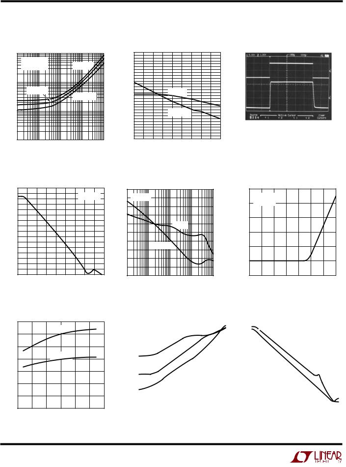
LT1881 Output Saturation Voltage vs Load Current (Output Low)
|
1 |
|
|
(V) |
VS = ±15V |
TA = 85°C |
|
VOD = 30mV |
|||
VOLTAGE |
0.1 |
|
|
TA = 25°C |
|
||
SATURATION |
TA = –40°C |
||
|
|||
0.01 |
|
||
OUTPUT |
|
|
|
0.001 |
|
||
0.001 0.01 0.1 1 10 SINKING LOAD CURRENT (mA)
1881/2 G27
LT1881 Output Short-Circuit |
LT1881 Output Voltage vs Large |
Current vs Temperature |
Input Voltage |
|
60 |
|
|
|
|
|
|
|
|
(mA) |
56 |
|
|
|
|
|
|
|
|
52 |
|
|
|
|
|
|
|
|
|
CURRENT |
48 |
|
|
|
|
|
|
VIN |
GND |
|
44 |
|
|
|
|
|
|
|
|
|
40 |
|
|
|
|
|
|
|
|
CIRCUIT |
36 |
|
SINKING |
|
|
|
VOUT |
GND |
|
28 |
|
|
|
|
|||||
|
32 |
|
|
|
|
|
|
||
- |
24 |
|
|
|
|
|
|
|
|
SHORT |
|
|
|
|
|
|
|
|
|
20 |
|
SOURCING |
|
|
|
|
|||
|
|
|
|
|
|
||||
|
16 |
|
|
|
|
|
|||
OUTPUT |
|
|
|
|
|
|
VS = ±2.5V |
|
|
12 |
|
|
|
|
|
|
|
||
|
|
|
|
|
|
|
AV = 1 |
1881 G29.tif |
|
|
8 |
|
|
|
|
|
|
||
|
|
|
|
|
|
|
|
|
|
|
4 |
|
|
|
|
|
|
VIN = ±5V |
|
|
0 |
|
|
|
|
|
|
|
|
|
– 55 –35 –15 |
5 |
25 |
45 |
65 |
85 |
105 125 |
RIN = 10k |
|
|
|
TEMPERATURE (°C) |
|
|
|
|
|||
|
|
|
|
|
|
|
1881/2 G28 |
|
|
LOOP GAIN (dB)
LT1881 Open-Loop Gain vs |
LT1881 Open-Loop Gain and |
LT1881 Channel Separation vs |
Frequency |
Phase vs Frequency |
Frequency |
140 |
|
|
|
|
|
|
|
70 |
|
|
|
175 |
|
|
–20 |
|
|
|
|
|
|
|
130 |
|
|
|
|
VS = |
±15V |
|
60 |
VS = ±5V |
|
|
150 |
|
|
|
VS = ±15V |
|
|
|
|
|
|
120 |
|
|
|
|
|
|
|
|
|
|
|
|
|
|
|
|||||||
|
|
|
|
|
|
|
|
|
|
|
|
|
|
–40 |
AV = 10 |
|
|
|
|
|
|
|
110 |
|
|
|
|
|
|
|
50 |
|
|
|
120 |
|
(dB) |
|
|
|
|
|
|
||
100 |
|
|
|
|
|
|
|
|
|
|
|
|
|
|
|
|
|
|
|
|||
|
|
|
|
|
|
|
40 |
|
|
|
100 |
|
|
|
|
|
|
|
|
|
||
90 |
|
|
|
|
|
|
LOOPGAIN (dB) |
|
|
|
(DEG)PHASE |
SEPARATIONCHANNEL |
–60 |
|
|
|
|
|
|
|
||
20 |
|
|
|
|
|
|
|
|
|
|
|
|
|
|
|
|
|
|
||||
80 |
|
|
|
|
|
|
|
30 |
|
PHASE |
|
75 |
|
|
|
|
|
|
|
|
|
|
70 |
|
|
|
|
|
|
|
|
|
|
|
|
|
|
|
|
|
|
|
|
|
|
60 |
|
|
|
|
|
|
|
20 |
|
|
|
50 |
|
|
–80 |
|
|
|
|
|
|
|
50 |
|
|
|
|
|
|
|
10 |
|
|
|
25 |
|
|
|
|
|
|
|
|
|
|
40 |
|
|
|
|
|
|
|
LOOP GAIN |
|
|
|
|
|
|
|
|
|
|
|
|||
|
|
|
|
|
|
|
|
|
|
|
|
–100 |
|
|
|
|
|
|
|
|||
30 |
|
|
|
|
|
|
|
0 |
|
0 |
|
|
|
|
|
|
|
|
|
|||
|
|
|
|
|
|
|
|
|
|
|
|
|
|
|
|
|
|
|
||||
|
|
|
|
|
|
|
|
|
|
|
|
|
|
|
|
|
|
|
|
|
||
10 |
|
|
|
|
|
|
|
–10 |
|
|
|
–25 |
|
|
–120 |
|
|
|
|
|
|
|
0 |
|
|
|
|
|
|
|
|
|
|
|
|
|
|
|
|
|
|
|
|
|
|
|
|
|
|
|
|
|
–20 |
|
|
|
–50 |
|
|
|
|
|
|
|
|
|
|
|
–10 |
|
|
|
|
|
|
|
|
|
|
|
|
|
|
|
|
|
|
|
|
||
|
|
|
|
|
|
|
|
|
|
|
|
|
|
|
|
|
|
|
|
|
|
|
–20 |
1 |
10 |
100 |
1k |
10k 100k 1M |
10M100M |
|
–30 |
10k |
100k |
1M |
–100 |
|
–140 |
100 |
1k |
10k |
100k |
1M |
10M |
100M |
|
0.1 |
|
1k |
10M |
|
|
10 |
||||||||||||||||
|
|
|
FREQUENCY (Hz) |
|
|
|
|
FREQUENCY (Hz) |
|
|
|
|
|
|
|
FREQUENCY (Hz) |
|
|
||||
|
|
|
|
|
|
1881/2 G30 |
|
|
|
|
|
1881/2 G31 |
|
|
|
|
|
|
|
|
1881/2 G32 |
|
GAIN BANDWIDTH PRODUCT (KHz)
Gain Bandwidth Product vs
Temperature
900
VS = ±15V
850
800
VS = ± 2.5V
750
700
650
600
550 |
–25 |
0 |
25 |
50 |
75 |
100 |
–50 |
TEMPERATURE (°C)
1881/2 G33
Output Impedance vs Frequency
|
100 |
|
|
|
|
|
|
|
|
|
|
|
|
|
|
|
|
|
|
|
|
|
|
|
|
|
|
|
|
|
|
|
|
|
|
|
|
|
|
|
|
|
|
|
|
|
|
|
|
|
|
|
|
|
|
|
|
|
|
|
|
|
|
|
|
|
|
|
VS = ± 2.5V |
|
|
|
|
|
|
|
|
|
|
|
|
|
|
|
|
|
|
|
|
|
||||||||
(Ω ) |
10 |
|
|
|
|
AV = 100 |
|
|
|
|
|
|
|
|
|
|
||||||||||||||||
|
|
|
|
|
|
|
|
|
|
|
|
|
|
|||||||||||||||||||
|
|
|
|
|
|
|
|
|
|
|
|
|
|
|
|
|
|
|
|
|
|
|
||||||||||
|
|
|
|
|
|
|
|
|
|
|
|
|
|
|
|
|
|
|
|
|
|
|
|
|
|
|
|
|
|
|
||
|
|
|
|
|
|
|
|
|
|
|
|
|
|
|
|
|
|
|
|
|
|
|
|
|
|
|
|
|
|
|
||
|
|
|
|
|
|
|
|
|
|
|
|
|
|
|
|
|
|
|
|
|
|
|
|
|
|
|
|
|
|
|
|
|
|
|
|
|
|
|
|
|
|
|
|
|
|
|
|
|
|
|
|
|
|
|
|
|
|
|
|
|
|
|
|
|
|
IMPEDANCE |
1 |
|
|
|
|
|
|
|
|
|
|
|
|
|
|
|
|
|
|
|
|
|
|
|
|
|
|
|
|
|
|
|
|
|
|
|
|
AV = 10 |
|
|
|
|
|
|
|
|
|
|
|
|
|
|
|
|
|
|
|
|
|||||||
|
|
|
|
|
|
|
|
|
|
|
|
|
|
|
|
|
|
|
|
|
|
|
|
|
||||||||
|
|
|
|
|
|
|
|
|
|
|
|
|
|
|
|
|
|
|
|
|
|
|
|
|
|
|
|
|
|
|
|
|
OUTPUT |
0.1 |
|
|
|
|
|
|
|
|
|
|
|
|
|
AV = 1 |
|
|
|
|
|
|
|
|
|
|
|
||||||
|
|
|
|
|
|
|
|
|
|
|
|
|
|
|
|
|
|
|
|
|
|
|
|
|||||||||
0.01 |
|
|
|
|
|
|
|
|
|
|
|
|
|
|
|
|
|
|
|
|
|
|
|
|
|
|
|
|
|
|
|
|
|
|
|
|
|
|
|
|
|
|
|
|
|
|
|
|
|
|
|
|
|
|
|
|
|
|
|
|
|
|
|
||
|
|
|
|
|
|
|
|
|
|
|
|
|
|
|
|
|
|
|
|
|
|
|
|
|
|
|
|
|
|
|
|
|
|
|
|
|
|
|
|
|
|
|
|
|
|
|
|
|
|
|
|
|
|
|
|
|
|
|
|
|
|
|
|
|
|
|
0.001 |
|
|
|
|
|
|
|
|
|
|
|
|
|
|
|
|
|
|
|
|
|
|
|
|
|
|
|
|
|
|
|
|
|
|
|
|
|
|
|
|
|
|
|
|
|
|
|
|
|
|
|
|
|
|
|
|
|
|
|
|
|
|
|
|
|
|
|
|
|
|
|
|
|
|
|
|
|
|
|
|
|
|
|
|
|
|
|
|
|
|
|
|
|
|
|
|
|
|
|
|
|
|
|
|
|
|
|
|
|
|
|
|
|
|
|
|
|
|
|
|
|
|
|
|
|
|
|
|
|
|
|
100 |
|
|
|
|
|
|
|
1k |
|
|
|
|
|
|
10k |
|
|
|
|
|
|
100k |
|||||||||
FREQUENCY (Hz)
1881/2 G34
PSSR (dB)
LT1881 PSRR vs Frequency
140 |
|
|
|
|
|
|
|
|
|
|
|
|
|
|
|
|
|
|
|
|
|
|
|
|
|
|
|
|
|
|
|
|
|
|
|
|
|
|
|
|
|
|
|
|
|
|
|
|
|
|
|
|
|
|
|
|
|
|
|
|
|
|
|
|
|
|
|
|
|
|
|
|
|
|
|
|
|
|
|
|
|
130 |
|
|
|
|
|
|
|
|
|
|
|
|
|
|
|
|
|
|
|
|
|
|
|
|
|
|
|
|
|
|
VS = ±15V |
|
||||||||
|
|
|
|
|
|
|
|
|
|
|
|
|
|
|
|
|
|
|
|
|
|
|
|
|
|
|
|
|
|
|
||||||||||
120 |
|
|
|
|
|
|
|
|
|
|
|
|
|
|
|
|
|
|
|
|
|
|
|
|
|
|
|
|
|
|
|
|||||||||
|
|
|
|
|
|
|
|
|
|
|
|
|
|
|
|
|
|
|
|
|
|
|
|
|
|
|
|
|
|
|
|
|
|
|
|
|
|
|
|
|
110 |
|
|
|
|
|
|
|
|
|
|
|
|
|
|
|
|
|
|
|
|
|
|
|
|
|
|
|
|
|
|
|
|
|
|
|
|
|
|
|
|
|
|
|
|
|
|
|
|
|
|
|
|
|
|
|
|
|
|
|
|
|
|
|
|
|
|
|
|
|
|
|
|
|
|
|
|
|
|
|
|
|
100 |
|
|
|
|
|
|
|
|
|
|
|
|
|
|
|
|
|
|
|
|
|
|
|
|
|
|
|
|
|
|
|
|
|
|
|
|
|
|
|
|
|
|
|
|
|
|
|
|
|
|
|
|
|
|
|
|
|
|
|
|
|
|
|
|
|
|
|
|
|
|
|
|
|
|
|
|
|
|
|
|
|
90 |
|
|
|
|
|
|
|
|
|
|
|
|
|
|
|
|
|
|
|
|
|
|
|
|
|
|
|
|
|
|
|
|
|
|
|
|
|
|
|
|
|
|
|
|
|
|
|
|
|
|
|
|
|
|
|
|
|
|
|
|
|
|
|
|
|
|
|
|
|
|
|
|
|
|
|
|
|
|
|
|
|
80 |
|
|
|
|
|
|
|
|
|
|
|
|
|
|
|
|
|
|
|
|
|
|
|
|
|
|
|
|
|
|
|
|
|
|
|
|
|
|
|
|
|
|
|
|
|
|
|
|
|
|
|
|
|
|
|
|
|
|
|
|
|
–PSSR |
|
|
|
|
|
|
|
|
|
|
|
|
|||||||
70 |
|
|
|
|
|
|
|
|
|
|
|
|
|
|
|
|
|
|
|
|
|
|
|
|
|
|
|
|
|
|
|
|
||||||||
|
|
|
|
|
|
|
|
|
|
|
|
|
|
|
|
|
|
|
|
|
|
|
|
|
|
|
|
|
|
|
|
|
|
|
|
|
|
|
|
|
60 |
|
|
|
|
|
|
|
|
|
|
|
|
|
|
|
|
|
|
|
|
|
|
|
|
|
|
|
|
|
|
|
|
|
|
|
|
|
|
|
|
|
|
|
|
|
|
|
|
|
|
|
|
|
+PSSR |
|
|
|
|
|
|
|
|
|
|
|
|
|
|
|
|
|
|
|
|
|||||||
50 |
|
|
|
|
|
|
|
|
|
|
|
|
|
|
|
|
|
|
|
|
|
|
|
|
|
|
|
|
|
|
|
|
||||||||
|
|
|
|
|
|
|
|
|
|
|
|
|
|
|
|
|
|
|
|
|
|
|
|
|
|
|
|
|
|
|
|
|
|
|
|
|
|
|
|
|
40 |
|
|
|
|
|
|
|
|
|
|
|
|
|
|
|
|
|
|
|
|
|
|
|
|
|
|
|
|
|
|
|
|
|
|
|
|
|
|
|
|
|
|
|
|
|
|
|
|
|
|
|
|
|
|
|
|
|
|
|
|
|
|
|
|
|
|
|
|
|
|
|
|
|
|
|
|
|
|
|
|
|
30 |
|
|
|
|
|
|
|
|
|
|
|
|
|
|
|
|
|
|
|
|
|
|
|
|
|
|
|
|
|
|
|
|
|
|
|
|
|
|
|
|
|
|
|
|
|
|
|
|
|
|
|
|
|
|
|
|
|
|
|
|
|
|
|
|
|
|
|
|
|
|
|
|
|
|
|
|
|
|
|
|
|
20 |
|
|
|
|
|
|
|
|
|
|
|
|
|
|
|
|
|
|
|
|
|
|
|
|
|
|
|
|
|
|
|
|
|
|
|
|
|
|
|
|
|
|
|
|
|
|
|
|
|
|
|
|
|
|
|
|
|
|
|
|
|
|
|
|
|
|
|
|
|
|
|
|
|
|
|
|
|
|
|
|
|
10 |
|
|
|
|
|
|
|
|
|
|
|
|
|
|
|
|
|
|
|
|
|
|
|
|
|
|
|
|
|
|
|
|
|
|
|
|
|
|
|
|
|
|
|
|
|
|
|
|
|
|
|
|
|
|
|
|
|
|
|
|
|
|
|
|
|
|
|
|
|
|
|
|
|
|
|
|
|
|
|
|
|
0 |
|
|
|
|
|
|
|
|
|
|
|
|
|
|
|
|
|
|
|
|
|
|
|
|
|
|
|
|
|
|
|
|
|
|
|
|
|
|
|
|
|
|
|
|
|
|
|
|
|
|
|
|
|
|
|
|
|
|
|
|
|
|
|
|
|
|
|
|
|
|
|
|
|
|
|
|
|
|
|
|
|
–10 |
|
|
|
|
|
|
|
|
|
|
|
|
|
|
|
|
|
|
|
|
|
|
|
|
|
|
|
|
|
|
|
|
|
|
|
|
|
|
|
|
|
|
|
|
|
|
|
|
|
|
|
|
|
|
|
|
|
|
|
|
|
|
|
|
|
|
|
|
|
|
|
|
|
|
|
|
|
|
|
|
|
1 10 100 1k 10k 100k 1M FREQUENCY (Hz)
1881/2 G35
10