

бакМИТ_КП2015 / Компоненты по вариантам / Операционные_усилители / LT1677IN8
.pdfFEATURES
■Rail-to-Rail Input and Output
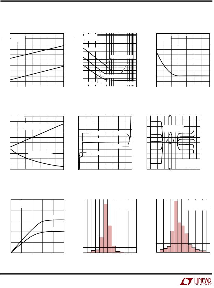
■100% Tested Low Voltage Noise: 3.2nV/√Hz Typ at 1kHz 4.5nV/√Hz Max at 1kHz
■Offset Voltage: 60 V Max
■Low VOS Drift: 0.2 V/°C Typ
■Low Input Bias Current: 20nA Max
■Wide Supply Range: 3V to ±18V
■High AVOL: 7V/ V Min, RL = 10k
■High CMRR: 109dB Min
■High PSRR: 108dB Min
■Gain Bandwidth Product: 7.2MHz
■Slew Rate: 2.5V/ s
■Operating Temperature Range: – 40°C to 85°C
APPLICATIOUS
■Low Noise Signal Processing
■Microvolt Accuracy Threshold Detection
■Strain Gauge Amplifiers
■Tape Head Preamplifiers
■Direct Coupled Audio Gain Stages
■Infrared Detectors
■Battery-Powered Microphones
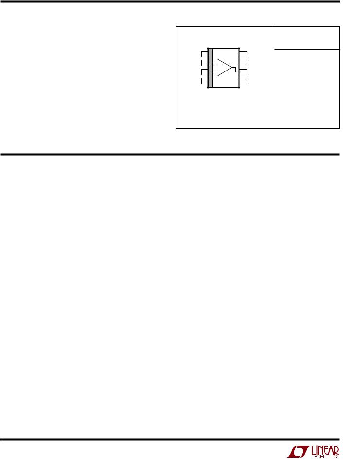
LT1677
Low Noise, Rail-to-Rail
Precision Op Amp
DESCRIPTIOU
The LT®1677 features the lowest noise performance avail- able for a rail-to-rail operational amplifier: 3.2nV/√Hz wideband noise, 1/f corner frequency of 13Hz and 90nV peak-to-peak 0.1Hz to 10Hz noise. Low noise is combined with outstanding precision: 20 V offset voltage and 0.2 V/°C drift, 130dB common mode and power supply rejection and 7.2MHz gain bandwidth product. The common mode range exceeds the power supply by 100mV.
The voltage gain of the LT1677 is extremely high, 19 million (typical) driving a 10k load.
In the design, processing and testing of the device, particular attention has been paid to the optimization of the entire distribution of several key parameters. Consequently, the specifications have been spectacularly improved compared to competing rail-to-rail amplifiers.
, LTC and LT are registered trademarks of Linear Technology Corporation.
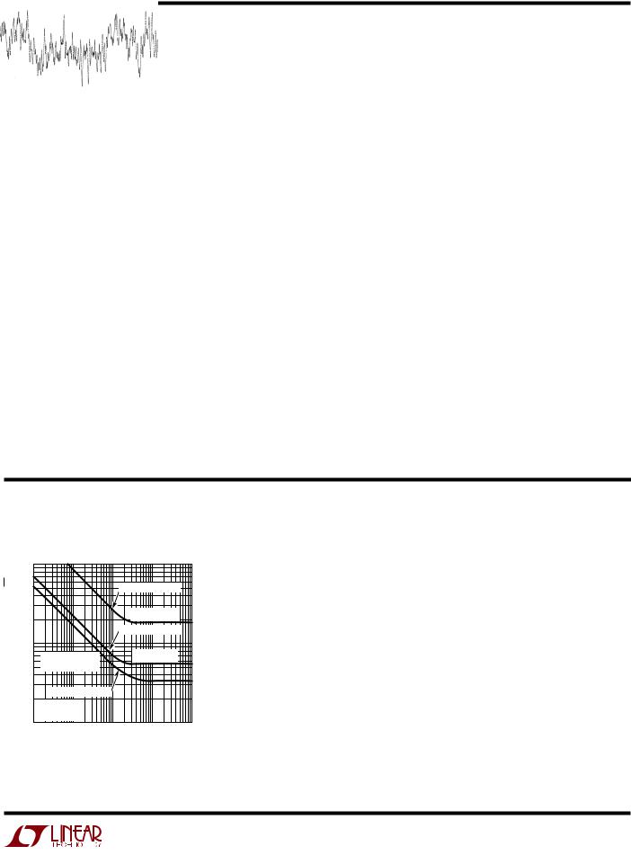
TYPICAL APPLICATIOU
3V Electret Microphone Amplifier
|
|
1.5V |
|
AV = –100 |
|
R3 |
|
|
|
|
|
|
|
|||||||||||||||
|
|
|
|
|
|
|
|
|
|
|
|
1M |
|
|
|
|
|
|
|
|||||||||
|
R1 |
|
|
|
|
C1 |
|
|
|
|
|
|
|
|
|
|
|
|
|
|
|
|
||||||
|
|
|
|
|
|
|
|
|
|
|
|
|
|
|
|
|
|
|
|
|
|
|
||||||
|
|
|
|
|
R2 |
|
|
|
|
|
1.5V |
|
|
|
|
|
|
|
||||||||||
PANASONIC |
10k |
|
|
|
|
0.68 F |
|
|
|
|
|
|
TO PA |
|||||||||||||||
|
|
|
|
|
|
|
|
|
|
|
|
|||||||||||||||||
ELECTRET |
|
|
|
|
|
|
|
|
|
|
10k |
2 |
– |
|
7 |
|
|
OR |
||||||||||
CONDENSER |
|
|
|
|
|
|
|
|
|
|
|
|
|
|
|
|
|
|
|
|
6 |
HEADPHONES |
||||||
MICROPHONE |
|
|
|
|
|
|
|
|
|
|
|
|
|
|
|
|
|
|
|
LT1677 |
|
|
|
|
|
|
|
|
|
|
|
|
|
|
|
|
|
|
|
|
|
|
|
|
|
|
|
|
|
|
|
|
|
|
|
||
WM-61 |
|
|
|
|
|
|
|
|
|
23Hz |
3 |
+ |
|
|
|
|
|
|
|
|
|
|||||||
|
|
|
|
|
|
|
|
|
|
|
|
|
|
|
|
|
|
|||||||||||
www.panasonic.com/pic |
|
|
|
|
|
|
|
|
|
|
|
|
|
|
4 |
|
|
|
|
|
|
|
||||||
|
|
|
|
|
|
|
|
|
|
|
|
|
|
|
|
|
|
|
|
|
||||||||
(714) 373-7334 |
|
|
|
|
|
|
|
|
|
HIGHPASS |
|
|
|
|
|
|
|
|
|
|
|
|
|
|
||||
|
|
|
|
|
|
|
|
|
|
|
|
|
|
|
|
|
|
|
|
|
|
|
|
|
|
|
||
|
|
|
|
|
|
|
|
|
|
|
|
|
|
|
|
|
|
|
|
–1.5V |
|
1677 TA01 |
|
|
|
|
||
|
|
|
|
|
|
|
|
|
|
|
|
|
|
|
|
|
|
|
|
|
|
|
|
|
|
|
||
Distribution of Offset Voltage
|
25 |
|
|
|
|
|
|
|
|
|
|
|
|
|
|
|
|
|
|
|
|
|
|
TA = 25°C |
|
|
|
|
|
|
|
|
|
|
|
|
|
|
|
||||||
|
|
|
|
|
|
|
|
|
|
|
|
|
|
|
|
|||||||
|
|
VS = ±15V |
|
|
|
|
|
|
|
|
|
|
|
|
|
|
||||||
UNITSOF |
20 |
|
|
|
|
|
|
|
|
|
|
|
|
|
|
|
|
|
|
|
|
|
|
|
|
|
|
|
|
|
|
|
|
|
|
|
|
|
|
|
|
|
|
||
15 |
|
|
|
|
|
|
|
|
|
|
|
|
|
|
|
|
|
|
|
|
|
|
|
|
|
|
|
|
|
|
|
|
|
|
|
|
|
|
|
|
|
|
|
||
|
|
|
|
|
|
|
|
|
|
|
|
|
|
|
|
|
|
|
|
|
||
|
|
|
|
|
|
|
|
|
|
|
|
|
|
|
|
|
|
|
|
|
||
PERCENT |
|
|
|
|
|
|
|
|
|
|
|
|
|
|
|
|
|
|
|
|
|
|
10 |
|
|
|
|
|
|
|
|
|
|
|
|
|
|
|
|
|
|
|
|
|
|
|
|
|
|
|
|
|
|
|
|
|
|
|
|
|
|
|
|
|
|
|
||
|
|
|
|
|
|
|
|
|
|
|
|
|
|
|
|
|
|
|
|
|
|
|
|
5 |
|
|
|
|
|
|
|
|
|
|
|
|
|
|
|
|
|
|
|
|
|
|
|
|
|
|
|
|
|
|
|
|
|
|
|
|
|
|
|
|
|
|
|
|
|
0 |
|
|
|
|
|
|
|
|
|
|
|
|
|
|
|
|
|
|
|
|
|
|
|
|
|
|
|
|
|
|
|
|
|
|
|
|
|
|
|
|
|
|
|
|
|
–40 |
–30 |
|
–20 |
–10 |
0 |
10 |
20 |
30 |
40 |
||||||||||||
INPUT OFFSET VOLTAGE ( V)
1677 TA02
1
LT1677
ABSOLUTE WAXIWUW RATIUGS
(Note 1)
Supply Voltage ...................................................... |
|
±22V |
Input Voltages (Note 2) ............ |
0.3V Beyond Either Rail |
|
Differential Input Current (Note 2) ..................... |
± 25mA |
|
Output Short-Circuit Duration (Note 3) ............ |
Indefinite |
|
Storage Temperature Range ................. |
|
– 65°C to 150°C |
Lead Temperature (Soldering, 10 sec.)................. |
300°C |
|
Operating Temperature Range |
|
– 40°C to 85°C |
LT1677C (Note 4) ............................. |
|
|
LT1677I ............................................. |
|
– 40°C to 85°C |
Specified Temperature Range |
|
– 40°C to 85°C |
LT1677C (Note 5) ............................. |
|
|
LT1677I ............................................. |
|
– 40°C to 85°C |
PACKAGE/ORDER IUFORWATIOU
|
|
|
|
|
ORDER PART |
|
|
|
TOP VIEW |
|
|
NUMBER |
|
VOS |
1 |
|
8 |
VOS |
LT1677CN8 |
|
TRIM |
– |
TRIM |
||||
–IN |
2 |
7 |
+VS |
LT1677CS8 |
||
+IN |
3 |
+ |
6 |
OUT |
||
LT1677IN8 |
||||||
–VS |
4 |
|
5 |
NC |
||
|
LT1677IS8 |
|||||
|
|
|
|
|
N8 PACKAGE |
|
S8 PACKAGE |
|
|
|
S8 PART MARKING |
|||
8-LEAD PDIP |
8-LEAD PLASTIC SO |
|||
|
||||
TJMAX = 150°C, θJA = |
150°C/ W (N8) |
|
||
1677 |
||||
TJMAX = 150°C, θJA = |
190°C/ W (S0-8) |
|||
1677I
Consult factory for Military grade parts.
temperature range, otherwise specifications are at TA otherwise noted.
The ● denotes the specifications which apply over the full operating = 25°C. VS = 3V, VCM = VO = 1.7V; VS = 5V, VCM = VO = 2.5V unless
SYMBOL |
PARAMETER |
CONDITIONS (Note 6) |
|
MIN |
TYP |
MAX |
UNITS |
||
|
|
|
|
|
|
|
|
|
|
VOS |
Input Offset Voltage (Note 11) |
|
|
|
35 |
90 |
µV |
||
|
|
|
|
0°C ≤ TA ≤ 70°C |
● |
|
55 |
150 |
µV |
|
|
|
|
– 40°C ≤ TA ≤ 85°C |
● |
|
75 |
210 |
µV |
|
|
|
|
VCM = VS + 0.1V |
|
|
150 |
400 |
µV |
|
|
|
|
VCM = VS – 0.2V, 0°C ≤ TA ≤ 70°C |
● |
|
180 |
550 |
µV |
|
|
|
|
VCM = VS – 0.3V, – 40°C ≤ TA ≤ 85°C |
● |
|
200 |
650 |
µV |
|
|
|
|
VCM = – 0.1V |
|
|
1.5 |
5.0 |
mV |
|
|
|
|
VCM = 0V, 0°C ≤ TA ≤ 70°C |
● |
|
1.8 |
6.0 |
mV |
|
|
|
|
VCM = 0V, – 40°C ≤ TA ≤ 85°C |
● |
|
2.0 |
6.5 |
mV |
VOS |
Average Input Offset Drift (Note 10) |
SO-8 |
● |
|
0.40 |
2.0 |
µV/°C |
||
Temp |
|
|
N8 |
● |
|
0.20 |
1.5 |
µV/°C |
|
VOS |
Long Term Input Voltage Stability |
|
|
|
0.3 |
|
µV/Mo |
||
Time |
|
|
|
|
|
|
|
|
|
IB |
Input Bias Current (Note 11) |
|
|
|
±2 |
±20 |
nA |
||
|
|
|
|
0°C ≤ TA ≤ 70°C |
● |
|
±3 |
±35 |
nA |
|
|
|
|
– 40°C ≤ TA ≤ 85°C |
● |
|
±7 |
±50 |
nA |
|
|
|
|
VCM = VS + 0.1V |
|
|
0.19 |
0.40 |
µA |
|
|
|
|
VCM = VS – 0.2V, 0°C ≤ TA ≤ 70°C |
● |
|
0.19 |
0.60 |
µA |
|
|
|
|
VCM = VS – 0.3V, – 40°C ≤ TA ≤ 85°C |
● |
|
0.25 |
0.75 |
µA |
|
|
|
|
VCM = – 0.1V |
|
– 1.2 |
– 0.41 |
|
µA |
|
|
|
|
VCM = 0V, 0°C ≤ TA ≤ 70°C |
● |
–2.0 |
– 0.45 |
|
µA |
|
|
|
|
VCM = 0V, – 40°C ≤ TA ≤ 85°C |
● |
–2.3 |
– 0.47 |
|
µA |
IOS |
Input Offset Current (Note 11) |
0°C ≤ TA ≤ 70°C |
|
|
4 |
15 |
nA |
||
|
|
|
|
● |
|
5 |
20 |
nA |
|
|
|
|
|
– 40°C ≤ TA ≤ 85°C |
● |
|
8 |
40 |
nA |
|
|
|
|
VCM = VS + 0.1V |
|
|
6 |
30 |
nA |
|
|
|
|
VCM = VS – 0.2V, 0°C ≤ TA ≤ 70°C |
● |
|
10 |
40 |
nA |
|
|
|
|
VCM = VS – 0.3V, – 40°C ≤ TA ≤ 85°C |
● |
|
15 |
65 |
nA |
|
|
|
|
VCM = – 0.1V |
|
|
20 |
100 |
nA |
|
|
|
|
VCM = 0V, 0°C ≤ TA ≤ 70°C |
● |
|
25 |
150 |
nA |
|
|
|
|
VCM = 0V, – 40°C ≤ TA ≤ 85°C |
● |
|
30 |
160 |
nA |
2

LT1677
temperature range, otherwise specifications are at TA otherwise noted.
The ● denotes the specifications which apply over the full operating = 25°C. VS = 3V, VCM = VO = 1.7V; VS = 5V, VCM = VO = 2.5V unless
SYMBOL |
PARAMETER |
CONDITIONS (Note 6) |
|
MIN |
TYP |
MAX |
UNITS |
|
|
|
|
|
|
|
|
|
|
|
|
en |
Input Noise Voltage |
0.1Hz to 10Hz (Note 7) |
|
|
90 |
|
nVP-P |
||
|
|
VCM = VS |
|
|
180 |
|
nVP-P |
||
|
|
VCM = 0V |
|
|
600 |
|
nVP-P |
||
|
Input Noise Voltage Density (Note 8) |
fO = 10Hz |
|
|
5.2 |
|
nV/√ |
|
|
|
|
|
|
Hz |
|||||
|
|
VCM = VS, fO = 10Hz |
|
|
7 |
|
nV/√Hz |
||
|
|
VCM = 0V, fO = 10Hz |
|
|
25 |
|
nV/√Hz |
||
|
|
fO = 1kHz |
|
|
3.2 |
4.5 |
nV/√ |
|
|
|
|
|
|
Hz |
|||||
|
|
VCM = VS, fO = 1kHz |
|
|
5.3 |
|
nV/√Hz |
||
|
|
VCM = 0V, fO = 1kHz |
|
|
17 |
|
nV/√Hz |
||
in |
Input Noise Current Density |
fO = 10Hz |
|
|
1.2 |
|
pA/√ |
|
|
|
|
|
Hz |
||||||
|
|
fO = 1kHz |
|
|
0.3 |
|
pA/√Hz |
||
VCM |
Input Voltage Range |
0°C ≤ TA ≤ 70°C |
|
– 0.1 |
|
VS + 0.1V |
|
V |
|
|
|
● |
0 |
|
VS – 0.2V |
|
V |
||
|
|
–40°C ≤ TA ≤ 85°C |
● |
0 |
|
VS – 0.3V |
|
V |
|
RIN |
Input Resistance |
Common Mode |
|
|
2 |
|
GΩ |
|
|
CIN |
Input Capacitance |
|
|
|
4.2 |
|
|
pF |
|
CMRR |
Common Mode Rejection Ratio (Note 11) |
VS = 3V |
|
|
|
|
|
|
|
|
|
VCM = –0.1V to 3.1V |
|
59 |
68 |
|
|
dB |
|
|
|
VCM = 0V to 2.7V |
● |
58 |
67 |
|
|
dB |
|
|
|
VS = 5V |
|
|
|
|
|
|
|
|
|
VCM = –0.1V to 5.1V |
|
63 |
73 |
|
|
dB |
|
|
|
VCM = 0V to 4.7V |
● |
62 |
72 |
|
|
dB |
|
PSRR |
Power Supply Rejection Ratio |
VS = 2.7V to 40V, VCM = VO = 1.7V |
|
108 |
125 |
|
|
dB |
|
|
|
VS = 3.1V to 40V, VCM = VO = 1.7V |
● |
105 |
120 |
|
|
dB |
|
AVOL |
Large-Signal Voltage Gain |
VS = 3V, RL ≥ 10k, VO = 2.5V to 0.7V |
|
0.6 |
4 |
|
V/µV |
|
|
|
|
0°C ≤ TA ≤ 70°C |
● |
0.4 |
3 |
|
V/µV |
||
|
|
–40°C ≤ TA ≤ 85°C |
● |
0.4 |
3 |
|
V/µV |
|
|
|
|
VS = 3V, RL ≥ 2k, VO = 2.2V to 0.7V |
|
0.5 |
1 |
|
V/µV |
||
|
|
0°C ≤ TA ≤ 70°C |
● |
0.4 |
0.9 |
|
V/µV |
||
|
|
–40°C ≤ TA ≤ 85°C |
● |
0.4 |
0.8 |
|
V/µV |
|
|
|
|
VS = 3V, RL ≥ 600Ω, VO = 2.2V to 0.7V |
|
0.20 |
0.43 |
|
V/µV |
||
|
|
0°C ≤ TA ≤ 70°C |
● |
0.15 |
0.40 |
|
V/µV |
||
|
|
–40°C ≤ TA ≤ 85°C |
● |
0.10 |
0.35 |
|
V/µV |
|
|
|
|
VS = 5V, RL ≥ 10k, VO = 4.5V to 0.7V |
|
0.8 |
5 |
|
V/µV |
||
|
|
0°C ≤ TA ≤ 70°C |
● |
0.7 |
4 |
|
V/µV |
||
|
|
–40°C ≤ TA ≤ 85°C |
● |
0.7 |
4 |
|
V/µV |
|
|
|
|
VS = 5V, RL ≥ 2k, VO = 4.2V to 0.7V |
|
0.40 |
0.9 |
|
V/µV |
||
|
|
0°C ≤ TA ≤ 70°C |
● |
0.35 |
0.8 |
|
V/µV |
||
|
|
–40°C ≤ TA ≤ 85°C |
● |
0.25 |
0.6 |
|
V/µV |
|
|
|
|
VS = 5V, RL ≥ 600Ω, VO = 4.2V to 0.7V |
|
0.35 |
0.67 |
|
V/µV |
||
|
|
0°C ≤ TA ≤ 70°C |
● |
0.30 |
0.60 |
|
V/µV |
||
|
|
–40°C ≤ TA ≤ 85°C |
● |
0.20 |
0.45 |
|
V/µV |
|
|
3

The ● denotes the specifications which apply over the full operating = 25°C. VS = 3V, VCM = VO = 1.7V; VS = 5V, VCM = VO = 2.5V unless
SYMBOL |
PARAMETER |
CONDITIONS (Note 6) |
|
MIN |
TYP |
MAX |
UNITS |
|
|
|
|
|
|
|
|
VOL |
Output Voltage Swing Low (Note 11) |
Above GND |
|
|
|
|
|
|
|
ISINK = 0.1mA |
|
|
110 |
170 |
mV |
|
|
0°C ≤ TA ≤ 70°C |
● |
|
125 |
200 |
mV |
|
|
– 40°C ≤ TA ≤ 85°C |
● |
|
130 |
230 |
mV |
|
|
Above GND |
|
|
|
|
|
|
|
ISINK = 2.5mA |
|
|
170 |
250 |
mV |
|
|
0°C ≤ TA ≤ 70°C |
● |
|
195 |
320 |
mV |
|
|
– 40°C ≤ TA ≤ 85°C |
● |
|
205 |
350 |
mV |
|
|
Above GND |
|
|
|
|
|
|
|
ISINK = 10mA |
|
|
370 |
500 |
mV |
|
|
0°C ≤ TA ≤ 70°C |
● |
|
440 |
600 |
mV |
|
|
– 40°C ≤ TA ≤ 85°C |
● |
|
465 |
650 |
mV |
VOH |
Output Voltage Swing High (Note 11) |
Below VS |
|
|
|
|
|
|
|
ISOURCE = 0.1mA |
|
|
75 |
170 |
mV |
|
|
0°C ≤ TA ≤ 70°C |
● |
|
85 |
200 |
mV |
|
|
– 40°C ≤ TA ≤ 85°C |
● |
|
93 |
250 |
mV |
|
|
Below VS |
|
|
|
|
|
|
|
ISOURCE = 2.5mA |
|
|
170 |
300 |
mV |
|
|
0°C ≤ TA ≤ 70°C |
● |
|
195 |
350 |
mV |
|
|
– 40°C ≤ TA ≤ 85°C |
● |
|
205 |
375 |
mV |
|
|
Below VS |
|
|
|
|
|
|
|
ISOURCE = 10mA |
|
|
450 |
700 |
mV |
|
|
0°C ≤ TA ≤ 70°C |
● |
|
510 |
800 |
mV |
|
|
– 40°C ≤ TA ≤ 85°C |
● |
|
525 |
850 |
mV |
ISC |
Output Short-Circuit Current (Note 3) |
VS = 3V |
|
15 |
22 |
|
mA |
|
|
0°C ≤ TA ≤ 70°C |
● |
14 |
20 |
|
mA |
|
|
– 40°C ≤ TA ≤ 85°C |
● |
13 |
19 |
|
mA |
|
|
VS = 5V |
|
20 |
29 |
|
mA |
|
|
0°C ≤ TA ≤ 70°C |
● |
18 |
27 |
|
mA |
|
|
– 40°C ≤ TA ≤ 85°C |
● |
17 |
25 |
|
mA |
SR |
Slew Rate (Note 13) |
AV = – 1 |
|
1.7 |
2.5 |
|
V/µs |
|
|
RL ≥ 10k, 0°C ≤ TA ≤ 70°C |
● |
1.5 |
2.3 |
|
V/µs |
|
|
RL ≥ 10k, – 40°C ≤ TA ≤ 85°C |
● |
1.2 |
2.0 |
|
V/µs |
GBW |
Gain Bandwidth Product (Note 11) |
fO = 100kHz |
|
4.5 |
7.2 |
|
MHz |
|
|
fO = 100kHz, 0°C ≤ TA ≤ 70°C |
● |
3.8 |
6.2 |
|
MHz |
|
|
fO = 100kHz, – 40°C ≤ TA ≤ 85°C |
● |
3.7 |
5.8 |
|
MHz |
tS |
Settling Time |
2V Step 0.1%, AV = +1 |
|
|
2.1 |
|
µs |
|
|
2V Step 0.01%, AV = +1 |
|
|
3.5 |
|
µs |
RO |
Open-Loop Output Resistance |
IOUT = 0 |
|
|
80 |
|
Ω |
|
Closed-Loop Output Resistance |
AV = 100, f = 10kHz |
|
|
1 |
|
Ω |
IS |
Supply Current (Note 12) |
0°C ≤ TA ≤ 70°C |
|
|
2.60 |
3.4 |
mA |
|
|
● |
|
2.75 |
3.7 |
mA |
|
|
|
– 40°C ≤ TA ≤ 85°C |
● |
|
2.80 |
3.8 |
mA |
4

LT1677
ELECTRICAL CHARACTERISTICS The ● denotes the specifications which apply over the full operating temperature range, otherwise specifications are at TA = 25°C. VS = ±15V, VCM = VO = 0V unless otherwise noted.
SYMBOL |
PARAMETER |
CONDITIONS (Note 6) |
|
MIN |
TYP |
MAX |
UNITS |
|
|||||
|
|
|
|
|
|
|
|
|
|
|
|
|
|
VOS |
Input Offset Voltage |
|
|
|
20 |
60 |
µV |
||||||
|
|
|
|
0°C ≤ TA ≤ 70°C |
● |
|
30 |
120 |
µV |
||||
|
|
|
|
– 40°C ≤ TA ≤ 85°C |
● |
|
45 |
180 |
µV |
|
|||
|
|
|
|
VCM = 15.1V |
|
|
150 |
400 |
µV |
||||
|
|
|
|
VCM = 14.8V, 0°C ≤ TA ≤ 70°C |
● |
|
180 |
550 |
µV |
||||
|
|
|
|
VCM = 14.7V, – 40°C ≤ TA ≤ 85°C |
● |
|
200 |
650 |
µV |
|
|||
|
|
|
|
VCM = – 15.1V |
|
|
1.5 |
5.0 |
mV |
||||
|
|
|
|
VCM = –15V, 0°C ≤ TA ≤ 70°C |
● |
|
1.8 |
6.0 |
mV |
||||
|
|
|
|
VCM = –15V, – 40°C ≤ TA ≤ 85°C |
● |
|
2.0 |
6.5 |
mV |
|
|||
VOS |
Average Input Offset Drift (Note 10) |
SO-8 |
● |
|
0.40 |
2.0 |
µV/°C |
||||||
Temp |
|
|
N8 |
● |
|
0.20 |
1.5 |
µV/°C |
|
||||
VOS |
Long Term Input Voltage Stability |
|
|
|
0.3 |
|
µV/Mo |
||||||
Time |
|
|
|
|
|
|
|
|
|
|
|
|
|
IB |
Input Bias Current |
0°C ≤ TA ≤ 70°C |
|
|
±2 |
±20 |
nA |
||||||
|
|
|
|
● |
|
±3 |
±35 |
nA |
|||||
|
|
|
|
– 40°C ≤ TA ≤ 85°C |
● |
|
±7 |
±50 |
nA |
||||
|
|
|
|
VCM = 15.1V |
|
|
0.19 |
0.40 |
µA |
|
|||
|
|
|
|
VCM = 14.8V, 0°C ≤ TA ≤ 70°C |
● |
|
0.20 |
0.60 |
µA |
||||
|
|
|
|
VCM = 14.7V, – 40°C ≤ TA ≤ 85°C |
● |
|
0.25 |
0.75 |
µA |
|
|||
|
|
|
|
VCM = –15.1V |
|
– 1.2 |
– 0.42 |
|
µA |
||||
|
|
|
|
VCM = –15V, 0°C ≤ TA ≤ 70°C |
● |
–2.0 |
– 0.46 |
|
µA |
||||
|
|
|
|
VCM = –15V, – 40°C ≤ TA ≤ 85°C |
● |
–2.3 |
– 0.48 |
|
µA |
|
|||
IOS |
Input Offset Current |
0°C ≤ TA ≤ 70°C |
|
|
3 |
15 |
nA |
||||||
|
|
|
|
● |
|
5 |
20 |
nA |
|||||
|
|
|
|
– 40°C ≤ TA ≤ 85°C |
● |
|
8 |
40 |
nA |
||||
|
|
|
|
VCM = 15.1V |
|
|
5 |
25 |
nA |
||||
|
|
|
|
VCM = 14.8V, 0°C ≤ TA ≤ 70°C |
● |
|
8 |
35 |
nA |
||||
|
|
|
|
VCM = 14.7V, – 40°C ≤ TA ≤ 85°C |
● |
|
12 |
60 |
nA |
||||
|
|
|
|
VCM = –15.1V |
|
|
20 |
105 |
nA |
||||
|
|
|
|
VCM = –15V, 0°C ≤ TA ≤ 70°C |
● |
|
25 |
160 |
nA |
||||
|
|
|
|
VCM = –15V, – 40°C ≤ TA ≤ 85°C |
● |
|
30 |
170 |
nA |
||||
en |
Input Noise Voltage |
0.1Hz to 10Hz (Note 7) |
|
|
90 |
|
nVP-P |
|
|||||
|
|
|
|
VCM = 15V |
|
|
180 |
|
nVP-P |
||||
|
|
|
|
VCM = –15V |
|
|
600 |
|
nVP-P |
||||
|
|
|
Input Noise Voltage Density |
fO = 10Hz |
|
|
5.2 |
|
nV/√ |
|
|
|
|
|
|
|
|
|
|
Hz |
|||||||
|
|
|
|
VCM = 15V, fO = 10Hz |
|
|
7 |
|
nV/√Hz |
||||
|
|
|
|
VCM = –15V, fO = 10Hz |
|
|
25 |
|
nV/√ |
Hz |
|
||
|
|
|
|
fO = 1kHz |
|
|
3.2 |
4.5 |
nV/√ |
|
|
||
|
|
|
|
|
|
Hz |
|||||||
|
|
|
|
VCM = 15V, fO = 1kHz |
|
|
5.3 |
|
nV/√Hz |
||||
|
|
|
|
VCM = –15V, fO = 1kHz |
|
|
17 |
|
nV/√Hz |
|
|||
in |
Input Noise Current Density |
fO = 10Hz |
|
|
1.2 |
|
pA/√ |
|
|
||||
|
|
|
Hz |
||||||||||
|
|
|
|
fO = 1kHz |
|
|
0.3 |
|
pA/√Hz |
||||
VCM |
Input Voltage Range |
0°C ≤ TA ≤ 70°C |
|
– 15.1 |
|
15.1 |
|
|
V |
|
|||
|
|
|
|
● |
– 15.0 |
|
14.8 |
|
|
V |
|||
|
|
|
|
–40°C ≤ TA ≤ 85°C |
● |
– 15.0 |
|
14.7 |
|
|
V |
|
|
RIN |
Input Resistance |
Common Mode |
|
|
2 |
|
GΩ |
|
|||||
CIN |
Input Capacitance |
|
|
|
4.2 |
|
|
|
pF |
|
|||
5

LT1677
ELECTRICAL CHARACTERISTICS The ● denotes the specifications which apply over the full operating temperature range, otherwise specifications are at TA = 25°C. VS = ±15V, VCM = VO = 0V unless otherwise noted.
SYMBOL |
PARAMETER |
CONDITIONS (Note 6) |
|
MIN |
TYP |
MAX |
UNITS |
|
|
|
|
|
|
|
|
CMRR |
Common Mode Rejection Ratio |
VCM = –13.3V to 14V |
|
109 |
130 |
|
dB |
|
|
|
● |
105 |
124 |
|
dB |
|
|
VCM = –15.1V to 15.1V |
|
74 |
95 |
|
dB |
|
|
VCM = –15V to 14.7V |
● |
72 |
91 |
|
dB |
PSRR |
Power Supply Rejection Ratio |
VS = ±1.7V to ±18V |
|
106 |
130 |
|
dB |
|
|
|
● |
103 |
125 |
|
dB |
|
|
VS = 2.7V to 40V |
|
108 |
125 |
|
dB |
|
|
VS = 3.1V to 40V |
● |
105 |
120 |
|
dB |
AVOL |
Large-Signal Voltage Gain |
RL ≥ 10k, VO = ±14V |
|
7 |
19 |
|
V/µV |
|
|
0°C ≤ TA ≤ 70°C |
● |
4 |
13 |
|
V/µV |
|
|
–40°C ≤ TA ≤ 85°C |
● |
3 |
8 |
|
V/µV |
|
|
RL ≥ 2k, VO = ±13.5V |
|
0.50 |
0.75 |
|
V/µV |
|
|
0°C ≤ TA ≤ 70°C |
● |
0.30 |
0.67 |
|
V/µV |
|
|
–40°C ≤ TA ≤ 85°C |
● |
0.15 |
0.24 |
|
V/µV |
|
|
RL ≥ 600Ω, VO = ±10V |
|
0.2 |
0.5 |
|
V/µV |
VOL |
Output Voltage Swing Low |
Above – VS |
|
|
|
|
|
|
|
ISINK = 0.1mA |
|
|
110 |
170 |
mV |
|
|
0°C ≤ TA ≤ 70°C |
● |
|
125 |
200 |
mV |
|
|
– 40°C ≤ TA ≤ 85°C |
● |
|
130 |
230 |
mV |
|
|
Above – VS |
|
|
|
|
|
|
|
ISINK = 2.5mA |
|
|
170 |
250 |
mV |
|
|
0°C ≤ TA ≤ 70°C |
● |
|
195 |
320 |
mV |
|
|
– 40°C ≤ TA ≤ 85°C |
● |
|
205 |
350 |
mV |
|
|
Above – VS |
|
|
|
|
|
|
|
ISINK = 10mA |
|
|
370 |
500 |
mV |
|
|
0°C ≤ TA ≤ 70°C |
● |
|
440 |
600 |
mV |
|
|
– 40°C ≤ TA ≤ 85°C |
● |
|
450 |
650 |
mV |
VOH |
Output Voltage Swing High |
Below +VS |
|
|
|
|
|
|
|
ISOURCE = 0.1mA |
|
|
110 |
170 |
mV |
|
|
0°C ≤ TA ≤ 70°C |
● |
|
130 |
200 |
mV |
|
|
– 40°C ≤ TA ≤ 85°C |
● |
|
140 |
250 |
mV |
|
|
Below +VS |
|
|
|
|
|
|
|
ISOURCE = 2.5mA |
|
|
210 |
300 |
mV |
|
|
0°C ≤ TA ≤ 70°C |
● |
|
240 |
350 |
mV |
|
|
– 40°C ≤ TA ≤ 85°C |
● |
|
250 |
375 |
mV |
|
|
Below +VS |
|
|
|
|
|
|
|
ISOURCE = 10mA |
|
|
520 |
700 |
mV |
|
|
0°C ≤ TA ≤ 70°C |
● |
|
590 |
800 |
mV |
|
|
– 40°C ≤ TA ≤ 85°C |
● |
|
620 |
850 |
mV |
ISC |
Output Short-Circuit Current (Note 3) |
0°C ≤ TA ≤ 70°C |
|
25 |
35 |
|
mA |
|
|
● |
20 |
30 |
|
mA |
|
|
|
– 40°C ≤ TA ≤ 85°C |
● |
18 |
28 |
|
mA |
SR |
Slew Rate |
RL ≥ 10k (Note 9) |
|
1.7 |
2.5 |
|
V/µs |
|
|
RL ≥ 10k (Note 9) 0°C ≤ TA ≤ 70°C |
● |
1.5 |
2.3 |
|
V/µs |
|
|
RL ≥ 10k (Note 9) – 40°C ≤ TA ≤ 85°C |
● |
1.2 |
2.0 |
|
V/µs |
GBW |
Gain Bandwidth Product |
fO = 100kHz |
|
4.5 |
7.2 |
|
MHz |
|
|
fO = 100kHz, 0°C ≤ TA ≤ 70°C |
● |
3.8 |
6.2 |
|
MHz |
|
|
fO = 100kHz, – 40°C ≤ TA ≤ 85°C |
● |
3.7 |
5.8 |
|
MHz |
6
LT1677
ELECTRICAL CHARACTERISTICS The ● denotes the specifications which apply over the full operating temperature range, otherwise specifications are at TA = 25°C. VS = ±15V, VCM = VO = 0V unless otherwise noted.
SYMBOL |
PARAMETER |
CONDITIONS (Note 6) |
|
MIN |
TYP |
MAX |
UNITS |
|
|
|
|
|
|
|
|
|
|
THD |
Total Harmonic Distortion |
RL = 2k, AV = 1, fO = 1kHz, VO = 10VP-P |
|
|
0.0006 |
|
% |
|
tS |
Settling Time |
10V |
Step 0.1%, AV = +1 |
|
|
5 |
|
µs |
|
|
10V |
Step 0.01%, AV = +1 |
|
|
6 |
|
µs |
RO |
Open-Loop Output Resistance |
IOUT = 0 |
|
|
80 |
|
Ω |
|
|
Closed-Loop Output Resistance |
AV = 100, f = 10kHz |
|
|
1 |
|
Ω |
|
IS |
Supply Current |
0°C ≤ TA ≤ 70°C |
|
|
2.75 |
3.5 |
mA |
|
|
|
● |
|
3.00 |
3.9 |
mA |
||
|
|
– 40°C ≤ TA ≤ 85°C |
● |
|
3.10 |
4.0 |
mA |
|
Note 1: Absolute Maximum Ratings are those values beyond which the life of the device may be impaired.
Note 2: The inputs are protected by back-to-back diodes. Current limiting resistors are not used in order to achieve low noise. If differential input voltage exceeds ±1.4V, the input current should be limited to 25mA. If the common mode range exceeds either rail, the input current should be limited to 10mA.
Note 3: A heat sink may be required to keep the junction temperature below absolute maximum.
Note 4: The LT1677C and LT1677I are guaranteed functional over the Operating Temperature Range of – 40°C to 85°C.
Note 5: The LT1677C is guaranteed to meet specified performance from 0°C to 70°C. The LT1677C is designed, characterized and expected to meet specified performance from – 40°C to 85°C but is not tested or QA sampled at these temperatures. The LT1677I is guaranteed to meet specified performance from – 40°C to 85°C.
Note 6: Typical parameters are defined as the 60% yield of parameter distributions of individual amplifier; i.e., out of 100 LT1677s, typically 60 op amps will be better than the indicated specification.
Note 7: See the test circuit and frequency response curve for 0.1Hz to 10Hz tester in the Applications Information section of the LT1677 data sheet.
Note 8: Noise is 100% tested at ±15V supplies.
Note 9: Slew rate is measured in AV = – 1; input signal is ±7.5V, output measured at ±2.5V.
Note 10: This parameter is not 100% tested. VS = 3V and 5V limits are guaranteed by correlation to VS = ±15V test.
Note 11: VS = 5V limits are guaranteed by correlation to VS = 3V and VS = ±15V tests.
Note 12: VS = 3V limits are guaranteed by correlation to VS = 5V and VS = ±15V tests.
Note 13: Guaranteed by correlation to slew rate at VS = ±15V and GBW at VS = 3V and VS = ±15V tests.
TYPICAL PERFORWAUCE CHARACTERISTICS
RMS VOLTAGE NOISE DENSITY (nV/√Hz)
Voltage Noise vs Frequency
100
1/f CORNER 10Hz
VCM < –14.5V
1/f CORNER 8.5Hz
10
|
VCM |
|
VCM > 14.5V |
|
|
–13.5V TO 14.5V |
|
|
|
|
1/f CORNER 13Hz |
|
|
|
VS = ±15V |
|
|
|
|
TA = 25°C |
|
|
|
|
1 |
1 |
10 |
100 |
1000 |
0.1 |
||||
FREQUENCY (Hz)
|
0.1Hz to 10Hz Voltage Noise |
|
|
|
0.01Hz to 1Hz Voltage Noise |
|
|
||||||||||||||||
|
|
|
|
|
|
|
|
|
|
|
VOLTAGE NOISE (20nV/DIV) |
|
|
|
|
|
|
|
|
|
|
|
|
VOLTAGE NOISE (20nV/DIV) |
|
|
|
|
|
|
|
|
|
|
|
|
|
|
|
|
|
|
|
|
|
|
|
|
|
|
|
|
|
|
|
|
|
|
|
|
|
|
|
|
|
|
|
|
|
||
|
|
|
|
|
|
|
|
|
|
|
|
|
|
|
|
|
|
|
|
|
|
||
|
|
|
|
|
|
|
|
|
|
|
|
|
|
|
|
|
|
|
|
|
|
||
|
|
|
|
|
|
|
|
|
|
|
|
|
|
|
|
|
|
|
|
|
|
||
|
|
|
|
|
|
|
|
|
|
|
|
|
|
|
|
|
|
|
|
|
|
||
|
|
|
|
|
|
|
|
|
|
|
|
|
|
|
|
|
|
|
|
|
|
||
|
|
|
|
|
|
|
|
|
|
|
|
|
|
|
|
|
|
|
|
|
|
||
|
|
|
|
|
|
|
|
|
|
|
|
|
|
|
|
|
|
|
|
|
|
|
|
|
|
|
|
|
|
|
|
|
|
|
|
|
|
|
|
|
|
|
|
|
|
|
|
0 |
2 |
4 |
6 |
8 |
10 |
0 |
20 |
40 |
60 |
80 |
100 |
||||||||||||
|
|
|
|
TIME (SECONDS) |
|
|
|
|
|
|
|
|
TIME (SECONDS) |
|
|
|
|
||||||
1677 G01 |
1677 G03 |
1677 G04 |
7
LT1677
TYPICAL PERFORWAUCE CHARACTERISTICS
RMS VOLTAGE NOISE DENSITY (nV/√Hz)
Voltage Noise vs Temperature
7
VS = ±15V
VCM = 0V
6
10Hz
5
4
1kHz
3
2 –50 –25 0 25 50 75 100 125
TEMPERATURE (°C)
1677 G08
RMS CURRENT NOISE DENSITY (pA/√Hz)
Current Noise vs Frequency
10
VS = ±15V
TA = 25°C
|
|
|
VCM < –13.5V |
|
|
|
|
|
|
|
|
|
|
|
|
|
|
|
|
|
|
|
|
|
|
|
|
|
|
|
|
1 |
|
|
|
|
|
|
1/f CORNER 180Hz |
|
|
|
|
|
|||
|
|
|
|
|
|
|
|
|
|
|
|
|
|
|
|
|
|
|
|
|
|
|
|
VCM |
|
|
|
|
|
||
|
|
|
|
|
|
|
|
|
|
|
|
|
|
||
|
|
|
|
|
|
|
|
–13.5V TO 14.5V |
|
||||||
|
|
|
|
|
|
|
|
|
|
|
|
|
|
|
|
|
|
|
|
1/f CORNER 90Hz |
|
|
|
|
|
|
|||||
|
|
|
|
|
|
|
|
||||||||
|
|
|
|
VCM > 14.5V |
|
||||||||||
0.1 |
|
1/f CORNER 60Hz |
|
|
|
|
|||||||||
|
|
|
|
|
|
||||||||||
|
|
|
|
|
|
|
|
|
|
|
|
|
|
|
|
|
100 |
|
|
|
1000 |
|
10000 |
||||||||
10 |
|
|
|
|
|||||||||||
FREQUENCY (Hz)
1677 G07
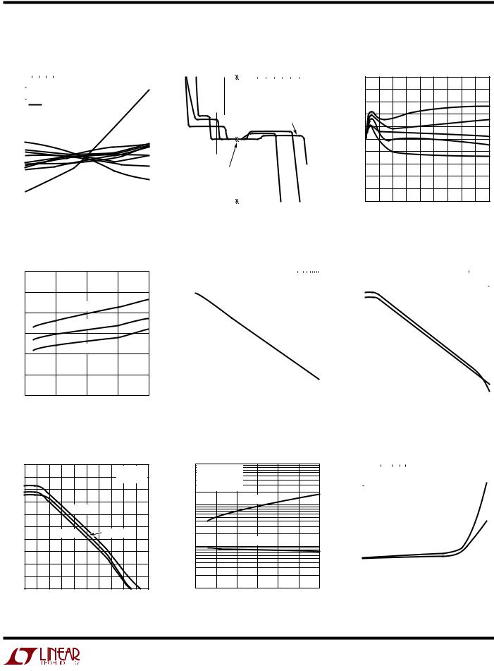
INPUT BIAS CURRENT (nA)
Input Bias Current vs Temperature
10
VS = ±15V 9 VCM = 0V
8
7
6
5
4
3
2
1
0 –50 –25 0 25 50 75 100 125
TEMPERATURE (°C)
1677 G05
INPUT BIAS CURRENT (nA)
Input Bias Current |
Input Bias Current Over the |
Offset Voltage Shift |
vs Temperature |
Common Mode Range |
vs Common Mode |
600 |
|
|
|
|
|
|
|
|
800 |
VS = ±15V |
|
|
|
|
|
|
|
2.5 |
|
|
|
|
|
|
|
|
250 |
|
||
VS = ±15V |
|
|
|
|
|
|
|
|
|
|
|
|
|
|
|
2.0 |
|
|
|
|
|
|
|
|
200 |
|
||||
|
|
|
|
|
|
|
|
|
600 |
|
|
° |
|
|
|
|
|
|
|
|
|
|
|
|
|
|
|
|
||
|
|
|
|
VCM = –14V |
|
|
|
TA = 25 C |
|
|
|
|
|
|
|
|
|
|
|
|
|
|
|
|
|
|
||||
500 |
|
|
|
|
|
CURRENTBIASINPUT(nA) |
|
|
|
|
|
|
|
|
|
|
|
1.5 |
|
|
|
VOS IS REFERRED |
|
|
150 |
|
||||
|
CURRENT OUT OF DUT |
|
|
400 |
|
|
|
|
|
|
|
|
|
(mV)VOLTAGEOFFSET |
|
|
|
|
|
|
||||||||||
|
|
|
CURRENT INTO DUT |
|
|
|
|
VCM = –13.6V |
VCM = 15.15V |
|
1.0 |
|
|
|
|
TO VCM = 0V |
|
|
100 |
V)(VOLTAGEOFFSET |
||||||||||
|
|
|
|
|
–400 |
|
|
|
|
|
|
|
|
|
|
|
||||||||||||||
400 |
|
|
|
|
|
|
|
|
200 |
|
|
|
|
|
|
|
|
|
|
0.5 |
|
|
|
|
|
|
|
|
50 |
|
|
|
|
|
|
|
|
|
|
|
|
INPUT BIAS CURRENT |
|
|
|
|
|
|
|
|
|
|
|
|
|||||||
|
|
|
|
|
|
|
|
|
0 |
|
|
|
|
|
0 |
|
|
|
|
|
|
|
|
0 |
|
|||||
|
|
|
|
|
|
|
|
|
|
|
|
|
|
VCM = 14.3V |
|
|
|
|
|
|
|
|
|
|
|
|
||||
300 |
|
|
|
|
|
|
|
|
–200 |
|
|
|
|
|
|
|
|
–0.5 |
|
|
|
|
|
|
|
|
–50 |
|
||
|
|
|
|
|
|
|
|
|
|
|
|
|
|
|
|
|
|
|
|
|
|
|
|
|
|
|
||||
|
|
|
|
|
|
|
|
|
|
VCM = –15.3V |
|
|
|
|
|
|
|
|
|
|
|
|
|
|
|
|
|
|||
|
|
|
VCM = 14.7V |
|
|
|
|
|
|
|
|
|
|
|
|
–1.0 |
|
|
|
|
|
|
|
|
–100 |
|
||||
200 |
|
|
|
|
|
|
|
|
|
|
|
|
|
|
|
|
|
|
|
–1.5 |
|
|
|
|
|
|
|
|
–150 |
|
|
|
|
|
|
|
|
|
|
–600 |
|
|
|
|
|
|
|
|
|
|
|
|
|
|
|
|
VS = ±1.5V TO ±15V |
|
|||
|
|
|
|
|
|
|
|
|
|
|
|
|
|
|
|
|
|
|
–2.0 |
|
|
|
|
|
TA = 25°C |
|
–200 |
|
||
|
|
|
|
|
|
|
|
|
|
|
|
|
|
|
|
|
|
|
|
|
|
|
|
|
|
|
||||
100 |
|
|
|
|
|
|
|
|
–800 |
|
|
|
|
|
|
|
|
|
|
–2.5 |
|
|
|
|
|
5 TYPICAL PARTS |
|
|||
–25 |
0 |
25 |
50 |
75 |
100 |
125 |
|
|
–12 |
–8 |
–4 |
0 |
4 |
8 |
12 |
16 |
|
V– |
1.0 |
2.0 |
–0.8 –0.4 |
|
V+ |
–250 |
|
|||||
–50 |
|
–16 |
|
–1.0 |
|
0.4 |
|
|||||||||||||||||||||||
|
|
|
|
|
° |
|
|
|
|
|
COMMON MODE INPUT VOLTAGE (V) |
|
|
|
VCM – V |
– |
(V) |
|
VCM – V |
+ |
(V) |
|
|
|||||||
|
|
TEMPERATURE ( C) |
|
|
|
|
|
|
|
|
|
|
|
|
|
|||||||||||||||
|
|
|
|
|
|
1677 G06 |
|
|
|
|
|
|
|
|
|
1677 G09 |
|
|
|
|
|
|
|
|
|
|
1677 G10 |
|
||
CHANGE IN OFFSET VOLTAGE ( V)
Warm-Up Drift
10
VS = ±15V
TA = 25°C
8
SO PACKAGE
6
N PACKAGE
4
2
0
0 |
1 |
2 |
3 |
4 |
5 |
TIME (MINUTES)
1677 G02
PERCENT OF UNITS (%)
|
Distribution of Input Offset |
|||||||
|
Voltage Drift (N8) |
|||||||
50 |
|
|
|
|
|
|
|
|
|
|
|
|
|
|
|
|
|
|
|
|
|
|
VS = ±15V |
|
||
45 |
|
|
|
|
|
|
||
|
|
|
|
|
TA = –40°C TO 85°C |
|
||
40 |
|
|
|
|
|
167 PARTS (4 LOTS) |
|
|
|
|
|
|
|
|
|
|
|
|
|
|
|
|
|
|
|
|
35 |
|
|
|
|
|
|
|
|
|
|
|
|
|
|
|
|
|
30 |
|
|
|
|
|
|
|
|
|
|
|
|
|
|
|
|
|
25 |
|
|
|
|
|
|
|
|
|
|
|
|
|
|
|
|
|
20 |
|
|
|
|
|
|
|
|
|
|
|
|
|
|
|
|
|
15 |
|
|
|
|
|
|
|
|
|
|
|
|
|
|
|
|
|
|
|
|
|
|
|
|
|
|
10 |
|
|
|
|
|
|
|
|
|
|
|
|
|
|
|
|
|
|
|
|
|
|
|
|
|
|
5
0 

 –1.0 –0.6 –0.2 0.2 0.6 1.0 1.4
INPUT OFFSET VOLTAGE DRIFT ( V/°C)
1677 G13
PERCENT OF UNITS (%)
Distribution of Input Offset
Voltage Drift (SO-8)
30 |
|
|
|
|
|
|
|
|
|
|
|
|
|
VS = ±15V |
|
||
|
|
|
|
|
|
|
||
25 |
|
|
|
|
|
TA = –40°C TO 85°C |
|
|
|
|
|
|
|
201 PARTS (5 LOTS) |
|
||
|
|
|
|
|
||||
20 |
|
|
|
|
|
|
|
|
|
|
|
|
|
|
|
|
|
15 |
|
|
|
|
|
|
|
|
|
|
|
|
|
|
|
|
|
10 |
|
|
|
|
|
|
|
|
|
|
|
|
|
|
|
|
|
|
|
|
|
|
|
|
||
|
|
|
|
|
|
|
|
|
5
0 
 –0.8 –0.4 0 0.4 0.8 1.2 1.6 2.0
INPUT OFFSET VOLTAGE DRIFT ( V/°C)
1677 G37
8
LT1677
TYPICAL PERFORWAUCE CHARACTERISTICS
VOLTAGE OFFSET ( V)
VOS vs Temperature of |
|
|
Common Mode Range |
|
|
|
|
|
|||||||||||||||||||||||||||||||||||||||||
Representative Units |
|
|
vs Temperature |
|
|
|
|
|
|
|
|
|
|
|
|
|
|
|
|
||||||||||||||||||||||||||||||
140 |
|
|
|
|
|
|
|
|
|
|
|
|
|
|
|
|
|
|
|
|
|
|
|
2.5 |
|
|
|
|
|
|
|
|
|
|
|
|
|
|
|
|
|
|
|
|
|
|
|
250 |
|
120 |
|
VS = ±15V |
|
|
|
|
|
|
|
|
|
|
|
|
|
|
|
|
|
|
|
|
|
|
|
|
|
|
|
VS = ±2.5V TO ± |
15V |
|
|
||||||||||||||||
|
|
VCM = 0V |
|
|
|
|
|
|
|
|
|
|
|
|
|
|
|
|
2.0 |
|
|
|
|
|
|
|
|
|
|
|
|
|
|
|
|
|
|
|
|
|
|
|
200 |
|
|||||
100 |
|
|
|
|
SO-8 |
|
|
|
|
|
|
|
|
|
|
|
|
|
|
|
|
1.5 |
|
|
|
|
|
|
|
|
|
|
|
|
|
|
|
|
|
|
|
|
|
|
|
150 |
|
||
|
|
|
|
|
|
|
|
|
|
|
|
|
|
|
|
|
|
|
|
|
|
|
|
|
|
|
|
|
|
|
|
|
|
|
|
|
|
|
|
|
|
|
|
||||||
|
|
|
|
|
|
|
|
|
|
|
|
|
|
|
|
|
|
|
|
|
|
|
|
|
|
|
|
|
|
|
|
|
|
|
|
|
|
|
|
|
|
|
|||||||
80 |
|
|
|
|
N8 |
|
|
|
|
|
|
|
|
|
|
|
|
|
|
|
VOLTAGEOFFSET(mV) |
|
|
|
125°C |
|
|
|
|
|
|
|
|
|
|
|
|
|
|
|
|
|
V)(VOLTAGEOFFSET |
||||||
|
|
|
|
|
|
|
|
|
|
|
|
|
|
|
|
|
|
|
|
|
|
|
|
|
|
|
|
|
|
|
|
|
|
|
|
|
|
|
|
|
|||||||||
–20 |
|
|
|
|
|
|
|
|
|
|
|
|
|
|
|
|
|
|
|
|
|
|
–1.0 |
|
|
|
|
|
|
TO VCM |
= |
0V |
|
|
|
|
|
|
|
|
|
|
|
|
|
–100 |
|||
60 |
|
|
|
|
|
|
|
|
|
|
|
|
|
|
|
|
|
|
|
|
|
|
|
1.0 |
|
|
|
|
|
|
25°C |
|
|
|
|
|
|
|
|
|
|
–55°C |
|
100 |
|
||||
40 |
|
|
|
|
|
|
|
|
|
|
|
|
|
|
|
|
|
|
|
|
|
|
|
0.5 |
|
–55°C |
|
|
|
|
|
|
|
|
|
|
|
|
|
|
|
|
|
|
|
50 |
|
||
20 |
|
|
|
|
|
|
|
|
|
|
|
|
|
|
|
|
|
|
|
|
|
|
|
0 |
|
|
|
|
|
|
|
|
|
|
|
|
|
|
|
|
|
|
|
|
|
|
|
0 |
|
|
|
|
|
|
|
|
|
|
|
|
|
|
|
|
|
|
|
|
|
|
|
|
–0.5 |
|
|
|
|
|
|
|
|
|
|
|
|
|
|
|
|
|
|
|
|
|
|
|
–50 |
|
|
0 |
|
|
|
|
|
|
|
|
|
|
|
|
|
|
|
|
|
|
|
|
|
|
|
|
|
|
|
|
|
|
|
|
|
|
|
|
|
|
|
|
|
|
|
|
|
|
|
||
|
|
|
|
|
|
|
|
|
|
|
|
|
|
|
|
|
|
|
|
|
|
|
|
|
|
|
|
VOS IS REFERRED |
|
125°C |
|
|
|
|
|
|
|
|
|
|
|||||||||
|
|
|
|
|
|
|
|
|
|
|
|
|
|
|
|
|
|
|
|
|
|
|
|
|
|
|
|
|
|
|
|
|
|
|
|
|
|
|
|
||||||||||
–40 |
|
|
|
|
|
|
|
|
|
|
|
|
|
|
|
|
|
|
|
|
|
|
|
–1.5 |
|
|
|
|
|
|
|
|
|
|
|
|
|
|
|
|
25°C |
|
|
|
–150 |
|
|||
|
|
|
|
|
|
|
|
|
|
|
|
|
|
|
|
|
|
|
|
|
|
|
|
|
|
|
|
|
|
|
|
|
|
|
|
|
|
||||||||||||
|
|
|
|
|
|
|
|
|
|
|
|
|
|
|
|
|
|
|
|
|
|
|
|
|
|
|
|
|
|
|
|
|
|
|
|
|
|
|
|
|
|
|
|
|
|
|
|||
|
|
|
|
|
|
|
|
|
|
|
|
|
|
|
|
|
|
|
|
|
|
|
|
|
|
|
|
|
|
|
|
|
|
|
|
|
|
|
|
|
|
|
|
|
|
|
|||
|
|
|
|
|
|
|
|
|
|
|
|
|
|
|
|
|
|
|
|
|
|
|
|
|
|
|
|
|
|
|
|
|
|
|
|
|
|
|
|
|
|
|
|
|
|
|
|||
–60 |
|
|
|
|
|
|
|
|
|
|
|
|
|
|
|
|
|
|
|
|
|
|
|
–2.0 |
|
|
|
|
|
|
|
|
|
|
|
|
|
|
|
|
|
|
|
|
|
|
|
–200 |
|
|
|
|
|
|
|
|
|
|
|
|
|
|
|
|
|
|
|
|
|
|
|
|
|
|
|
|
|
|
|
|
|
|
|
|
|
|
|
|
|
|
|
|
|
|
|
|
|||
–80 |
|
|
|
|
|
|
|
|
|
|
|
|
|
|
|
|
|
|
|
|
|
|
|
–2.5 |
|
|
|
|
|
|
|
|
|
|
|
|
|
|
|
|
|
|
|
|
|
|
|
–250 |
|
|
|
–35 –15 5 25 45 65 85 105 125 |
|
|
|
|
|
|
|
|
|
|
–0.8 |
|
–0.4 V+ |
0.4 |
|
||||||||||||||||||||||||||||||||
–55 |
|
–1.0 V– 1.0 2.0 |
|
|
|
||||||||||||||||||||||||||||||||||||||||||||
|
|
|
|
|
|
|
|
|
TEMPERATURE (°C) |
|
|
|
VCM – VS– (V) |
|
VCM – VS+ (V) |
|
|
|
|
|
|||||||||||||||||||||||||||||
|
|
|
|
|
|
|
|
|
|
|
|
|
|
|
|
|
|
|
1677 G11 |
|
|
|
|
|
|
|
|
|
|
|
|
|
|
|
|
|
|
|
|
|
1677 G12 |
|
|||||||
OFFSET VOLTAGE CHANGE ( V)
Long-Term Stability of Four
Representative Units
5
4
3
2
1
0
–1
–2
–3
–4
–5
0 100 200 300 400 500 600 700 800 900 TIME (HOURS)
1677 G14
SUPPLY CURRENT (mA)
Supply Current vs Supply Voltage
4
TA = 125°C
3
TA = 25°C
TA = –55°C
2
1 |
±5 |
±10 |
±15 |
±20 |
0 |
SUPPLY VOLTAGE (V)
1677 G15
COMMON MODE REJECTION RATIO (dB)
|
Common Mode Rejection Ratio |
|
|
|
|||||||||||||||||||||||||
|
vs Frequency |
|
|
|
|
|
|
|
|
|
|
|
|
|
|
|
|
|
|||||||||||
160 |
|
|
|
|
|
|
|
|
|
|
|
|
|
|
|
|
|
|
|
|
|
|
|
|
|
|
|
|
|
|
|
|
|
|
|
|
|
|
|
|
|
|
|
|
|
|
|
|
|
|
VS = ±15V |
|
|||||||
|
|
|
|
|
|
|
|
|
|
|
|
|
|
|
|
|
|
|
|
|
|
|
|||||||
140 |
|
|
|
|
|
|
|
|
|
|
|
|
|
|
|
|
|
|
|
|
|
TA = 25°C |
|
||||||
|
|
|
|
|
|
|
|
|
|
|
|
|
|
|
|
|
|
|
|
|
|
||||||||
|
|
|
|
|
|
|
|
|
|
|
|
|
|
|
|
|
|
|
|
|
|
VCM = 0V |
|
||||||
120 |
|
|
|
|
|
|
|
|
|
|
|
|
|
|
|
|
|
|
|
|
|
|
|
|
|
|
|
|
|
|
|
|
|
|
|
|
|
|
|
|
|
|
|
|
|
|
|
|
|
|
|
|
|
|
|
|
|
|
|
100 |
|
|
|
|
|
|
|
|
|
|
|
|
|
|
|
|
|
|
|
|
|
|
|
|
|
|
|
|
|
|
|
|
|
|
|
|
|
|
|
|
|
|
|
|
|
|
|
|
|
|
|
|
|
|
|
|
|
|
|
80 |
|
|
|
|
|
|
|
|
|
|
|
|
|
|
|
|
|
|
|
|
|
|
|
|
|
|
|
|
|
|
|
|
|
|
|
|
|
|
|
|
|
|
|
|
|
|
|
|
|
|
|
|
|
|
|
|
|
|
|
60 |
|
|
|
|
|
|
|
|
|
|
|
|
|
|
|
|
|
|
|
|
|
|
|
|
|
|
|
|
|
|
|
|
|
|
|
|
|
|
|
|
|
|
|
|
|
|
|
|
|
|
|
|
|
|
|
|
|
|
|
40 |
|
|
|
|
|
|
|
|
|
|
|
|
|
|
|
|
|
|
|
|
|
|
|
|
|
|
|
|
|
|
|
|
|
|
|
|
|
|
|
|
|
|
|
|
|
|
|
|
|
|
|
|
|
|
|
|
|
|
|
20 |
|
|
|
|
|
|
|
|
|
|
|
|
|
|
|
|
|
|
|
|
|
|
|
|
|
|
|
|
|
|
|
|
|
|
|
|
|
|
|
|
|
|
|
|
|
|
|
|
|
|
|
|
|
|
|
|
|
|
|
0 |
|
|
|
|
|
|
|
|
|
|
|
|
|
|
|
|
|
|
|
|
|
|
|
|
|
|
|
|
|
|
|
|
|
|
|
10k |
|
|
|
|
|
|
|
|
|
|
|
|
|
|
|
|
|
||||||
1k |
100k |
1M |
10M |
||||||||||||||||||||||||||
FREQUENCY (Hz)
1677 G16
POWER SUPPLY REJECTION RATIO (dB)
Power Supply Rejection Ratio vs Frequency
160 |
|
|
|
|
|
|
|
|
|
|
|
|
|
|
|
|
|
|
|
|
|
|
|
VS = ±15V |
|
|
|||
|
|
|
|
|
|
|
|
|
|
|
|
|||
140 |
|
|
|
|
|
|
|
|
|
TA = 25°C |
|
|
|
|
|
|
|
|
|
|
|
|
|
|
|
|
|||
120 |
|
|
|
|
|
|
|
|
|
|
|
|
|
|
|
|
|
|
|
|
|
|
|
|
|
|
|
|
|
100 |
|
|
|
|
|
|
|
|
|
|
|
|
|
|
|
|
|
|
|
|
|
|
|
|
|
|
|
|
|
|
|
|
|
|
|
NEGATIVE SUPPLY |
|
|
|
|||||
80 |
|
|
|
|
|
|
|
|
|
|
|
|
|
|
60 |
|
POSITIVE |
SUPPLY |
|
|
|
|
|
|
|
|
|||
|
|
|
|
|
|
|
|
|
|
|
|
|
|
|
|
|
|
|
|
|
|
|
|
|
|
|
|
|
|
40 |
|
|
|
|
|
|
|
|
|
|
|
|
|
|
|
|
|
|
|
|
|
|
|
|
|
|
|
|
|
20 |
|
|
|
|
|
|
|
|
|
|
|
|
|
|
|
|
|
|
|
|
|
|
|
|
|
|
|
|
|
0 |
|
|
|
|
|
|
|
|
|
|
|
|
|
|
|
10 |
100 |
1k |
10k |
100k |
1M |
||||||||
1 |
||||||||||||||
FREQUENCY (Hz)
1677 G17
|
Voltage Gain vs Supply Voltage |
Voltage Gain vs Frequency |
(Single Supply) |
|
180 |
|
|
|
VS = ±15V |
|
100 |
TA = 25°C |
|
|
|
|
|
|
|
|
|
|
|
|
|||
|
|
|
|
|
TA = 25°C |
V) |
|
RL TO GND |
|
|
|
|
140 |
|
|
|
|
|
|
VCM: VO = VS/2 |
|
|
|
|
|
|
|
|
|
(V/ |
|
|
|
|
|
|
|
|
|
|
|
|
|
|
RL = 10k |
|
|
(dB) |
|
|
VCM = 0V |
|
|
|
GAIN |
10 |
|
|
|
|
|
|
|
|
|
|
|
||||
|
|
|
|
|
|
|
|
|
|
|
|
VOLTAGEGAIN |
100 |
|
|
|
|
|
VOLTAGELOOP |
|
|
|
|
60 |
VCM = VEE |
VCM = VCC |
|
|
|
RL = 2k |
|
||||
|
|
|
|
|
|
||||||
|
|
|
|
|
|
|
1 |
|
|
||
|
|
|
|
|
|
|
OPEN |
|
|
|
|
|
20 |
|
|
|
|
|
|
|
|
|
|
|
|
|
|
|
|
|
|
|
|
|
|
|
–20 |
|
|
|
|
|
|
0.1 |
10 |
20 |
30 |
|
0.01 |
1 |
100 |
10k |
1M |
100M |
|
0 |
|||
|
|
|
FREQUENCY (Hz) |
|
|
|
|
SUPPLY VOLTAGE (V) |
|
||
|
|
|
|
|
|
1677 G18 |
|
|
|
|
1677 G19 |
OVERSHOOT (%)
Overshoot vs Load Capacitance
60 |
|
|
|
|
|
|
|
|
|
|
|
|
|
|
|
|
|
|
|
|
|
|
|
VS = ±15V |
|
|
|
|
|
|
|
|
|
|
|
|
|
|
|
|
|
||||
|
|
|
|
|
|
|
|
|
|
|
|
|
|
|
|
|
|
|
||||
|
|
TA = 25°C |
|
|
|
|
|
|
|
|
|
|
|
|
|
|
|
|
|
|||
50 |
|
RL = 10k TO 2k |
|
|
|
|
|
|
|
|
|
|
|
|
|
|
|
|
|
|||
|
|
|
|
|
|
|
|
|
|
|
|
|
|
|
|
|
||||||
40 |
|
|
|
|
|
|
|
|
|
|
|
|
|
|
|
|
|
|
|
|
|
|
|
|
|
|
|
|
|
|
|
|
|
|
|
|
|
|
|
|
|
|
|
|
|
|
|
|
|
|
|
|
|
|
|
|
|
|
|
|
|
|
|
|
|
|
|
|
30 |
|
|
|
|
|
|
|
|
|
|
|
|
RISING |
|
|
|
|
|
|
|
||
|
|
|
|
|
|
|
|
|
|
|
|
|
EDGE |
|
|
|
|
|
|
|||
|
|
|
|
|
|
|
|
|
|
|
|
|
|
|
|
|
|
|
||||
20 |
|
|
|
|
|
|
|
|
|
|
|
|
|
|
|
|
|
|
|
|
|
|
|
|
|
|
|
|
|
|
|
|
|
|
|
|
|
|
|
|
|
|
|
|
|
|
|
|
|
|
|
|
|
|
|
|
|
|
|
|
|
|
|
|
|
|
|
|
|
|
|
|
|
|
|
|
|
|
|
|
|
|
FALLING |
|
|
|
|
||||
10 |
|
|
|
|
|
|
|
|
|
|
|
|
|
EDGE |
|
|
|
|||||
|
|
|
|
|
|
|
|
|
|
|
|
|
|
|
|
|||||||
0 |
|
|
|
|
|
|
|
|
|
|
|
|
|
|
|
|
|
|
|
|
|
|
|
|
|
|
|
|
|
|
|
|
|
|
|
|
|
|
|
|
|
|
|
|
|
|
|
|
|
|
|
|
|
100 |
1000 |
|||||||||||||
10 |
|
|
|
|
|
|
||||||||||||||||
CAPACITANCE (pF)
1677 G21
9
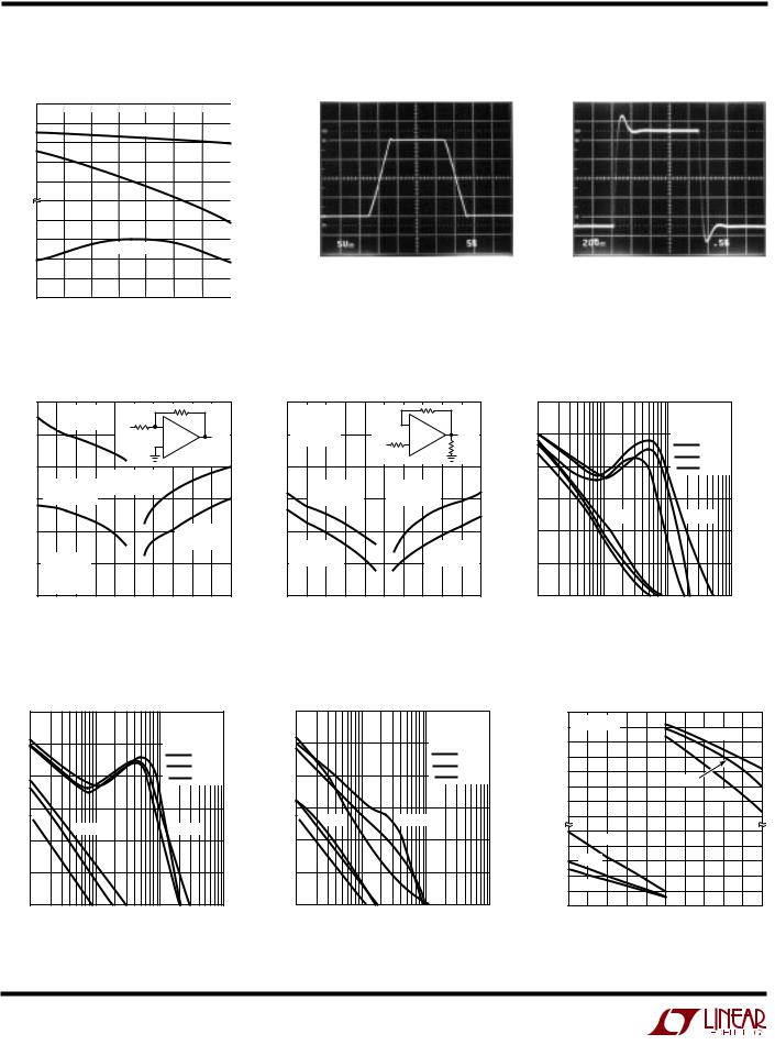
LT1677
TYPICAL PERFORWAUCE CHARACTERISTICS
SLEW RATE (V/ s) PHASE MARGIN (DEG)
PM, GBWP, SR vs Temperature
70
PHASE
60
GBW
50
3
SLEW
2
1 –50 –25 0 25 50
|
|
|
GAIN |
||
|
VS = ±15V |
|
|||
|
CL = 15pF |
|
BANDWIDTH |
||
|
|
|
8 |
||
|
|
|
|
||
|
|
|
7 |
PRODUCT, |
|
|
|
|
5 |
||
|
|
|
6 |
|
|
|
|
|
|
f |
|
|
|
|
4 |
O |
|
|
|
|
= |
||
|
|
|
|
(MHz) 100kHz |
|
75 |
100 |
125 |
|||
|
|||||
TEMPERATURE (°C)
1677 G22
Large-Signal Transient Response |
Small-Signal Transient Response |
||
10V |
|
50mV |
|
|
|
|
|
|
|
0 |
|
– 10V |
|
– 50mV |
|
|
|
|
|
AVCL = – 1 |
5 s/DIV |
AVCL = 1 |
0.5 s/DIV |
VS = ±15V |
|
VS = ±15V |
|
CL = 15pF
SETTLING TIME ( s)
Settling Time vs Output Step (Inverting)
12 |
|
|
|
0.01% OF |
5k |
5k |
|
FULL SCALE |
|||
VIN |
– |
||
10 |
|
VOUT |
|
|
|
+ |
|
8 |
|
|
0.01% OF
0.1% OF FULL SCALE
6 FULL SCALE
4 |
0.1% OF |
FULL SCALE
2VS = ±15V
AV = –1 °CTA = 25
0 |
–8 |
–6 |
–4 |
–2 |
0 |
2 |
4 |
6 |
8 |
10 |
–10 |
OUTPUT STEP (V)
1677 G25
Settling Time vs Output Step |
Gain, Phase Shift vs Frequency |
(Noninverting) |
|
12 |
VS = ±15V |
|
|
|
|
|
|
|
|
|
50 |
|
VS = ±15V |
100 |
|
|||
|
|
|
|
|
|
|
2k |
|
|
|
|
|
|
|
|||||
|
10 |
AV = 1 |
|
|
|
|
|
– |
|
|
|
40 |
|
VCM = 0V |
80 |
|
|||
|
|
|
° |
|
|
|
|
|
|
|
VOUT |
|
|
CL = 10pF |
|
||||
|
|
TA = 25 C |
|
|
V |
IN |
2k |
+ |
|
RL = 1k |
|
|
|
|
° |
|
|
||
|
|
|
|
|
|
|
|
|
|
|
|
|
|
125 C |
|
|
|||
s)(TIMESETTLING |
4 |
|
|
|
|
|
|
|
|
|
|
|
(dB)GAINVOLTAGE |
10 |
|
|
25°C |
20 |
(DEG)SHIFTPHASE |
|
8 |
|
|
|
|
|
|
|
|
|
|
|
|
30 |
|
|
° |
60 |
|
|
|
|
|
|
|
|
|
|
|
|
|
|
|
|
|
– 55 C |
|
|
|
|
|
|
|
0.01% OF |
|
|
|
0.01% OF |
|
|
|
|
|
|
|
|
|
||
|
6 |
|
FULL SCALE |
|
|
FULL SCALE |
|
|
20 |
|
|
|
40 |
|
|||||
|
|
|
|
|
|
|
|
|
|
|
|
|
|
|
GAIN |
|
PHASE |
|
|
|
|
|
0.1% OF |
|
|
|
|
|
|
0.1% OF |
|
|
|
|
|
|
|
||
|
2 |
FULL SCALE |
|
|
|
|
FULL SCALE |
0 |
|
|
|
0 |
|
||||||
|
0 |
|
–8 |
–6 |
–4 |
–2 |
|
0 |
2 |
4 |
6 |
8 |
10 |
–10 |
1 |
10 |
|
–20 |
|
|
–10 |
|
0.1 |
100 |
|
||||||||||||||
|
|
|
|
|
OUTPUT STEP (V) |
|
|
|
|
FREQUENCY (MHz) |
|
|
|
||||||
|
|
|
|
|
|
|
|
|
|
|
|
1677 G26 |
|
|
|
1677 G34 |
|
|
|
Gain, Phase Shift vs Frequency |
Gain, Phase Shift vs Frequency |
Output Voltage Swing |
vs Load Current |
|
50 |
|
VS = ±15V |
100 |
|
50 |
|
VS = ±15V |
100 |
+VS – 0 |
VS = ±15V |
|
|
|
|
|
|
|
|
||||||||
|
|
|
|
|
|
|
|
|
|
|
–0.1 |
|
|
|
|
|
° |
|
|
||||||||
|
|
|
V |
CM |
= 14.7V |
|
|
|
|
|
VCM = –14V |
|
|
|
|
|
|
|
|
|
|
|
|
|
|||
|
40 |
|
|
|
80 |
|
|
40 |
|
CL = 10pF |
80 |
|
|
–0.2 |
|
|
|
|
|
|
|
–55 C |
|
|
|||
|
|
CL = 10pF |
|
|
|
|
(V) |
|
|
|
|
|
|
|
|
|
|
|
|||||||||
|
|
|
|
|
125°C |
|
|
|
|
|
|
125°C |
|
|
–0.3 |
|
|
|
|
|
|
|
|
|
|
|
|
(dB)GAINVOLTAGE |
30 |
|
|
|
25°C |
60 |
(DEG)SHIFTPHASE |
(dB)GAINVOLTAGE |
30 |
|
|
25°C |
60 |
(DEG)SHIFTPHASE |
SWINGVOLTAGEOUTPUT |
0.3 |
|
25°C |
|
|
|
|
|
|
|
|
|
|
|
|
– 55°C |
|
|
– 55°C |
|
|
|
|
|
|
° |
|
|
|
|||||||||||
|
|
|
|
|
|
|
|
|
|
–0.4 |
|
|
|
|
|
|
|
|
|
|
|||||||
|
|
|
|
|
|
|
|
|
|
|
|
|
|
|
|
–0.5 |
|
|
|
|
|
|
25 C |
|
|
|
|
|
|
|
|
|
|
|
|
|
|
|
|
|
|
|
|
|
|
|
|
|
|
|
|
125°C |
|
|
|
|
|
|
|
|
|
|
|
|
|
|
|
|
|
|
|
–0.6 |
|
|
|
|
|
|
|
|
|
|
|
|
20 |
|
|
|
|
40 |
|
|
20 |
|
|
|
40 |
|
|
|
|
|
|
|
|
|
|
|
|
|
|
|
|
|
|
|
|
|
|
PHASE |
|
|
|
–0.7 |
|
|
|
|
|
|
|
|
|
|
|
||||
|
|
|
|
|
|
|
|
|
GAIN |
|
|
|
|
|
|
|
|
|
|
|
|
|
|
|
|
||
|
|
GAIN |
|
PHASE |
|
|
|
|
|
|
|
|
0.5 |
|
|
|
|
|
|
|
|
|
|
|
|||
|
10 |
|
20 |
|
|
10 |
|
|
|
20 |
|
|
|
125°C |
|
|
|
|
|
|
|
|
|||||
|
|
|
|
|
|
|
|
|
|
|
|
0.4 |
|
|
|
|
|
|
|
|
|
||||||
|
|
|
|
|
|
|
|
|
|
|
|
|
|
|
|
|
|
|
|
|
|
|
|
|
|
|
|
|
0 |
|
|
|
|
0 |
|
|
0 |
|
|
|
0 |
|
|
0.2 |
–55°C |
|
|
|
|
|
|
|
|
|
|
|
|
|
|
|
|
|
|
|
|
|
|
|
|
|
|
|
|
|
|
|
|
|
|
|
|||
|
|
|
|
|
|
|
|
|
|
|
|
|
|
|
|
0.1 |
|
|
|
|
|
|
|
|
|
||
|
|
|
|
|
|
|
|
|
|
|
|
|
|
|
|
|
|
|
|
|
|
|
|
|
|
|
|
–10 |
1 |
10 |
|
|
–20 |
–10 |
1 |
10 |
|
–20 |
–VS + 0 |
|
–8 |
–6 |
–4 |
–2 |
0 |
2 |
4 |
6 |
8 |
10 |
|||||
|
0.1 |
|
100 |
|
|
0.1 |
100 |
|
|
–10 |
|||||||||||||||||
|
|
FREQUENCY (MHz) |
|
|
|
|
|
|
FREQUENCY (MHz) |
|
|
|
|
|
|
ISINK |
|
|
|
|
ISOURCE |
|
|
||||
|
|
|
|
|
1677 G35 |
|
|
|
|
|
|
1677 G36 |
|
|
|
|
|
|
OUTPUT CURRENT (mA) |
1677 G27 |
|||||||
|
|
|
|
|
|
|
|
|
|
|
|
|
|
|
|
|
|
|
|
|
|
|
|
||||
10