

бакМИТ_КП2015 / Компоненты по вариантам / Операционные_усилители / LT1677IN8
.pdfLT1677
TYPICAL PERFORWAUCE CHARACTERISTICS
Closed-Loop Output Impedance vs Frequency
|
100 |
|
|
|
|
|
|
|
|
|
|
|
|
|
|
|
|
|
|
|
|
|
|
|
|
|
|
|
|
(Ω ) |
10 |
|
|
|
|
|
|
|
|
|
|
|
|
|
|
|
|
|
|
|
|
|
|
|
|
|
|
||
|
|
|
|
|
|
|
|
|
|
|
|
|
|
|
IMPEDANCE |
1 |
|
|
|
|
|
|
|
|
|
|
|
|
|
|
|
|
|
|
|
|
|
|
|
|
|
|
|
|
|
|
|
|
|
AV = |
+100 |
|
|
|
|
|
|
|
|
OUTPUT |
0.1 |
|
|
|
|
|
|
|
|
|
|
|
|
|
|
|
|
|
|
|
|
|
|
|
|
|
|
||
|
|
|
|
|
|
|
|
|
|
|
|
|
|
|
|
|
|
|
|
|
|
AV |
= +1 |
|
|
|
|
||
|
|
|
|
|
|
|
|
|
|
|
|
|||
|
0.01 |
|
|
|
|
|
|
|
|
|
|
|
|
|
|
|
|
|
|
|
|
|
|
|
|
|
|
|
|
|
0.001 |
|
|
|
|
|
|
|
|
|
|
|
|
|
|
|
100 |
1k |
10k |
100k |
1M |
||||||||
|
10 |
|||||||||||||
FREQUENCY (Hz)
1677 G29
|
|
|
Output Short-Circuit Current |
|||
|
|
|
vs Time |
|
||
|
|
50 |
V |
S |
= ±15V |
–55°C |
|
SOURCING |
40 |
|
|
||
|
|
|
|
|||
(mA)CURRENT |
|
|
|
|
||
30 |
|
|
|
25°C |
||
|
|
|
|
|
||
|
|
|
|
|
|
|
|
|
20 |
|
|
|
125°C |
|
|
10 |
|
|
|
|
|
|
|
|
|
|
|
CIRCUIT |
|
–30 |
|
|
|
° |
- |
|
–35 |
|
|
|
25 C |
SHORT |
SINKING |
|
|
|
125°C |
|
–40 |
|
|
|
–55°C |
||
|
|
|
|
|
||
|
|
–45 |
|
|
|
|
|
|
|
|
|
|
|
|
|
–50 |
|
|
|
|
0 1 2 3 4 TIME FROM OUTPUT SHORT TO GND (MIN)
1677 G28
Total Harmonic Distortion and
Noise vs Frequency for
Noninverting Gain
(%) |
0.1 |
|
|
|
|
|
|
|
|
|
|
|
|
|
|
|
|
|
|
|
|
|
|
|
|
|
|
|
|
|
|
|
|
|
|
|
|
ZL = 2k/15pF |
|
|
|
|
|
|
|
|
|
|
|
||||||||||||||||||
NOISE |
|
|
|
VS = ±15V |
|
|
|
|
|
|
|
|
|
|
|
||||||||||||||||||
|
|
|
|
|
|
|
|
|
|
|
|
|
|
||||||||||||||||||||
|
|
|
AV = +1, +10, +100 |
|
|
|
|
|
|
|
|
|
|
|
|||||||||||||||||||
+ |
|
|
|
VO = 10VP-P |
|
|
|
|
|
|
|
|
|
|
|
||||||||||||||||||
|
|
|
MEASUREMENT BANDWIDTH |
|
|
|
|
|
|
|
|
|
|||||||||||||||||||||
DISTROTION |
0.01 |
|
|
|
|
|
|
|
|
|
|
|
|||||||||||||||||||||
|
|
= 10Hz TO 80kHz |
|
|
|
|
|
|
|
|
|
|
|
||||||||||||||||||||
|
|
|
|
|
|
|
|
|
|
|
|
|
|
||||||||||||||||||||
|
|
|
|
|
|
|
|
|
|
|
|
|
|
||||||||||||||||||||
|
|
|
|
|
|
|
|
|
|
|
|
|
|
|
|
|
|
|
|
|
|
|
|
|
|
|
|
|
|
|
|
|
|
HARMONIC |
0.001 |
|
|
|
|
|
AV = 100 |
|
|
|
|
|
|
|
|
|
|
|
|
|
|
|
|
|
|
||||||||
|
|
|
|
|
|
|
|
|
|
|
|
|
|
|
|
|
|
|
|
|
|
|
|
|
|
|
|
|
|
|
|
||
|
|
|
|
|
|
|
|
|
|
|
|
|
|
|
|
|
|
|
|
|
|
|
|
|
|
|
|
|
|
|
|
||
|
|
|
|
|
|
|
|
|
|
|
|
|
|
|
|
|
|
|
|
|
|
|
|
|
|
|
|
|
|
|
|
||
|
|
|
|
|
|
|
AV = 10 |
|
|
|
|
|
|
|
|
|
|
|
|
|
|
|
|
|
|
|
|||||||
|
|
|
|
|
|
|
|
|
|
|
|
|
|
|
|
|
|
|
|
|
|
|
|
|
|||||||||
|
|
|
|
|
|
|
|
|
|
|
|
|
|
|
|
|
|
|
|
|
|
|
|
|
|||||||||
|
|
|
|
|
|
|
|
|
|
|
|
|
|
|
|
|
|
|
|
|
|
|
|
|
|
||||||||
|
|
|
|
|
|
|
|
|
|
|
|
|
|
|
|
|
|
|
|
|
|
|
|
|
|
|
|
|
|
|
|
|
|
TOTAL |
0.0001 |
|
|
|
|
|
|
AV = |
1 |
|
|
|
|
|
|
|
|
|
|
|
|
|
|
|
|
|
|
|
|
||||
|
|
|
|
|
|
|
|
|
|
|
|
|
|
|
|
|
|
|
|
|
|
|
|
|
|||||||||
|
|
|
|
|
|
|
|
|
|
|
|
|
|
|
|
|
|
|
|
|
|
|
|
|
|
|
|
|
|
|
|
||
|
|
|
100 |
|
|
|
|
|
|
|
|
|
|
|
|
|
|
|
|
|
|
|
|||||||||||
|
20 |
|
|
|
|
|
|
|
|
1k |
10k 20k |
||||||||||||||||||||||
FREQUENCY (Hz)
1677 G30
Total Harmonic Distortion and Noise vs Frequency for Inverting Gain
(%) |
0.1 |
|
|
|
|
|
|
|
|
|
|
|
|
|
|
|
|
|
|
|
|
|
|
|
|
|
|
|
|
|
|
|
|
|
|
|
|
ZL = 2k/15pF |
|
|
|
|
|
|
|
|
|
|
|
||||||||||||||||||
NOISE |
|
|
|
VS = ±15V |
|
|
|
|
|
|
|
|
|
|
|
||||||||||||||||||
|
|
|
|
|
|
|
|
|
|
|
|
|
|
||||||||||||||||||||
|
|
|
AV = –1, –10, – 100 |
|
|
|
|
|
|
|
|
|
|
|
|||||||||||||||||||
+ |
|
|
|
VO = 10VP-P |
|
|
|
|
|
|
|
|
|
|
|
||||||||||||||||||
|
|
|
MEASUREMENT BANDWIDTH |
|
|
|
|
|
|
|
|
|
|||||||||||||||||||||
DISTROTION |
0.01 |
|
|
|
|
|
|
|
|
|
|
|
|||||||||||||||||||||
|
|
= 10Hz TO 80kHz |
|
|
|
|
|
|
|
|
|
|
|
||||||||||||||||||||
|
|
|
|
|
|
|
|
|
|
|
|
|
|
||||||||||||||||||||
|
|
|
|
|
|
|
|
|
|
|
|
|
|
||||||||||||||||||||
|
|
|
|
|
|
|
|
|
|
|
|
|
|
|
|
|
|
|
|
|
|
|
|
|
|
|
|
|
|
|
|
|
|
HARMONIC |
0.001 |
|
|
|
AV = –100 |
|
|
|
|
|
|
|
|
|
|
|
|
|
|
|
|
|
|
||||||||||
|
|
|
|
|
|
|
|
|
|
|
|
|
|
|
|
|
|
|
|
|
|||||||||||||
|
|
|
|
|
|
|
|
|
|
|
|
|
|
|
|
|
|
|
|
|
|
|
|
|
|
|
|
|
|
|
|
||
|
|
|
|
|
|
|
|
|
|
|
|
|
|
|
|
|
|
|
|
|
|
|
|
|
|
|
|
|
|
|
|
||
|
|
|
|
|
|
|
|
|
|
|
|
|
|
|
|
|
|
|
|
|
|
|
|
|
|
|
|
|
|
|
|
||
|
|
|
|
|
AV = –10 |
|
|
|
|
|
|
|
|
|
|
|
|
|
|
|
|
|
|
|
|||||||||
|
|
|
|
|
|
|
|
|
|
|
|
|
|
|
|
|
|
|
|
|
|
|
|
|
|||||||||
|
|
|
|
|
|
|
|
|
|
|
|
|
|
|
|
|
|
|
|
|
|
|
|
|
|||||||||
|
|
|
|
|
|
|
|
|
|
|
|
|
|
|
|
|
|
|
|
|
|
|
|
|
|
|
|
|
|
|
|
|
|
|
|
|
|
|
|
|
|
|
|
|
|
|
|
|
|
|
|
|
|
|
|
|
|
|
|
|
|
|
|
|
|
|
|
TOTAL |
0.0001 |
|
|
|
|
|
|
A |
V |
|
= |
|
–1 |
|
|
|
|
|
|
|
|
|
|
|
|
|
|
|
|
|
|
|
|
|
|
|
|
|
|
|
|
|
|
|
|
|
|
|
|
|
|
|
|
|
|
|
|
||||||||||
|
|
|
|
|
|
|
|
|
|
|
|
|
|
|
|
|
|
|
|
|
|
|
|
|
|
|
|
|
|
|
|
||
|
|
|
100 |
|
|
|
|
|
|
|
|
|
|
|
|
|
|
|
|
|
|
|
|||||||||||
|
20 |
|
|
|
|
|
|
|
|
1k |
10k 20k |
||||||||||||||||||||||
FREQUENCY (Hz)
1677 G31
Total Harmonic Distortion and Noise vs Output Amplitude for Noninverting Gain
TOTAL HARMONIC DISTORTION + NOISE (%)
1
0.1
0.01
0.001
0.0001
0.3
ZL = 2k/15pF
VS = ±15V fO = 1kHz
AV = +1, +10, +100 MEASUREMENT BANDWIDTH = 10Hz TO 22kHz
AV = 100
AV = 10
AV = 1
1 |
10 |
30 |
OUTPUT SWING (VP-P)
1677 G32
Total Harmonic Distortion and Noise vs Output Amplitude for Inverting Gain
TOTAL HARMONIC DISTORTION + NOISE (%)
1
0.1
0.01
0.001
0.0001
0.3
ZL = 2k/15pF
VS = ±15V fO = 1kHz
AV = –1, –10, –100 MEASUREMENT BANDWIDTH = 10Hz TO 22kHz
AV = –100
AV = –10
AV = –1
1 |
10 |
30 |
OUTPUT SWING (VP-P)
1677 G33
11
LT1677
APPLICATIOUS IUFORWATIOU
General
The LT1677 series devices may be inserted directly into OP-07, OP-27, OP-37 and sockets with or without removal of external compensation or nulling components. In addition, the LT1677 may be fitted to 741 sockets with the removal or modification of external nulling components.
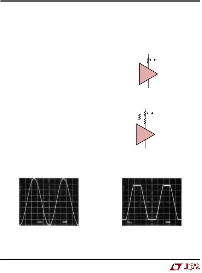
Rail-to-Rail Operation
To take full advantage of an input range that can exceed the supply, the LT1677 is designed to eliminate phase reversal. Referring to the photographs shown in Figure 1, the LT1677 is operating in the follower mode (AV = +1) at a single 3V supply. The output of the LT1677 clips cleanly and recovers with no phase reversal. This has the benefit of preventing lock-up in servo systems and minimizing distortion components.
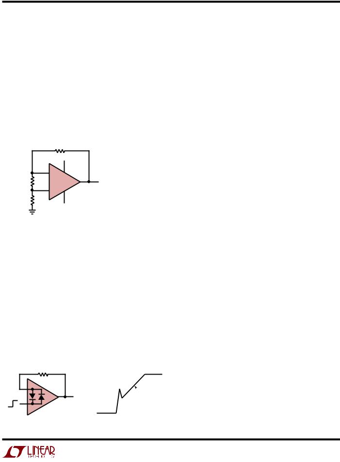
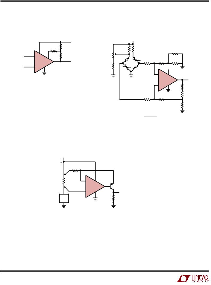
Offset Voltage Adjustment
The input offset voltage of the LT1677 and its drift with temperature are permanently trimmed at wafer testing to a low level. However, if further adjustment of VOS is necessary, the use of a 10kΩ nulling potentiometer will not degrade drift with temperature. Trimming to a value other than zero creates a drift of (VOS /300)µV/°C, e.g., if VOS is adjusted to 300µV, the change in drift will be 1µV/°C (Figure 2).
Input = – 0.5V to 3.5V
3V
2V
1V
0V
– 0.5V
1577 F01a
The adjustment range with a 10kΩ pot is approximately
±2.5mV. If less adjustment range is needed, the sensitivity and resolution of the nulling can be improved by using a smaller pot in conjunction with fixed resistors. The example has an approximate null range of ±200µV (Figure 3).
|
|
|
|
|
|
|
|
|
|
|
|
|
|
10k |
|
|
|
|
|
15V |
||||
|
|
|
|
2 |
|
|
|
1 |
|
|
|
|
|
|
|
|
|
|
|
|
||||
|
|
|
|
|
|
|
|
|
|
|
|
|
|
|
|
|
|
|||||||
|
|
|
|
|
|
|
|
|
|
|
|
|
|
|
|
|
|
|
|
|
||||
|
|
|
|
|
|
– |
|
|
|
|
8 |
|
|
7 |
6 |
|
|
|
OUTPUT |
|||||
|
|
|
|
LT1677 |
|
|
|
|||||||||||||||||
INPUT |
|
|
|
|
|
|
|
|
|
|
|
|
||||||||||||
|
|
|
|
|
|
|
|
|
|
|
|
|
||||||||||||
3 |
|
|
|
|
|
|
|
|
|
|
|
|
|
|||||||||||
|
|
|
|
|
+ |
|
|
|
|
|
|
|
|
|
|
|
|
|
|
|
||||
|
|
|
|
|
|
|
|
|
|
|
|
4 |
|
|
|
|
|
|
|
|
|
|||
|
|
|
|
|
|
|
|
|
|
|
–15V |
|
|
|
|
|
|
1677 F02 |
||||||
Figure 2. Standard Adjustment |
||||||||||||||||||||||||
|
|
|
4.7k |
|
|
|
|
|
1k |
|
|
|
15V |
|||||||||||
|
|
|
|
|
|
|
|
|
|
|
||||||||||||||
|
|
|
|
|
|
|
|
|
|
|
|
|
|
|
|
|
||||||||
|
|
|
|
|
|
|
|
|
|
|
|
|
|
|
|
|
||||||||
|
|
|
|
|
|
|
|
|
|
|
|
|
|
|
|
|
|
|
|
|
||||
|
|
|
|
|
|
|
|
|
|
|
|
4.7k |
|
|
|
|
|
|
|
|
|
|||
2 |
|
|
– |
|
|
|
|
|
|
|
|
|
|
|
6 |
|
|
|
|
OUTPUT |
||||
LT1677 |
|
|
|
|
|
|
||||||||||||||||||
|
|
|
|
|
|
|
|
|
|
|
|
|||||||||||||
|
|
|
|
|
|
|
|
|
|
|
|
|
||||||||||||
|
|
3 |
|
+ |
|
|
|
|
|
|
|
|||||||||||||
|
|
|
|
|
|
|
|
|
|
|
|
|
|
|
|
|
|
|
|
|||||
|
|
|
|
|
|
|
–15V |
|
|
|
|
|
|
1677 F03 |
||||||||||
|
|
|
|
|
|
|
|
|
|
|
|
|
|
|
||||||||||
Figure 3. Improved Sensitivity Adjustment
LT1677 Output
3V
2V
1V
0V
– 0.5V
1577 F01b
Figure 1. Voltage Follower with Input Exceeding the Supply Voltage (VS = 3V)
12
LT1677
APPLICATIOUS IUFORWATIOU
Offset Voltage and Drift
Thermocouple effects, caused by temperature gradients across dissimilar metals at the contacts to the input terminals, can exceed the inherent drift of the amplifier unless proper care is exercised. Air currents should be minimized, package leads should be short, the two input leads should be close together and maintained at the same temperature.
The circuit shown to measure offset voltage is also used as the burn-in configuration for the LT1677, with the supply voltages increased to ±20V (Figure 4).
|
|
50k* |
|
|
|
|
|
15V |
|
|
|
2 |
– |
7 |
|
|
|
|
|
6 |
|
||
100Ω* |
LT1677 |
VOUT |
|||
|
|||||
3 |
+ |
4 |
VOUT = 1000VOS |
||
50k* |
|
|
*RESISTORS MUST HAVE LOW |
||
|
|
THERMOELECTRIC POTENTIAL |
|||
|
|
–15V |
|||
|
|
|
|
||
|
|
|
|
1677 F04 |
|
Figure 4. Test Circuit for Offset Voltage and
Offset Voltage Drift with Temperature
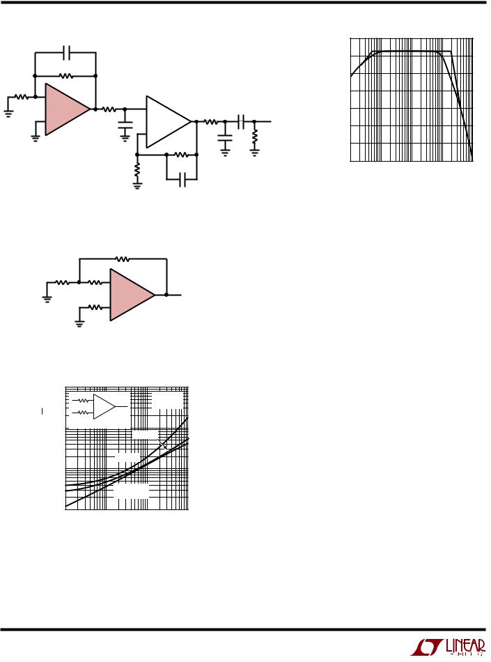
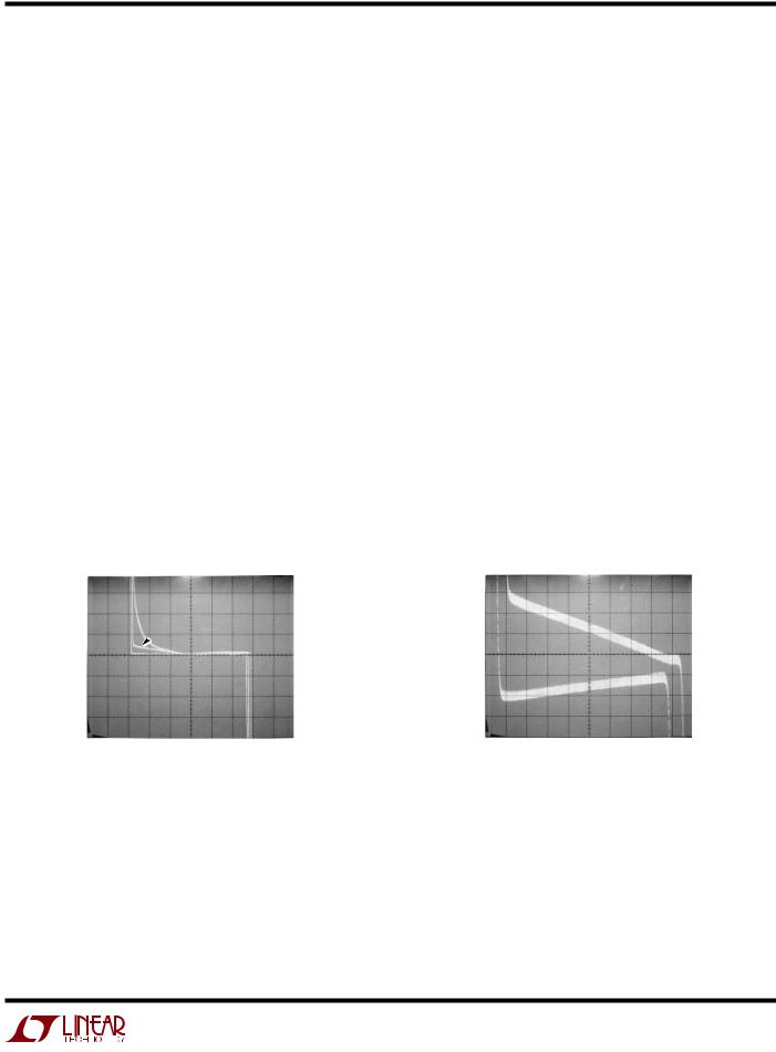
Unity-Gain Buffer Application
When RF ≤ 100Ω and the input is driven with a fast, largesignal pulse (>1V), the output waveform will look as shown in the pulsed operation diagram (Figure 5).
During the fast feedthrough-like portion of the output, the input protection diodes effectively short the output to the input and a current, limited only by the output short-circuit protection, will be drawn by the signal generator. With RF ≥ 500Ω, the output is capable of handling the current requirements (IL ≤ 20mA at 10V) and the amplifier stays in its active mode and a smooth transition will occur.
RF
–
OUTPUT
+LT1677
 2.5V/µs
1677 F05
Figure 5. Pulsed Operation
As with all operational amplifiers when RF > 2k, a pole will be created with RF and the amplifier’s input capacitance, creating additional phase shift and reducing the phase margin. A small capacitor (20pF to 50pF) in parallel with RF will eliminate this problem.
Noise Testing
The 0.1Hz to 10Hz peak-to-peak noise of the LT1677 is measured in the test circuit shown (Figure 6a). The frequency response of this noise tester (Figure 6b) indicates that the 0.1Hz corner is defined by only one zero. The test time to measure 0.1Hz to 10Hz noise should not exceed ten seconds, as this time limit acts as an additional zero to eliminate noise contributions from the frequency band below 0.1Hz.
Measuring the typical 90nV peak-to-peak noise performance of the LT1677 requires special test precautions:
1.The device should be warmed up for at least five
minutes. As the op amp warms up, its offset voltage changes typically 3µV due to its chip temperature increasing 10°C to 20°C from the moment the power supplies are turned on. In the ten-second measurement interval these temperature-induced effects can easily exceed tens of nanovolts.
2.For similar reasons, the device must be well shielded from air currents to eliminate the possibility of thermoelectric effects in excess of a few nanovolts, which would invalidate the measurements.
3.Sudden motion in the vicinity of the device can also “feedthrough” to increase the observed noise.
Current noise is measured in the circuit shown in Figure 7 and calculated by the following formula:
|
|
2 |
2 |
1/ 2 |
|
(eno) |
− (130nV •101) |
|
|
i = |
|
|
|
|
|
|
(1MΩ)(101) |
|
|
n |
|
|
||
|
|
|
|
|
The LT1677 achieves its low noise, in part, by operating the input stage at 100µA versus the typical 10µA of most other op amps. Voltage noise is inversely proportional while current noise is directly proportional to the square
13
LT1677
APPLICATIOUS IUFORWATIOU |
|
|
|||
0.1µF |
|
|
|
|
|
100k |
|
|
|
|
|
10Ω |
|
|
|
|
|
– |
2k |
|
|
|
|
* |
+ |
|
22µF |
|
|
LT1677 |
|
4.3k |
SCOPE |
||
+ |
|
LT1001 |
|
||
4.7µF |
|
|
× 1 |
||
|
|
– |
|
|
RIN = 1M |
VOLTAGE GAIN |
|
|
2.2µF |
110k |
|
|
|
100k |
|
|
|
= 50,000 |
|
|
|
|
|
|
|
|
|
|
|
*DEVICE UNDER TEST |
|
24.3k |
0.1µF |
|
|
NOTE: ALL CAPACITOR VALUES ARE FOR |
|
|
|
1677 F06a |
|
NONPOLARIZED CAPACITORS ONLY |
|
|
|
||
|
|
|
|
||
|
100 |
|
|
|
|
|
90 |
|
|
|
|
|
80 |
|
|
|
|
GAIN (dB) |
70 |
|
|
|
|
60 |
|
|
|
|
|
|
50 |
|
|
|
|
|
40 |
|
|
|
|
|
30 |
|
|
|
|
|
0.01 |
0.1 |
1 |
10 |
100 |
FREQUENCY (Hz)
1677 F06b
Figure 6a. 0.1Hz to 10Hz Noise Test Circuit
100k
100Ω 500k
– |
|
LT1677 |
eno |
500k |
|
+ |
1677 F07 |
|
Figure 7
|
1000 |
|
|
R |
VS = ±15V |
Hz)√ |
R |
TA = 25°C |
|
||
(nV/ |
SOURCE RESISTANCE = 2R |
|
DENSITY |
100 |
AT 1kHz |
|
||
|
|
|
NOISE |
|
AT 10Hz |
10 |
|
|
TOTAL |
|
RESISTOR |
|
|
NOISE ONLY |
1
0.1 |
1 |
10 |
100 |
SOURCE RESISTANCE (kΩ)
1677 F08
Figure 8. Total Noise vs Source Resistance
Figure 6b. 0.1Hz to 10Hz Peak-to-Peak
Noise Tester Frequency Response
root of the input stage current. Therefore, the LT1677’s current noise will be relatively high. At low frequencies, the low 1/f current noise corner frequency (≈90Hz) minimizes current noise to some extent.
In most practical applications, however, current noise will not limit system performance. This is illustrated in the Total Noise vs Source Resistance plot (Figure 8) where:
Total Noise = [(op amp voltage noise)2 + (resistor noise)2 + (current noise RS)2]1/2
Three regions can be identified as a function of source resistance:
(i) RS ≤ 400Ω. Voltage noise dominates (ii) 400Ω ≤ RS ≤ 50k at 1kHz
400Ω ≤ RS ≤ 8k at 10Hz (iii) RS > 50k at 1kHz
RS > 8k at 10Hz
Clearly the LT1677 should not be used in region (iii), where total system noise is at least six times higher than the voltage noise of the op amp, i.e., the low voltage noise specification is completely wasted. In this region the
LT1792 or LT1793 is the best choice.
14
LT1677
APPLICATIOUS IUFORWATIOU
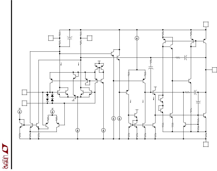
Rail-to-Rail Input
The LT1677 has the lowest voltage noise, offset voltage and highest gain when compared to any rail-to-rail op amp. The input common mode range for the LT1677 can exceed the supplies by at least 100mV. As the common mode voltage approaches the positive rail (+VS – 0.7V), the tail current for the input pair (Q1, Q2) is reduced, which prevents the input pair from saturating (refer to the Simplified Schematic). The voltage drop across the load resistors RC1, RC2 is reduced to less than 200mV, degrading the slew rate, bandwidth, voltage noise, offset voltage and input bias current (the cancellation is shut off).
When the input common mode range goes below 1.5V above the negative rail, the NPN input pair (Q1, Q2) shuts off and the PNP input pair (Q8, Q9) turns on. The offset voltage, input bias current, voltage noise and bandwidth are also degraded. The graph of Offset Voltage Shift vs Common Mode shows where the knees occur by displaying the change in offset voltage. The change-over points are temperature dependent, see the graph Common Mode Range vs Temperature.
Rail-to-Rail Output
The rail-to-rail output swing is achieved by using transistor collectors (Q28, Q29) instead of customary class A-B emitter followers for the output stage. Referring to the SimplifiedSchematic,theoutputNPNtransistor(Q29)sinks the current necessary to move the output in the negative direction. The change in Q29’s base emitter voltage is reflected directly to the gain node (collectors of Q20 and Q16). For large sinking currents, the delta VBE of Q29 can dominate the gain. Figure 9 shows the change in input voltage for a change in output voltage for different load resistors connected between the supplies. The gain is much higher for output voltages above ground (Q28 sources current) since the change in base emitter voltage of Q28 is attenuated by the gain in the PNP portion of the output stage. Therefore, for positive output swings (output sourcing current) there is hardly any change in input voltage for any load resistance. Highest gain and best linearity is achieved when the output is sourcing current, which is the case in singlesupplyoperationwhentheloadisgroundreferenced. Figure 10 shows gains for both sinking and sourcing load currents for a worst-case load of 600Ω.
INPUT VOLTAGE (50 V/DIV)
RL = 600
 RL = 1k
RL = 10k
– 15 – 10 – 5 0 |
5 10 15 |
TA = 25°C OUTPUT VOLTAGE (V)
VS = ±15V
RL CONNECTED TO 0V
MEASURED ON TEKTRONIX 577 CURVE TRACER
Figure 9. Voltage Gain Split Supply
(5 V/DIV) |
|
|
|
|
RL TO 5V |
|
|
|
|
|
|
INPUT VOLTAGE |
|
|
|
|
RL TO 0V |
|
|
|
|
|
|
0 |
1 |
2 |
3 |
4 |
5 |
TA = 25°C |
|
OUTPUT VOLTAGE (V) |
|
|
|
VS = 5V |
|
|
|
|
|
RL = 600Ω |
|
|
|
|
|
MEASURED ON TEKTRONIX 577 CURVE TRACER
Figure 10. Voltage Gain Single Supply
15
LT1677
TYPICAL APPLICATIOUS
Microvolt Comparator with Hysteresis
|
|
3V |
|
10M |
15k |
|
5% |
1% |
3 |
7 |
15k |
|
||
+ |
1 |
1% |
INPUT |
6 |
OUTPUT |
LT1677 |
2
–4
1677 TA03
POSITIVE FEEDBACK TO ONE OF THE NULLING TERMINALS CREATES APPROXIMATELY 5µV OF HYSTERESIS. OUTPUT CAN SINK 16mA
INPUT OFFSET VOLTAGE IS TYPICALLY CHANGED LESS THAN 5µV DUE TO THE FEEDBACK
|
|
3V Strain Gauge Amplifier |
|
||||
|
|
3V |
|
|
|
|
|
|
R9 |
R8 |
|
|
|
R7 |
|
R11 |
3.4Ω |
7.5Ω |
|
|
|
22.1Ω |
|
|
|
|
|
|
|
|
|
1k |
R* |
R* |
|
R2 |
R3 |
R5 |
|
|
|
|
|||||
|
|
|
|
5Ω |
5.49k |
698Ω |
|
R10 |
|
|
|
|
|
|
|
232Ω |
R* |
R* |
|
|
3V |
|
|
|
|
|
|
|
|
||
|
|
|
|
|
+ |
|
|
|
|
|
|
|
LT1677 |
|
VOUT |
|
|
|
|
|
– |
R* |
FOR TEMP |
|
|
|
|
|
|
|
|
|
|
|
|
R2 |
R4 |
R* |
COMPENSATION |
|
|
|
|
OF GAIN |
|||
|
|
|
|
5Ω |
5.49k |
||
|
|
|
|
|
|
||
|
*OMEGA SG-3/350LY11 |
|
R6 |
|
|||
|
350Ω , 1% |
|
|
|
|
||
|
|
|
|
22.1Ω |
|||
|
ALL OTHER RESISTORS 1% |
|
|||||
|
|
|
|
||||
|
AV = (2 • R* + R6)( |
R4 |
) 1000 |
1677 TA06 |
|||
|
|
|
|||||
|
|
R6 |
R2 + (R*/2) |
|
|
||
|
TRIM R11 FOR BRIDGE BALANCE |
|
|
||||
Precision High Side Current Sense
SOURCE
3V < VS < 36V
RIN
1k
RLINE |
2 |
|
– |
||
0.1Ω |
||
|
3
+
LOAD |
7 |
|
6 |
ZETEX |
LT1677 |
BC856B |
|
|
4 |
VOUT |
ROUT |
VOUT |
|
|
ROUT |
|
|
20k |
|
= RLINE |
|
|||
|
|
ILOAD |
|
RIN |
|
|
|
|
|
||||
= 2V/AMP
1677 TA07
16
LT1677
TYPICAL APPLICATIOUS
3V Super Electret Microphone Amplifier with DC Servo
1.5V |
|
|
|
|
|
|
|
|
|
1.5V |
2N3906 |
C1 |
|
|
|
|
|
|
|
C3 |
2N3906 |
|
|
7Hz POLE FOR SERVO |
|
|
||||||
10pF |
|
0.022 F |
|
|||||||
|
|
|
|
|
|
|
||||
|
|
|
|
|
|
|
|
|
|
R5 |
|
|
R1 |
16kHz |
|
R3 |
|
|
|
1.5V |
2k |
|
|
|
|
|
|
|
||||
|
|
1M |
ROLL OFF |
|
1M |
|
2 |
– |
7 |
|
|
|
|
|
|
|
|
|
|||
|
|
|
|
|
|
|
|
6 |
|
|
|
|
1.5V |
|
|
|
|
|
|
|
|
|
|
|
|
|
|
3 |
LT1677 |
|
||
2 |
– |
7 |
|
|
|
|
+ |
4 |
|
|
|
|
|
|
|
|
|||||
|
|
6 |
|
|
|
|
|
|
|
|
|
|
LT1677 |
|
|
|
|
|
–1.5V |
|
|
3 |
|
|
|
|
|
|
|
|
||
+ |
4 |
|
|
|
|
|
|
|
|
|
|
|
|
|
|
|
|
|
|
||
|
|
–1.5V |
|
|
|
|
|
R2 |
C2 |
|
|
|
|
|
|
|
|
80k |
100pF |
20kHz |
|
|
|
|
|
|
|
|
|
|||
|
|
|
|
|
|
|
|
|
|
|
|
|
|
|
C4 |
|
R4 |
|
|
1.5V |
ROLL OFF |
|
|
|
|
1 F |
|
|
|
|
||
|
|
|
|
|
8k |
2 |
|
|
|
|
PANASONIC |
|
|
|
|
|
– |
7 |
TO |
||
|
|
|
|
|
|
|||||
ELECTRET |
|
|
|
|
|
|
|
6 |
HEADPHONES |
|
CONDENSER |
|
|
|
|
|
|
|
|
|
|
|
|
|
|
|
|
|
LT1677 |
|
||
MICROPHONE |
|
|
|
|
|
|
3 |
+ |
|
|
WM-61 |
|
|
|
|
|
|
4 |
|
||
|
|
|
|
|
|
|
|
|||
(714) 373-7334 |
|
|
|
|
|
|
|
|
|
|
–1.5V |
|
|
|
|
|
|
|
|
–1.5V |
1677 TA05 |
17
18
RC1B |
RC2B |
R32 |
1k |
1k |
1.5k |
|
PAD |
C10 |
|
PAD |
|
|
200µA |
|
|
|
81pF |
|
|
|
|
|
|||
|
1 |
|
8 |
|
|
|
|
|
|
|
RC1A |
+ |
|
RC2A |
|
|
|
|
Q32 |
|
6k |
|
|
6k |
|
|
|
|
|
|
|
|
|
|
|
Q17 |
|
|
|
|
|
|
|
|
|
Q18 |
|
|
|
|
|
|
|
|
|
|
|
R2 |
|
|
|
100µA |
|
|
|
|
+ |
50Ω |
|
|
|
|
|
|
|
C2 |
|
||
|
|
|
|
|
Q4 |
Q7 |
|
||
|
|
|
|
|
|
80pF |
|
||
|
|
|
|
|
|
|
|
|
|
|
|
|
|
|
|
R19 |
R20 |
|
|
|
|
Q12 |
|
|
|
2k |
2k |
|
|
|
|
|
|
|
|
|
|
|
|
|
Q5 |
|
|
Q10 |
Q6 |
Q11 |
Q20 |
|
|
|
|
|
|
|
|
|
|||
–IN |
Q1A |
Q1B |
Q2A |
Q2B |
|
Q19 |
|
Q23 |
|
|
|
|
|
|
|
||||
D4 |
D1 |
Q3 |
|
|
|
|
|
|
|
D3 |
D2 |
|
|
|
|
|
160µA |
Q31 |
|
|
|
|
|
|
100µA |
|
|||
+IN |
|
|
|
|
|
|
|
|
|
|
|
|
|
|
|
|
|
|
|
IA |
|
|
IB |
|
|
|
|
|
|
|
Q30 |
|
|
|
|
|
|
|
|
|
|
||
|
|
|
R8 |
|
R9 |
|
|
Q22 |
|
|
|
|
|
|
|
50µA |
50µA |
|
|
|
|
||
|
|
|
200Ω |
200Ω |
|
|
|
|
|
|
|
Q13 |
Q21 |
Q24 |
Q8 |
|
Q9 |
|
Q15 |
Q14 |
Q16 |
Q25 |
R30 |
×2 |
|
|
|
|
|
2k |
|||||
|
|
|
|
|
IC |
ID |
|
|
|
|
|
R13 |
R21 |
R24 |
|
|
|
|
R15 |
R14 |
R16 |
R25 |
|
100Ω |
100Ω |
100Ω |
|
|
|
|
1k |
1k |
1k |
1k |
|
IA, IB = 0µA VCM > 1.5V ABOVE –VS |
|
IC = 200µA VCM < 0.7V BELOW +VS |
ID = 100µA VCM < 0.7V BELOW +VS |
|
|
|
|
|
|||
|
200µA VCM < 1.5V ABOVE –VS |
|
50µA VCM > 0.7V BELOW +VS |
0µA VCM > 0.7V BELOW +VS |
|
|
|
|
|
||
+VS |
R34
2k
Q34
Q28
 Q35
Q35
C1
R1 40pF
500Ω
+
OUT |
|
|
Q27 |
|
|
R3 |
C3 |
|
|
40pF |
|
|
|
100Ω |
|
|
|
|
+ |
|
|
|
|
C4 |
|
|
+ |
20pF |
|
|
|
|
|
|
R54 |
|
Q26 |
|
100Ω |
|
|
|
Q29 |
|
|
|
|
|
|
|
R23A |
|
R26 |
|
10k |
|
Q38 |
|
|
|
100Ω |
|
R23B |
|
|
|
||
|
|
10k |
|
|
|
|
R29 |
|
|
|
10Ω |
–VS
1677 SS
PLIFIEDWSI |
|
LT1677 |
|
||
ATICWSCHE |
|
|
|
|
|

LT1677
Dimensions in inches (millimeters) unless otherwise noted.
N8 Package
8-Lead PDIP (Narrow 0.300)
(LTC DWG # 05-08-1510)
|
|
|
|
|
|
|
|
|
|
|
|
|
|
|
|
|
|
|
|
|
|
|
|
|
|
|
|
|
|
|
0.400* |
|
|
|
|
|
|
|
|
|
|
|
|
|
|
|
|
|
|
|
|
|
|
|||||
|
|
|
|
|
|
|
|
|
|
|
|
|
|
|
|
|
|
|
|
|
|
|
|
|
|
|
|
|
|
|
|
|
|
|
|
|
|
|
|
|
|
|
|
|
|
|
|
|
|
|
|
|||||||
|
|
|
|
|
|
|
|
|
|
|
|
|
|
|
|
|
|
|
|
|
|
|
|
|
|
|
|
|
|
(10.160) |
|
|
|
|
|
|
|
|
|
|
|
|
|
|
|
|
|
|
|
|
|
|||||||
|
|
|
|
|
|
|
|
|
|
|
|
|
|
|
|
|
|
|
|
|
|
|
|
|
|
|
|
|
|
|
|
MAX |
|
|
|
|
|
|
|
|
|
|
|
|
|
|
|
|
|
|
|
|
||||||
|
|
|
|
|
|
|
|
|
|
|
|
|
|
|
|
|
|
|
|
|
|
|
|
|
|
|
|
|
|
|
|
|
|
|
|
|
|
|
|
|
|
|
|
|
|
|
|
|
|
|
|
|
||||||
|
|
|
|
|
|
|
|
|
|
|
|
|
|
|
|
|
|
|
|
|
8 |
|
|
7 |
|
|
|
|
|
6 |
|
|
|
|
5 |
|
|
|
|
|
|
|
|
|
|
|
|
|
|
|
||||||||
|
|
|
|
|
|
|
|
|
|
|
|
|
|
|
|
|
|
|
|
|
|
|
|
|
|
|
|
|
|
|
|
|
|
|
|
|
|
|
|
|
|
|
|
|
|
|
|
|
|
|
|
|
||||||
|
|
|
|
|
|
|
|
|
|
|
|
|
|
|
|
|
|
|
|
|
|
|
|
|
|
|
|
|
|
|
|
|
|
|
|
|
|
|
|
|
|
|
|
|
|
|
|
|
||||||||||
|
|
|
|
|
|
|
|
|
|
|
|
0.255 ± 0.015* |
|
|
|
|
|
|
|
|
|
|
|
|
|
|
|
|
|
|
|
|
|
|
|
|
|
|
|
|
|
|
|
|
|
|
|
|
||||||||||
|
|
|
|
|
|
|
|
|
|
|
|
|
|
|
|
|
|
|
|
|
|
|
|
|
|
|
|
|
|
|
|
|
|
|
|
|
|
|
|
|
|
|
|
|
|
|
|
|
|
|
|
|
||||||
|
|
|
|
|
|
|
|
|
|
|
(6.477 ± 0.381) |
|
|
|
|
|
|
|
|
|
|
|
|
|
|
|
|
|
|
|
|
|
|
|
|
|
|
|
|
|
|
|
|
|
|
|
|
|||||||||||
|
|
|
|
|
|
|
|
|
|
|
|
|
|
|
|
|
|
|
|
|
|
|
|
|
|
|
|
|
|
|
|
|
|
|
|
|
|
|
|
|
|
|
|
|
|
|
|
|
|
|
|
|||||||
|
|
|
|
|
|
|
|
|
|
|
|
|
|
|
|
|
|
|
|
|
|
|
|
|
|
|
|
|
|
|
|
|
|
|
|
|
|
|
|
|
|
|
|
|
|
|
|
|
|
|
|
|
|
|
|
|
|
|
|
|
|
|
|
|
|
|
|
|
|
|
|
|
|
|
|
|
|
|
|
|
|
|
|
|
|
|
|
|
|
|
|
|
|
|
|
|
|
|
|
|
|
|
|
|
|
|
|
|
|
|
|
|
|
|
|
|
|
|
|
|
|
|
|
|
|
|
|
|
|
|
|
|
|
|
|
|
|
|
|
|
|
|
|
|
|
|
|
|
|
|
|
|
|
|
|
|
|
|
|
|
|
|
|
|
|
|
|
|
|
|
|
|
|
|
|
|
|
|
|
|
|
|
|
|
|
|
|
|
|
|
|
|
|
|
|
|
|
|
|
|
|
|
|
1 |
|
|
2 |
|
|
|
|
|
3 |
|
|
|
4 |
|
|
|
|
|
|
|
|
|
|
|
|
|
|
|
|||
|
|
|
|
0.300 – 0.325 |
|
|
|
|
|
|
|
|
|
|
|
|
|
|
0.045 – 0.065 |
|
|
|
|
|
|
|
|
|
0.130 ± 0.005 |
|
|
|
||||||||||||||||||||||||||
|
|
|
|
|
|
|
|
|
|
|
|
|
|
|
|
|
|
|
|
|
|
|
|
|||||||||||||||||||||||||||||||||||
|
|
|
|
|
|
|
|
|
|
|
|
|
|
|
|
|
|
|
|
|
|
|
|
|||||||||||||||||||||||||||||||||||
|
|
|
|
|
|
|
|
|
|
|
|
|
|
|
|
|
|
|
|
|
|
|
|
|
|
|
|
|
|
|
|
|
|
|
|
|
|
|
|
|
|
|
|
|
|
|
|
|
|
|
|
|
|
|
||||
|
|
|
|
(7.620 – 8.255) |
|
|
|
|
|
|
|
|
|
|
|
|
|
|
|
(1.143 – 1.651) |
|
|
|
|
|
|
|
|
|
|
|
(3.302 ± 0.127) |
|
|
||||||||||||||||||||||||
|
|
|
|
|
|
|
|
|
|
|
|
|
|
|
|
|
|
|
|
|
|
|
|
|
|
|||||||||||||||||||||||||||||||||
|
|
|
|
|
|
|
|
|
|
|
|
|
|
|
|
|
|
|
|
|
|
|
|
|
|
|
|
|
|
|
|
|
|
|
|
|
|
|
|
|
|
|
|
|
|
|
|
|
|
|
|
|
|
|
|
|
|
|
|
|
|
|
|
|
|
|
|
|
|
|
|
|
|
|
|
|
|
|
|
|
|
|
|
|
|
|
|
|
|
|
|
|
|
|
|
|
|
|
|
|
|
|
|
|
|
|
|
|
|
|
|
|
|
|
|
|
|
|
|
|
|
|
|
|
|
|
|
|
|
|
|
|
|
|
|
|
|
|
|
|
|
|
|
|
|
|
|
|
|
|
|
|
|
|
|
|
|
|
|
|
|
|
|
|
|
|
|
|
|
|
|
|
|
|
|
|
|
|
|
|
|
|
|
|
|
|
|
0.065 |
|
|
|
|
|
|
|
|
|
|
|
|
|
|
|
|
|
|
|
|
|
|
|
|
|
|
|
|
|
|
|
|
|
|
|
|
|
|
|
|
|
|
|
||||
|
|
|
|
|
|
|
|
|
|
|
|
|
|
|
|
|
|
|
|
|
|
|
|
|
|
|
|
|
|
|
|
|
|
|
|
|
|
|
|
|
|
|
|
|
|
|
|
|
|
|
|
|
|
|||||
|
|
|
|
|
|
|
|
|
|
|
|
|
|
|
|
|
|
|
|
|
|
|
|
|
|
|
|
|
|
|
|
|
|
|
|
|
|
|
|
|
|
|
|
|
|
|
|
|
|
|
|
|
|
|||||
|
|
|
|
|
|
|
|
|
|
|
|
|
|
|
|
|
|
|
|
|
|
|
|
|
|
|
|
|
|
|
|
|
|
|
|
|
|
|
|
|
|
|
|
|
|
|
|
|
|
|
|
|
|
|||||
|
|
|
|
|
|
|
|
|
|
|
|
|
(1.651) |
|
|
|
|
|
|
|
|
|
|
|
|
|
|
|
|
|
|
|
|
|
|
|
|
|
|
|
|
|
|
|
|
|
|
|
|
|
|
|
|
|
|
|
||
|
|
|
|
|
|
|
|
|
|
|
|
|
|
|
|
|
|
|
|
|
|
|
|
|
|
|
|
|
|
|
|
|
|
|
|
|
|
|
|
|
|
|
|
|
|
|
|
|
|
|
|
|
|
|
|
|||
|
|
|
|
0.009 – 0.015 |
|
|
TYP |
|
|
|
|
|
|
|
|
|
|
|
|
|
|
|
|
|
|
|
|
|
|
|
|
|
|
|
|
|
||||||||||||||||||||||
|
|
|
|
|
|
|
|
|
|
|
|
|
|
|
|
|
|
|
0.125 |
|
|
|
|
|
|
|
||||||||||||||||||||||||||||||||
|
|
|
|
(0.229 – 0.381) |
|
|
|
|
|
|
|
|
|
|
|
|
|
|
|
|
|
|
|
|
|
|
|
|
|
|
|
|
|
|
|
|
|
|
|
|
|
|
|
|
|
|
|
|||||||||||
|
|
|
|
|
|
|
|
|
|
|
|
|
|
|
|
|
|
|
|
|
|
|
|
|
|
|
|
|
|
|
|
|
|
|
|
|
|
|
|
|
|
|
|
|
|
|
0.020 |
|
||||||||||
|
|
+0.035 |
|
|
|
|
|
|
|
|
|
|
|
|
|
|
|
|
|
|
|
|
|
|
|
|
|
|
|
|
|
|
|
|
|
|
|
|
|
|
|
(3.175) |
|
|||||||||||||||
|
|
|
|
|
|
|
|
|
|
|
|
|
|
|
|
|
|
|
|
|
|
|
|
|
|
|
|
|
|
|
|
|
|
|
|
|
|
|
|
|
|
|
|
|
MIN |
(0.508) |
||||||||||||
|
|
|
|
0.325 –0.015 |
|
|
|
0.100 |
|
|
|
|
|
|
|
|
|
|
|
|
|
|
|
0.018 ± 0.003 |
|
|
MIN |
|||||||||||||||||||||||||||||||
|
|
+0.889 |
|
|
|
|
(2.54) |
|
|
|
|
|
|
|
|
|
|
|
|
|
|
|
|
|
|
|
|
|
|
|
|
|
|
|
|
|
|
|
|
|
||||||||||||||||||
|
|
|
|
(8.255 –0.381) |
|
|
|
|
|
|
|
|
|
|
|
|
|
(0.457 ± 0.076) |
|
N8 1098 |
||||||||||||||||||||||||||||||||||||||
|
|
|
|
|
|
|
|
|
|
|
|
|
|
|
BSC |
|
|
|
|
|
|
|
|
|
|
|||||||||||||||||||||||||||||||||
|
|
|
|
|
|
|
|
|
|
|
|
|
|
|
|
|
|
|
|
|
|
|
|
|
|
|
|
|
|
|
|
|
|
|
|
|
|
|
|
|
|
|
|
|
|
|
|
|
|
|
||||||||
*THESE DIMENSIONS DO NOT INCLUDE MOLD FLASH OR PROTRUSIONS. MOLD FLASH OR PROTRUSIONS SHALL NOT EXCEED 0.010 INCH (0.254mm)
S8 Package
8-Lead Plastic Small Outline (Narrow 0.150)
(LTC DWG # 05-08-1610)
|
|
|
|
|
|
|
|
|
|
|
|
|
|
|
|
|
|
0.189 – 0.197* |
|
|
|
|
|
|
|
|||||
|
|
|
|
|
|
|
|
|
|
|
|
|
|
|
|
|
|
|
|
|
|
|
|
|||||||
|
|
|
|
|
|
|
|
|
|
|
|
|
|
|
|
|
|
(4.801 – 5.004) |
|
|
|
|
|
|
|
|
||||
|
|
|
|
|
|
|
|
|
|
|
8 |
7 |
6 |
|
|
5 |
|
|
|
|
|
|
||||||||
|
|
|
|
|
|
|
|
|
|
|
|
|
|
|
|
|
|
|
|
|
|
|
|
|
|
|
|
|
|
|
|
|
|
|
|
|
|
|
|
|
|
|
|
|
|
|
|
|
|
|
|
|
|
|
|
|
|
|
|
|
|
|
|
|
|
|
|
|
|
|
|
|
|
|
|
|
|
|
|
|
|
|
|
|
|
|
|
|
|
|
|
|
|
|
|
|
|
|
|
|
|
|
|
|
|
|
|
|
|
|
|
|
|
|
|
|
|
|
|||||
|
|
|
|
|
|
|
|
|
|
|
|
|
|
|
|
|
|
|
|
|
|
|
|
|
|
|
|
|
|
|
|
|
|
|
|
|
|
|
|
|
0.228 – 0.244 |
|
|
|
|
|
|
|
|
|
|
|
|
0.150 – 0.157** |
|||||||
|
|
|
|
|
|
|
|
|
|
(5.791 – 6.197) |
|
|
|
|
|
|
|
|
|
|
|
|
|
(3.810 – 3.988) |
||||||
|
|
|
|
|
|
|
|
|
|
|
|
|
|
|
|
|
|
|
|
|
|
|
|
|
|
|||||
|
|
|
|
|
|
|
|
|
|
|
|
|
|
|
|
|
|
|
|
|
|
|
|
|
|
|
|
|
|
|
|
|
|
|
|
|
|
|
|
|
|
|
|
|
|
|
|
|
|
|
|
|
|
|
|
|
|
|
|
|
|
|
|
|
|
|
|
|
|
|
|
|
|
|
|
|
|
|
|
|
|
|
|
|
|
|
|
|||||
|
|
|
|
|
|
|
|
|
|
|
|
|
|
|
|
|
|
|
|
|
|
|
|
|
|
|
|
|
|
|
|
|
|
|
|
|
1 |
2 |
3 |
|
|
4 |
|
|
|
|
|
|
|||||||||||||
|
0.010 – 0.020 |
× 45° |
|
|
|
|
|
|
|
|
0.053 – 0.069 |
|
|
|
|
|
|
|
|
|
|
|
|
|
|
|||||
|
(0.254 – 0.508) |
|
|
|
|
|
|
|
|
|
|
|
|
|
|
|
|
|
|
|||||||||||
|
|
|
|
|
|
|
|
|
|
(1.346 – 1.752) |
|
|
|
|
|
|
|
|
|
|
|
|
|
|
||||||
|
|
|
|
|
|
|
|
|
|
|
|
|
|
|
|
|
|
|
|
|
|
0.004 – 0.010 |
||||||||
0.008 – 0.010 |
|
|
|
|
|
|
|
|
|
|
|
|
|
|
|
|
|
|
|
|
|
|
|
|
|
|
||||
(0.203 – 0.254) |
|
|
|
|
|
0°– 8 |
°TYP |
|
|
|
|
|
|
|
|
|
|
|
|
|
(0.101 – 0.254) |
|||||||||
|
|
|
|
|
|
|
|
|
|
|
|
|
|
|
|
|
|
|
|
|
|
|
|
|
|
|
|
|
|
|
|
|
|
|
|
|
|
|
|
|
|
|
|
|
|
|
|
|
|
|
|
|
|
|
|
|
|
|
|
|
|
|
|
|
|
|
|
|
|
|
|
|
|
|
|
|
|
|
|
|
|
|
|
|
|
|
|
|
|
|
|
|
|
|
|
|
|
|
|
|
|
|
|
|
|
|
|
|
|
|
|
|
|
|
|
|
|
|
|
|
|
|
|
0.016 – 0.050
(0.406 – 1.270)
0.014 – 0.019
(0.355 – 0.483) TYP
*DIMENSION DOES NOT INCLUDE MOLD FLASH. MOLD FLASH SHALL NOT EXCEED 0.006" (0.152mm) PER SIDE
**DIMENSION DOES NOT INCLUDE INTERLEAD FLASH. INTERLEAD FLASH SHALL NOT EXCEED 0.010" (0.254mm) PER SIDE
0.050
(1.270) BSC
SO8 1298
Information furnished by Linear Technology Corporation is believed to be accurate and reliable. |
19 |
However, no responsibility is assumed for its use. Linear Technology Corporation makes no represen- |
|
tation that the interconnection of its circuits as described herein will not infringe on existing patent rights. |

LT1677
TYPICAL APPLICATIOU
This 2-wire remote Geophone preamp operates on a current-loop principle and so has good noise immunity. Quiescent current is ≈10mA for a VOUT of 2.5V. Excitation will cause AC currents about this point of ~±4mA for a VOUT of ~±1V max. The op amp is configured for a voltage
gain of ~107. Components R5 and Q1 convert the voltage into a current for transmission back to R10, which converts it into a voltage again. The LM334 and 2N3904 are not temperature compensated so the DC output contains temperature information.
2-Wire Remote Geophone Preamp
R9
20Ω
LINEAR |
V + |
|
TECHNOLOGY |
R |
|
LM334Z |
V – |
R8 |
6mA |
||
|
|
11Ω |
3V |
|
|
|
|
|
|
|
|
|
Q1 |
12V |
|
R6 |
|
|
|
|
|
|
R2 |
2N3904 |
|
|
|
|
|
|
|
|
|
|
|
|||
C |
|
+ |
|
|
|
|
|
|
|
||
R |
4.99k |
C3 |
|
R4 |
|
|
100k |
|
|
||
LT1431CZ |
|
|
|
14k |
|
|
|
|
|
||
A |
|
R7 |
|
220µF |
|
|
|
|
|
R5 |
VOUT |
|
|
|
|
R1 |
|
|
|
||||
|
|
24.9k |
|
|
|
|
|
|
243Ω |
||
|
|
|
|
|
365Ω |
2 |
|
C2 |
2.5V ±1V |
||
|
|
|
|
|
|
|
|
||||
|
|
|
|
|
|
|
7 |
|
R10 |
||
|
|
|
|
GEOSPACE |
– |
|
– |
0.1µF |
|
||
|
|
|
|
|
|
|
250Ω |
||||
|
|
|
|
GS-20DX |
|
|
|
LT1677 |
6 |
|
|
|
|
|
|
RL = 630Ω |
+ |
|
|
|
|
|
|
|
|
|
|
|
3 |
|
|
|
|
||
|
|
|
|
GEOPHONE |
|
4 |
|
|
|
||
|
www.geospacecorp.com/default.htm |
|
|
+ |
|
|
|
||||
|
|
R3 |
|
|
|
C4 |
|
||||
|
|
|
|
(713) 939-7093 |
|
|
|
|
|
||
|
|
|
|
|
|
16.2k |
|
|
|
1000pF |
|
1677 TA04
AV = R2 + R3||R4 107
R1 + RL
RELATED PARTS
PART NUMBER |
DESCRIPTION |
COMMENTS |
||||||||||||||
|
|
|
|
|
|
|
|
|
|
|
|
|
|
|
|
|
LT1028/LT1128 |
Ultralow Noise Precision Op Amps |
Lowest Noise 0.85nV/√ |
|
|
|
|
||||||||||
Hz |
||||||||||||||||
LT1115 |
Ultralow Noise, Low distortion Audio Op Amp |
0.002% THD, Max Noise 1.2nV/√ |
|
|
||||||||||||
Hz |
||||||||||||||||
LT1124/LT1125 |
Dual/Quad Low Noise, High Speed Precision Op Amps |
Similar to LT1007 |
||||||||||||||
|
|
|
|
|
|
|
|
|
|
|
|
|
|
|
|
|
LT1126/LT1127 |
Dual/Quad Decompensated Low Noise, High Speed Precision Op Amps |
Similar to LT1037 |
||||||||||||||
|
|
|
|
|
|
|
|
|
|
|
|
|
|
|
|
|
LT1226 |
Low Noise, Very High Speed Op Amp |
1GHz, 2.6nV/√ |
|
Gain of 25 Stable |
||||||||||||
Hz, |
||||||||||||||||
LT1498/LT1499 |
10MHz, 5V/ s, Dual/Quad Rail-to-Rail Input and Output Op Amps |
Precision C-LoadTM Stable |
||||||||||||||
LT1792 |
Low Noise, Precision JFET Input Op Amp |
4.2nV/√ |
|
|
10fA/√ |
|
|
|||||||||
Hz, |
Hz |
|||||||||||||||
LT1793 |
Low Noise, Picoampere Bias Current Op Amp |
6nV/√ |
|
1fA/√ |
|
|
IB = 10pA Max |
|||||||||
Hz, |
Hz, |
|||||||||||||||
LT1806 |
Low Noise, 325MHz Rail-to-Rail Input and Output Op Amp |
3.5nV/√ |
|
|
||||||||||||
Hz |
||||||||||||||||
LT1881/LT1882 |
Dual/Quad Rail-to-Rail Output Picoamp Input Precision Op Amps |
CLOAD to 1000pF, IB = 200pA Max |
||||||||||||||
LT1884/LT1885 |
Dual/Quad Rail-to-Rail Output Picoamp Input Precision Op Amps |
2.2MHz Bandwidth, 1.2V/ s SR |
||||||||||||||
|
|
|
|
|
|
|
|
|
|
|
|
|
|
|
|
|
C-Load is a trademark of Linear Technology Corporation.
20 |
Linear Technology Corporation |
1630 McCarthy Blvd., Milpitas, CA 95035-7417 |
1677f LT/TP 0800 4K • PRINTED IN USA
(408)432-1900● FAX:(408)434-0507 ● www.linear-tech.com |
LINEAR TECHNOLOGY CORPORATION 2000 |