

FEATURES
n Gain Bandwidth Product: 720MHz n –3dB Frequency (AV = 1): 400MHz n Low Quiescent Current: 3.5mA Max n High Slew Rate: 280V/µs
n Input Common Mode Range Includes Both Rails n Output Swings Rail-to-Rail
n Low Broadband Voltage Noise: 2.75nV/√HZ n Power-Down Mode: 42μA
n Fast Output Recovery
n Supply Voltage Range: 2.5V to 5.25V n Input Offset Voltage: 350µV Max
n Large Output Current: 90mA n CMRR: 105dB
n Open Loop Gain: 60V/mV
n Operating Temperature Range: –40°C to 125°C n Single in 6-Pin TSOT-23
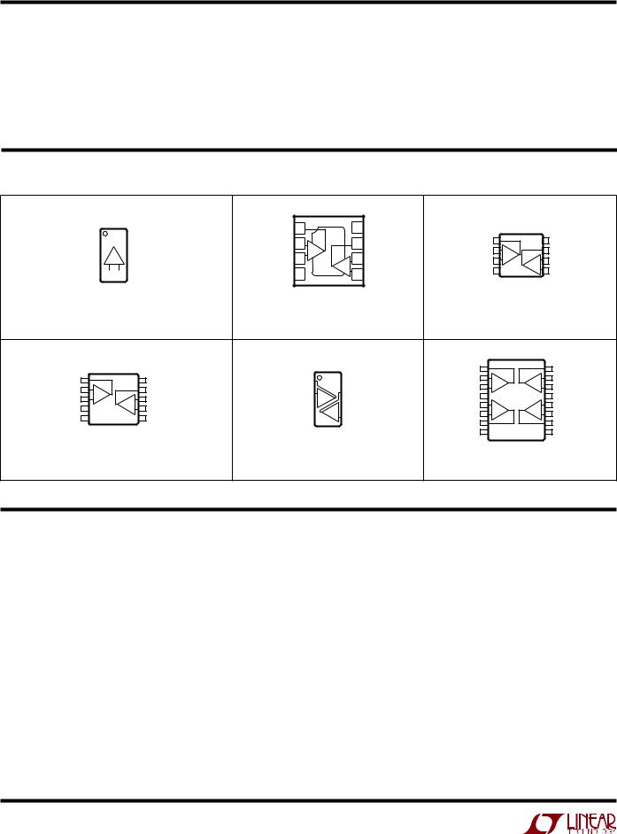
n Dual in MS8, 2mm × 2mm DFN, 8-Pin TS0T-23, MS10 n Quad in MS16
APPLICATIONS
n Low Voltage, High Frequency Signal Processing n Driving A/D Converters
n Rail-to-Rail Buffer Amplifiers n Active Filters
n Battery Powered Equipment
720MHz, 3.5mA Power Efficient Rail-to-Rail I/O Op Amps
DESCRIPTION
TheLTC®6252/LTC6253/LTC6254are single/dual/quad low power, high speed unity gain stable rail-to-rail input/output operational amplifiers. On only 3.5mA of supply current they feature a 720MHz gain-bandwidth product, 280V/µs slew rate and a low 2.75nV/√HZ of input-referred noise. The combination of high bandwidth, high slew rate, low power consumption and low broadband noise makes the LTC6252 family unique among rail-to-rail input/output op amps with similar supply currents. They are ideal for lower supply voltage high speed signal conditioning systems.
The LTC6252 family maintains high efficiency performance from supply voltage levels of 2.5V to 5.25V and is fully specified at supplies of 2.7V and 5.0V.
Forapplicationsthatrequirepower-down,theLTC6252and the LTC6253 in MS10 offer a shutdown pin which disables the amplifier and reduces current consumption to 42µA.
The LTC6252 family can be used as a plug-in replacement for many commercially available op amps to reduce power or to improve input/output range and performance.
L, LT, LTC, LTM, Linear Technology and the Linear logo are registered trademarks of Linear Technology Corporation. All other trademarks are the property of their respective owners.
TYPICAL APPLICATION
5V Single-Supply 16-Bit ADC Driver
5V |
5V |
1.8V TO 5V |
VIN |
+ |
|
|
|
10µF |
0.1µF |
10µF |
0.1µF |
|
4.7µF |
|
|
27.4mV TO |
½ LTC6253 |
|
|
|
|
|
|
|||||
(3.5V + 27.4mV) |
|
|
|
|
|
|
|
|
|
|
|
|
|
– |
|
|
|
|
AVP |
|
DVP |
|
OVP |
PARALLEL |
|
|
|
|
|
|
|
|
|
|
||||
|
|
|
|
|
|
|
|
|
|
|
|
|
|
143Ω |
2.5k |
2.5k |
249 |
100 |
IN+ |
|
|
|
|
OR |
16 BIT |
|
|
|
|
|
|
|
SERIAL |
|||||
|
|
|
|
|
|
|
|
|
|
|
INTERFACE |
|
|
845Ω |
|
|
3900pF |
|
|
|
LTC2393-16 |
|
SER/PAR |
|
|
|
|
|
– |
|
|
|
|
|
|
|
|
|
|
|
|
249 |
100 |
|
|
|
|
|
BYTESWAP |
|
|
|
|
|
½ LTC6253 |
IN– |
|
|
|
|
OB/2C |
|
||
|
|
|
|
|
|
|
|
|
|
|||
|
|
|
|
|
|
|
|
|
CS |
|
||
|
|
|
+ |
|
|
|
|
|
|
|
|
|
|
|
|
|
|
REFIN |
|
CNVST RESET |
|
RD |
|
||
|
|
|
|
|
|
VCM |
REFOUT |
PD |
GND OGND |
BUSY |
|
|
|
|
|
|
|
|
|
|
|
|
|
625234 TA01 |
|
|
|
|
~2.08V |
|
|
10µF |
1µF |
|
|
|
|
|
|
|
|
|
|
|
|
|
SAMPLE CLOCK |
|
|
||
LTC6253 Driving LTC2393-16
16-Bit ADC 5V Single-Supply
Performance
|
0 |
|
|
|
|
|
|
|
|
|
|
|
|
fS |
= 1Msps |
|
|
|
–20 |
|
|
|
F1 |
= 20.111kHz |
|
|
|
|
|
|
|
|
|||
|
|
|
|
|
F1 AMPLITUDE |
|
|
|
|
–40 |
|
|
|
|
= –1.032dBFS |
|
|
(dBFS) |
|
|
|
SNR = 93.28dB |
|
|
||
|
|
|
|
|
|
|||
|
|
|
|
SINAD = 92.53dB |
|
|||
|
–60 |
|
|
|
THD = –100.50dB |
|
||
AMPLITUDE |
|
|
|
SFDR = 104.7dB |
|
|
||
–80 |
|
|
|
|
|
|||
|
|
|
F2 |
= –106.39dBc |
|
|||
|
|
|
|
|
||||
|
|
|
|
|
|
|||
|
–100 |
|
|
|
F3 |
= –104.70dBc |
|
|
|
|
|
|
F4 |
= –114.13dBc |
|
||
|
|
|
|
|
|
|||
|
–120 |
|
|
|
F5 |
= –105.48dBc |
|
|
|
|
|
|
|
|
|
|
|
|
–140 |
|
|
|
|
|
|
|
|
|
|
|
|
|
|
|
|
|
|
|
|
|
|
|
|
|
|
–160 |
|
|
|
|
|
|
|
|
0 |
100 |
200 |
300 |
400 |
500 |
||
FREQUENCY (kHz)
624678 TA01b
625234fc
1
LTC6252/LTC6253/LTC6254
ABSOLUTE MAXIMUM RATINGS (Note 1)
Total Supply Voltage (V+ to V–)................................ |
5.5V |
Input Current (+IN, –IN, SHDN) (Note 2).............. |
±10mA |
Output Current (Note 3)...................................... |
±100mA |
Operating Temperature Range (Note 4).. |
–40°C to 125°C |
Specified Temperature Range (Note 5)... |
–40°C to 125°C |
Storage Temperature Range................... |
–65°C to 150°C |
Junction Temperature............................................ |
150°C |
Lead Temperature (Soldering, 10 sec) |
|
MSOP, TSOT Packages Only.............................. |
300°C |
PIN CONFIGURATION
|
|
TOP VIEW |
|
||||||
OUT 1 |
|
|
|
|
|
|
|
|
6 V+ |
V– 2 |
|
+ |
|
– |
|
5 SHDN |
|||
|
|
|
|||||||
+IN 3 |
|
|
|
|
4 –IN |
||||
|
|
|
|
|
|
|
|
||
S6 PACKAGE
6-LEAD PLASTIC TSOT-23
TJMAX = 150°C, θJA = 192°C/W (NOTE 9)
|
|
TOP VIEW |
|
|
|
OUT A |
1 |
|
|
10 |
V+ |
–IN A |
2 |
– |
|
9 |
OUT B |
+IN A |
3 |
+ |
– |
8 |
–IN B |
V– |
4 |
|
+ |
7 |
+IN B |
SHDNA |
5 |
|
|
6 |
SHDNB |
|
|
MS PACKAGE |
|
|
|
|
10-LEAD PLASTIC MSOP |
|
|||
TJMAX = 150°C, θJA = 160°C/W (NOTE 9)
TOP VIEW
OUT A |
1 |
|
|
|
8 |
V+ |
–IN A |
2 |
– |
|
|
7 |
OUT B |
+IN A |
3 |
+ |
|
– |
6 |
–IN B |
V– |
|
|
9 |
|
|
|
4 |
|
+ |
5 |
+IN B |
DC PACKAGE
8-LEAD (2mm × 2mm) PLASTIC DFN
TJMAX = 125°C, θJA = 102°C/W (NOTE 9)
EXPOSED PAD (PIN 9) IS V–, MUST BE SOLDERED TO PCB
|
|
TOP VIEW |
|
||||
OUT A 1 |
|
|
|
|
|
|
8 V+ |
|
|
|
|
|
|
||
–IN A 2 |
|
– |
|
|
|
7 OUT B |
|
|
|
|
|
||||
|
|
||||||
+IN A 3 |
|
|
|
|
|
6 –IN B |
|
V– 4 |
|
|
|
|
– |
|
5 +IN B |
|
|
|
+ |
|
|||
|
|
|
|||||
TS8 PACKAGE
8-LEAD PLASTIC TSOT-23
TJMAX = 150°C, θJA = 195°C/W (NOTE 9)
|
|
TOP VIEW |
|
|
|
OUT A |
1 |
|
|
8 |
V+ |
–IN A |
2 |
– |
|
7 |
OUT B |
+IN A |
3 |
+ |
– |
6 |
–IN B |
V– |
4 |
|
+ |
5 |
+IN B |
MS8 PACKAGE
8-LEAD PLASTIC MSOP
TJMAX = 150°C, θJA = 163°C/W (NOTE 9)
|
|
|
TOP VIEW |
|
|
OUT A |
1 |
|
|
16 |
OUT D |
–IN A |
2 |
– |
– |
15 |
–IN D |
+IN A |
3 |
+ |
+ |
14 |
+IN D |
V+ |
4 |
|
+ |
13 |
V– |
+IN B |
5 |
+ |
12 |
+IN C |
|
–IN B |
6 |
– |
– |
11 |
–IN C |
OUT B |
7 |
|
|
10 |
OUT C |
|
8 |
|
|
9 |
|
|
|
MS PACKAGE |
|
|
|
|
16-LEAD PLASTIC MSOP |
|
|||
TJMAX = 150°C, θJA = 125°C/W (NOTE 9)
ORDER INFORMATION
LEAD FREE FINISH |
TAPE AND REEL |
PART MARKING* |
PACKAGE DESCRIPTION |
SPECIFIED TEMPERATURE RANGE |
|
|
|
|
|
LTC6252CS6#TRMPBF |
LTC6252CS6#TRPBF |
LTFRW |
6-Lead Plastic TSOT-23 |
0°C to 70°C |
|
|
|
|
|
LTC6252IS6#TRMPBF |
LTC6252IS6#TRPBF |
LTFRW |
6-Lead Plastic TSOT-23 |
–40°C to 85°C |
|
|
|
|
|
LTC6252HS6#TRMPBF |
LTC6252HS6#TRPBF |
LTFRW |
6-Lead Plastic TSOT-23 |
–40°C to 125°C |
|
|
|
|
|
LTC6253CDC#TRMPBF |
LTC6253CDC#TRPBF |
LFRZ |
8-Lead (2mm × 2mm) Plastic DFN |
0°C to 70°C |
|
|
|
|
|
LTC6253IDC#TRMPBF |
LTC6253IDC#TRPBF |
LFRZ |
8-Lead (2mm × 2mm) Plastic DFN |
–40°C to 85°C |
|
|
|
|
|
LTC6253CMS8#PBF |
LTC6253CMS8#TRPBF |
LTFRX |
8-Lead Plastic MSOP |
0°C to 70°C |
|
|
|
|
|
LTC6253IMS8#PBF |
LTC6253IMS8#TRPBF |
LTFRX |
8-Lead Plastic MSOP |
–40°C to 85°C |
|
|
|
|
|
LTC6253HMS8#PBF |
LTC6253HMS8#TRPBF |
LTFRX |
8-Lead Plastic MSOP |
–40°C to 125°C |
|
|
|
|
|
LTC6253CTS8#TRMPBF |
LTC6253CTS8#TRPBF |
LTFRY |
8-Lead Plastic TSOT-23 |
0°C to 70°C |
|
|
|
|
|
LTC6253ITS8#TRMPBF |
LTC6253ITS8#TRPBF |
LTFRY |
8-Lead Plastic TSOT-23 |
–40°C to 85°C |
|
|
|
|
|
LTC6253HTS8#TRMPBF |
LTC6253HTS8#TRPBF |
LTFRY |
8-Lead Plastic TSOT-23 |
–40°C to 125°C |
|
|
|
|
|
|
|
|
|
625234fc |
2

LTC6252/LTC6253/LTC6254
ORDER INFORMATION
LEAD FREE FINISH |
TAPE AND REEL |
PART MARKING* |
PACKAGE DESCRIPTION |
SPECIFIED TEMPERATURE RANGE |
|
|
|
|
|
LTC6253CMS#PBF |
LTC6253CMS#TRPBF |
LTFSB |
10-Lead Plastic MSOP |
0°C to 70°C |
|
|
|
|
|
LTC6253IMS#PBF |
LTC6253IMS#TRPBF |
LTFSB |
10-Lead Plastic MSOP |
–40°C to 85°C |
|
|
|
|
|
LTC6254CMS#PBF |
LTC6254CMS#TRPBF |
6254 |
16-Lead Plastic MSOP |
0°C to 70°C |
|
|
|
|
|
LTC6254IMS#PBF |
LTC6254IMS#TRPBF |
6254 |
16-Lead Plastic MSOP |
–40°C to 85°C |
|
|
|
|
|
LTC6254HMS#PBF |
LTC6254HMS#TRPBF |
6254 |
16-Lead Plastic MSOP |
–40°C to 125°C |
|
|
|
|
|
TRM = 500 pieces. *Temperature grades are identified by a label on the shipping container.
Consult LTC Marketing for parts specified with wider operating temperature ranges.
Consult LTC Marketing for information on lead based finish parts.
For more information on lead free part marking, go to: http://www.linear.com/leadfree/
For more information on tape and reel specifications, go to: http://www.linear.com/tapeandreel/
ELECTRICAL CHARACTERISTICS (VS = 5V) The l denotes the specifications which apply across the specified temperature range, otherwise specifications are at TA = 25°C. For each amplifier VS = 5V, 0V; VSHDN = 2V; VCM = VOUT = 2.5V, unless otherwise noted.
SYMBOL |
PARAMETER |
CONDITIONS |
MIN |
TYP |
MAX |
UNITS |
|||
|
|
|
|
|
|
|
|
||
VOS |
Input Offset Voltage |
VCM = Half Supply |
|
–350 |
50 |
350 |
µV |
||
|
|
|
|
|
l |
–1000 |
|
1000 |
µV |
|
|
V |
CM |
= V+ – 0.5V, NPN Mode |
|
–2.2 |
0.1 |
2.2 |
mV |
|
|
|
|
|
–3.3 |
|
–3.3 |
mV |
|
|
|
|
|
|
l |
|
|||
VOS |
Input Offset Voltage Match |
VCM = Half Supply |
|
–350 |
50 |
350 |
µV |
||
|
(Channel-to-Channel) (Note 8) |
|
|
|
l |
–550 |
|
550 |
µV |
|
|
V |
CM |
= V+ – 0.5V, NPN Mode |
|
–2.75 |
0.1 |
2.75 |
mV |
|
|
|
|
|
–4 |
|
4 |
mV |
|
|
|
|
|
|
l |
|
|||
VOS TC |
Input Offset Voltage Drift |
|
|
|
l |
|
–3.5 |
|
µV/°C |
|
|
|
|
|
|
|
|
||
IB |
Input Bias Current (Note 7) |
VCM = Half Supply |
|
–0.75 |
–0.1 |
0.75 |
µA |
||
|
|
|
|
|
l |
–1.15 |
|
1.15 |
µA |
|
|
V |
CM |
= V+ – 0.5V, NPN Mode |
|
0.8 |
1.4 |
3.0 |
µA |
|
|
|
|
|
0.4 |
|
5.0 |
µA |
|
|
|
|
|
|
l |
|
|||
IOS |
Input Offset Current |
VCM = Half Supply |
|
–0.5 |
–0.03 |
0.5 |
µA |
||
|
|
|
|
|
l |
–0.6 |
|
0.6 |
µA |
|
|
V |
CM |
= V+ – 0.5V, NPN Mode |
|
–0.5 |
–0.03 |
0.5 |
µA |
|
|
|
|
|
–0.6 |
|
0.6 |
µA |
|
|
|
|
|
|
l |
|
|||
en |
Input Noise Voltage Density |
f = 1MHz |
|
|
2.75 |
|
nV/√HZ |
||
|
Input 1/f Noise Voltage |
f = 0.1Hz to 10Hz |
|
|
2 |
|
µVP-P |
||
in |
Input Noise Current Density |
f = 1MHz |
|
|
4 |
|
pA/√HZ |
||
CIN |
Input Capacitance |
Differential Mode |
|
|
2.5 |
|
pF |
||
|
|
Common Mode |
|
|
0.8 |
|
pF |
||
RIN |
Input Resistance |
Differential Mode |
|
|
7.2 |
|
kΩ |
||
|
|
Common Mode |
|
|
3 |
|
MΩ |
||
AVOL |
Large Signal Voltage Gain |
RL = 1k to Half Supply (Note 10) |
|
35 |
60 |
|
V/mV |
||
|
|
|
|
|
l |
16 |
|
|
V/mV |
|
|
RL = 100Ω to Half Supply (Note 10) |
|
5 |
13 |
|
V/mV |
||
|
|
|
|
|
l |
2.4 |
|
|
V/mV |
CMRR |
Common Mode Rejection Ratio |
VCM = 0V to 3.5V |
|
85 |
105 |
|
dB |
||
|
|
|
|
|
l |
82 |
|
|
dB |
|
|
|
|
|
|
|
|
|
625234fc |
3

LTC6252/LTC6253/LTC6254
ELECTRICAL CHARACTERISTICS (VS = 5V) The l denotes the specifications which apply across the specified temperature range, otherwise specifications are at TA = 25°C. For each amplifier VS = 5V, 0V; VSHDN = 2V; VCM = VOUT = 2.5V, unless otherwise noted.
SYMBOL |
PARAMETER |
|
|
CONDITIONS |
MIN |
TYP |
MAX |
UNITS |
|||
|
|
|
|
|
|
|
|
|
|
|
|
VCMR |
Input Common Mode Range |
|
|
|
|
l |
0 |
|
VS |
V |
|
|
|
|
|
|
|
||||||
PSRR |
Power Supply Rejection Ratio |
|
VS = 2.5V to 5.25V |
|
66.5 |
70 |
|
dB |
|||
|
|
|
|
VCM = 1V |
|
l |
62 |
|
|
dB |
|
|
|
|
|
|
|
|
|
||||
|
Supply Voltage Range (Note 6) |
|
|
|
l |
2.5 |
|
5.25 |
V |
||
|
|
|
|
|
|
|
|
|
|||
VOL |
Output Swing Low (VOUT – V–) |
No Load |
|
|
|
25 |
40 |
mV |
|||
|
|
|
|
|
|
|
l |
|
|
65 |
mV |
|
|
|
|
ISINK = 5mA |
|
|
60 |
90 |
mV |
||
|
|
|
|
|
|
|
l |
|
|
120 |
mV |
|
|
|
|
ISINK = 25mA |
|
|
150 |
200 |
mV |
||
|
|
|
|
|
|
|
l |
|
|
320 |
mV |
V |
Output Swing High (V+ – V |
OUT |
) |
No Load |
|
|
|
65 |
100 |
mV |
|
OH |
|
|
|
|
|
|
|
|
120 |
mV |
|
|
|
|
|
|
|
|
l |
|
|
||
|
|
|
|
|
|
|
|
|
|
||
|
|
|
|
ISOURCE = 5mA |
|
|
115 |
170 |
mV |
||
|
|
|
|
|
|
|
l |
|
|
210 |
mV |
|
|
|
|
ISOURCE = 25mA |
|
|
270 |
330 |
mV |
||
|
|
|
|
|
|
|
l |
|
|
450 |
mV |
ISC |
Output Short-Circuit Current |
|
Sourcing |
|
|
|
–90 |
–40 |
mA |
||
|
|
|
|
|
|
|
l |
|
|
–32 |
mA |
|
|
|
|
Sinking |
|
|
60 |
100 |
|
mA |
|
|
|
|
|
|
|
|
l |
40 |
|
|
mA |
IS |
Supply Current per Amplifier |
|
VCM = Half Supply |
|
|
3.3 |
3.5 |
mA |
|||
|
|
|
|
|
|
|
l |
|
|
4.8 |
mA |
|
|
|
|
V |
= V+ |
– 0.5V |
|
|
4.25 |
4.85 |
mA |
|
|
|
|
|
CM |
|
|
|
|
5.9 |
mA |
|
|
|
|
|
|
|
l |
|
|
||
|
|
|
|
|
|
|
|
|
|
||
ISD |
Disable Supply Current |
|
|
VSHDN = 0.8V |
|
|
42 |
55 |
µA |
||
|
|
|
|
|
|
|
l |
|
|
75 |
µA |
ISHDNL |
SHDN Pin Current Low |
|
|
VSHDN = 0.8V |
|
–3 |
–1.6 |
0 |
µA |
||
|
|
|
|
|
|
|
l |
–4 |
|
0 |
µA |
ISHDNH |
SHDN Pin Current High |
|
|
VSHDN = 2V |
|
–300 |
35 |
300 |
nA |
||
|
|
|
|
|
|
|
l |
–600 |
|
600 |
nA |
VL |
SHDN Pin Input Voltage Low |
|
|
|
|
l |
|
|
0.8 |
V |
|
|
|
|
|
|
|
|
|||||
VH |
SHDN Pin Input Voltage High |
|
|
|
|
l |
2 |
|
|
V |
|
|
|
|
|
|
|
|
|||||
IOSD |
Output Leakage Current in Shutdown |
VSHDN = 0.8V, Output Shorted to Either |
|
|
100 |
|
nA |
||||
|
|
|
|
Supply |
|
|
|
|
|
|
|
tON |
Turn-On Time |
|
|
VSHDN = 0.8V to 2V |
|
|
3.5 |
|
µs |
||
tOFF |
Turn-Off Time |
|
|
VSHDN = 2V to 0.8V |
|
|
2 |
|
µs |
||
BW |
–3dB Closed Loop Bandwidth |
|
AV = 1, RL = 1k to Half Supply |
|
|
400 |
|
MHz |
|||
GBW |
Gain-Bandwidth Product |
|
|
f = 4MHz, RL = 1k to Half Supply |
|
450 |
720 |
|
MHz |
||
|
|
|
|
|
|
|
l |
320 |
|
|
MHz |
tS, 0.1% |
Settling Time to 0.1% |
|
|
AV = 1, VO = 2V Step RL = 1k |
|
|
36 |
|
ns |
||
SR |
Slew Rate |
|
|
AV = –1, 4V Step (Note 11) |
|
|
280 |
|
V/µs |
||
FPBW |
Full Power Bandwidth |
|
|
VOUT = 4VP-P (Note 13) |
|
|
9.5 |
|
MHz |
||
625234fc
4

LTC6252/LTC6253/LTC6254
ELECTRICAL CHARACTERISTICS (VS = 5V) The l denotes the specifications which apply across the specified temperature range, otherwise specifications are at TA = 25°C. For each amplifier VS = 5V, 0V; VSHDN = 2V; VCM = VOUT =
2.5V, unless otherwise noted.
SYMBOL |
PARAMETER |
CONDITIONS |
|
MIN |
TYP |
MAX |
UNITS |
|
|
|
|
|
|
|
|
|
|
HD2/HD3 |
Harmonic Distortion |
fC = 100kHz, VO = 2VP-P |
|
|
99/109 |
|
dBc |
|
|
RL = 1k to Half Supply |
fC = 1MHz, VO = 2VP-P |
|
|
97/104 |
|
dBc |
|
|
|
fC = 2.5MHz, VO = 2VP-P |
|
|
83/82 |
|
dBc |
|
|
|
fC = 4MHz, VO = 2VP-P |
|
|
77/71 |
|
dBc |
|
|
RL = 100Ω to Half Supply |
fC = 100kHz, VO = 2VP-P |
|
|
97/90 |
|
dBc |
|
|
|
fC = 1MHz, VO = 2VP-P |
|
|
95/70 |
|
dBc |
|
|
|
fC = 2.5MHz, VO = 2VP-P |
|
|
87/65 |
|
dBc |
|
|
|
fC = 4MHz, VO = 2VP-P |
|
|
78/59 |
|
dBc |
|
G |
Differential Gain (Note 14) |
AV = 2, RL |
= 150Ω, VS = ±2.5V |
|
|
0.1 |
|
% |
|
|
AV = 1, RL |
= 1kΩ, VS = ±2.5V |
|
|
0.02 |
|
% |
Δθ |
Differential Phase (Note 14) |
AV = 2, RL |
= 150Ω, VS = ±2.5V |
|
|
0.25 |
|
Deg |
|
|
AV = 1, RL |
= 1kΩ, VS = ±2.5V |
|
|
0.05 |
|
Deg |
|
Crosstalk |
AV = –1, RL = 1k to Half Supply, |
|
|
–96 |
|
dB |
|
|
|
VOUT = 2VP-P, f = 2.5MHz |
|
|
|
|
|
|
ELECTRICAL CHARACTERISTICS (VS = 2.7V) The l denotes the specifications which apply across the specified temperature range, otherwise specifications are at TA = 25°C. For each amplifier VS = 2.7V, 0V; VSHDN = 2V; VCM = VOUT =
1.35V, unless otherwise noted.
SYMBOL |
PARAMETER |
CONDITIONS |
|
MIN |
TYP |
MAX |
UNITS |
|
|
|
|
|
|
|
|
VOS |
Input Offset Voltage |
VCM = Half Supply |
|
0 |
700 |
1250 |
µV |
|
|
|
l |
–300 |
|
1500 |
µV |
|
|
VCM = V+ – 0.5V, NPN Mode |
|
–1.6 |
0.9 |
3.2 |
mV |
|
|
|
l |
–2.0 |
|
3.4 |
mV |
VOS |
Input Offset Voltage Match |
VCM = Half Supply |
|
–350 |
10 |
350 |
µV |
|
(Channel-to-Channel) (Note 8) |
|
l |
–750 |
|
750 |
µV |
|
|
VCM = V+ – 0.5V, NPN Mode |
|
–2.8 |
0.1 |
2.8 |
mV |
|
|
|
l |
–4 |
|
4 |
mV |
VOS TC |
Input Offset Voltage Drift |
|
l |
|
2.75 |
|
µV/°C |
|
|
|
|
|
|
|
|
IB |
Input Bias Current (Note 7) |
VCM = Half Supply |
|
–1000 |
–275 |
600 |
nA |
|
|
|
l |
–1500 |
|
900 |
nA |
|
|
VCM = V+ – 0.5V, NPN Mode |
|
0.6 |
1.175 |
2.5 |
µA |
|
|
|
l |
0 |
|
4.0 |
µA |
IOS |
Input Offset Current |
VCM = Half Supply |
|
–500 |
–150 |
500 |
nA |
|
|
|
l |
–600 |
|
600 |
nA |
|
|
VCM = V+ – 0.5V, NPN Mode |
|
–500 |
–30 |
500 |
nA |
|
|
|
l |
–600 |
|
600 |
nA |
en |
Input Noise Voltage Density |
f = 1MHz |
|
|
2.9 |
|
nV/√HZ |
|
Input 1/f Noise Voltage |
f = 0.1Hz to 10Hz |
|
|
2 |
|
µVP-P |
in |
Input Noise Current Density |
f = 1MHz |
|
|
3.6 |
|
pA/√HZ |
CIN |
Input Capacitance |
Differential Mode |
|
|
2.5 |
|
pF |
|
|
Common Mode |
|
|
0.8 |
|
pF |
RIN |
Input Resistance |
Differential Mode |
|
|
7.2 |
|
kΩ |
|
|
Common Mode |
|
|
3 |
|
MΩ |
AVOL |
Large Signal Voltage Gain |
RL = 1k to Half Supply |
|
16.5 |
36 |
|
V/mV |
|
|
(Note 12) |
l |
7 |
|
|
V/mV |
|
|
RL = 100Ω to Half Supply |
|
2.3 |
6.9 |
|
V/mV |
|
|
(Note 12) |
l |
1.8 |
|
|
V/mV |
|
|
|
|
|
|
|
625234fc |
5

LTC6252/LTC6253/LTC6254
ELECTRICAL CHARACTERISTICS (VS = 2.7V) The l denotes the specifications which apply across the specified temperature range, otherwise specifications are at TA = 25°C. For each amplifier VS = 2.7V, 0V; VSHDN = 2V; VCM = VOUT = 1.35V, unless otherwise noted.
SYMBOL |
PARAMETER |
|
|
CONDITIONS |
|
MIN |
TYP |
MAX |
UNITS |
|
|
|
|
|
|
|
|
||
CMRR |
Common Mode Rejection Ratio |
VCM = 0V to 1.2V |
|
80 |
105 |
|
dB |
||
|
|
|
|
|
l |
77 |
|
|
dB |
VCMR |
Input Common Mode Range |
|
l |
0 |
|
VS |
V |
||
|
|
|
|
|
|
|
|
||
PSRR |
Power Supply Rejection Ratio |
VS = 2.5V to 5.25V |
|
66.5 |
70 |
|
dB |
||
|
|
|
|
VCM = 1V |
l |
62 |
|
|
dB |
|
|
|
|
|
|
|
|
||
|
Supply Voltage Range (Note 6) |
|
l |
2.5 |
|
5.25 |
V |
||
|
|
|
|
|
|
|
|
|
|
V |
Output Swing Low (V |
OUT |
– V–) |
No Load |
|
|
22 |
28 |
mV |
OL |
|
|
|
|
|
|
40 |
mV |
|
|
|
|
|
|
l |
|
|
||
|
|
|
|
|
|
|
|
|
|
|
|
|
|
ISINK = 5mA |
|
|
80 |
100 |
mV |
|
|
|
|
|
l |
|
|
140 |
mV |
|
|
|
|
ISINK = 10mA |
|
|
110 |
150 |
mV |
|
|
|
|
|
l |
|
|
190 |
mV |
VOH |
Output Swing High (V+ – VOUT) |
No Load |
|
|
55 |
75 |
mV |
||
|
|
|
|
|
l |
|
|
95 |
mV |
|
|
|
|
ISOURCE = 5mA |
|
|
125 |
150 |
mV |
|
|
|
|
|
l |
|
|
200 |
mV |
|
|
|
|
ISOURCE = 10mA |
|
|
165 |
200 |
mV |
|
|
|
|
|
l |
|
|
275 |
mV |
ISC |
Short-Circuit Current |
|
|
Sourcing |
|
|
–35 |
–18 |
mA |
|
|
|
|
|
l |
|
|
–14 |
mA |
|
|
|
|
Sinking |
|
20 |
40 |
|
mA |
|
|
|
|
|
l |
17 |
|
|
mA |
IS |
Supply Current per Amplifier |
VCM = Half Supply |
|
|
2.9 |
3.5 |
mA |
||
|
|
|
|
|
l |
|
|
4.5 |
mA |
|
|
|
|
VCM = V+ – 0.5V |
|
|
3.7 |
4.6 |
mA |
|
|
|
|
|
l |
|
|
5.5 |
mA |
ISD |
Disable Supply Current |
|
VSHDN = 0.8V |
|
|
24 |
35 |
µA |
|
|
|
|
|
|
l |
|
|
50 |
µA |
ISHDNL |
SHDN Pin Current Low |
|
VSHDN = 0.8V |
|
–1 |
–0.5 |
0 |
µA |
|
|
|
|
|
|
l |
–1.5 |
|
0 |
µA |
ISHDNH |
SHDN Pin Current High |
|
VSHDN = 2V |
|
–300 |
45 |
300 |
nA |
|
|
|
|
|
|
l |
–600 |
|
600 |
nA |
VL |
SHDN Pin Input Voltage |
|
|
l |
|
|
0.8 |
V |
|
|
|
|
|
|
|
|
|
|
|
VH |
SHDN Pin Input Voltage |
|
|
l |
2.0 |
|
|
V |
|
|
|
|
|
|
|
|
|
||
IOSD |
Output Leakage Current Magnitude in Shutdown |
VSHDN = 0.8V, Output Shorted to Either Supply |
|
|
100 |
|
nA |
||
tON |
Turn-On Time |
|
|
VSHDN = 0.8V to 2V |
|
|
5 |
|
µs |
tOFF |
Turn-Off Time |
|
|
VSHDN = 2V to 0.8V |
|
|
2 |
|
µs |
BW |
–3dB Closed Loop Bandwidth |
AV = 1, RL = 1k to Half Supply |
|
|
350 |
|
MHz |
||
GBW |
Gain-Bandwidth Product |
|
f = 4MHz, RL = 1k to Half Supply |
|
|
630 |
|
MHz |
|
tS, 0.1 |
Settling Time to 0.1% |
|
AV = +1, VO = 2V Step RL = 1k |
|
|
34 |
|
ns |
|
SR |
Slew Rate |
|
|
AV = –1, 2V Step (Note 11) |
|
|
170 |
|
V/µs |
FPBW |
Full Power Bandwidth |
|
VOUT = 2VP-P (Note 13) |
|
|
8.5 |
|
MHz |
|
|
Crosstalk |
|
|
AV = –1, RL = 1k to Half Supply, |
|
|
96 |
|
dB |
|
|
|
|
VOUT = 2VP-P, f = 2.5MHz |
|
|
|
|
|
|
|
|
|
|
|
|
|
|
625234fc |
6