

бакМИТ_КП2015 / Компоненты по вариантам / Операционные_усилители / MAX4091AUA
.pdf19-2272; Rev 0; 1/02
Single/Dual/Quad, Micropower, Single-Supply,
Rail-to-Rail Op Amps
General Description
The single MAX4091, dual MAX4092, and quad MAX4094 operational amplifiers combine excellent DC accuracy with Rail-to-Rail® operation at the input and output. Since the common-mode voltage extends from VCC to VEE, the devices can operate from either a single supply (2.7V to 6V) or split supplies (±1.35V to ±3V). Each op amp requires less than 130µA of supply current. Even with this low current, the op amps are capable of driving a 1kΩ load, and the input-referred voltage noise is only 12nV/√Hz. In addition, these op amps can drive loads in excess of 2000pF.
The precision performance of the MAX4091/MAX4092/ MAX4094 combined with their wide input and output dynamic range, low-voltage, single-supply operation, and very low supply current, make them an ideal choice for battery-operated equipment, industrial, and data acquisition and control applications. In addition, the MAX4091 is available in space-saving 5-pin SOT23, 8-pin µMAX, and 8-pin SO packages. The MAX4092 is available in 8-pin µMAX and SO packages, and the MAX4094 is available in 14-pin TSSOP and 14-pin SO packages.
________________________Applications
Portable Equipment
Battery-Powered Instruments
Data Acquisition and Control
Low-Voltage Signal Conditioning
Features
♦Low-Voltage, Single-Supply Operation (2.7V to 6V)
♦Beyond-the-Rails™ Inputs
♦No Phase Reversal for Overdriven Inputs
♦30µV Offset Voltage
♦Rail-to-Rail Output Swing with 1kΩ Load
♦Unity-Gain Stable with 2000pF Load
♦165µA (max) Quiescent Current Per Op Amp
♦500kHz Gain-Bandwidth Product
♦High Voltage Gain (115dB)
♦High Common-Mode Rejection Ratio (90dB) and Power-Supply Rejection Ratio (100dB)
♦Temperature Range (-40°C to +125°C)
Ordering Information
PART |
TEMP RANGE |
PIN-PACKAGE |
|
|
|
MAX4091AUK-T |
-40°C to +125°C |
5 SOT23-5 |
|
|
|
MAX4091ASA |
-40°C to +125°C |
8 SO |
|
|
|
MAX4091AUA |
-40°C to +125°C |
8 µMAX |
|
|
|
MAX4092ASA |
-40°C to +125°C |
8 SO |
|
|
|
MAX4092AUA |
-40°C to +125°C |
8 µMAX |
MAX4094AUD |
-40°C to +125°C |
14 TSSOP |
|
|
|
MAX4094ASD |
-40°C to +125°C |
14 SO |
|
|
|
Pin Configurations/Functional Diagrams
|
TOP VIEW |
|
|
|
|
|
|
|
|
N.C. |
1 |
MAX4091 |
8 |
N.C. |
OUT |
1 |
MAX4091 |
5 |
VCC |
IN- |
2 |
|
7 |
VCC |
VEE |
2 |
|
|
|
IN+ |
3 |
|
6 |
OUT |
|
|
|
||
|
|
|
|
|
|
||||
VEE |
4 |
|
5 |
N.C. |
IN+ |
3 |
|
4 |
IN- |
|
|
MAX/SO |
|
|
|
|
SOT23 |
|
|
OUT1 |
1 |
MAX4092 |
8 |
VCC |
IN1- |
2 |
|
7 |
OUT2 |
IN1+ |
3 |
|
6 |
IN2- |
VEE |
4 |
|
5 |
IN2+ |
|
|
MAX/SO |
|
|
OUT1 |
1 |
|
14 |
OUT4 |
IN1- |
2 |
|
13 |
IN4- |
IN1+ |
3 |
|
12 |
IN4+ |
VCC |
4 |
MAX4094 |
11 |
VEE |
IN2+ |
|
|
|
|
5 |
|
10 |
IN3+ |
|
IN2- |
6 |
|
9 |
IN3- |
OUT2 |
7 |
|
8 |
OUT3 |
|
|
TSSOP/SO |
|
|
Rail-to-Rail is a registered trademark of Nippon Motorola, Ltd.
Beyond-the-Rails is a trademark of Maxim Integrated Products, Inc.
________________________________________________________________ Maxim Integrated Products 1
MAX4091/MAX4092/MAX4094
For pricing, delivery, and ordering information, please contact Maxim/Dallas Direct! at 1-888-629-4642, or visit Maxim’s website at www.maxim-ic.com.

MAX4091/MAX4092/MAX4094
Single/Dual/Quad, Micropower, Single-Supply,
Rail-to-Rail Op Amps
ABSOLUTE MAXIMUM RATINGS
Supply Voltage (VCC to VEE) .................................................... |
|
7V |
8-Pin SO (derate 5.88mW/°C above +70°C) |
............... |
471mW |
Common-Mode Input Voltage.......... |
(VCC + 0.3V) to (VEE - 0.3V) |
8-Pin µMAX (derate 4.1mW/°C above +70°C) ............ |
330mW |
||
Differential Input Voltage ......................................... |
|
±(V CC - VEE) |
14-Pin SO (derate 8.33mW/°C above +70°C)............. |
667mW |
|
Input Current (IN+, IN-) .................................................... |
|
±10mA |
14-Pin TSSOP (derate 9.1mW/°C above +70 ........°C) |
727mW |
|
Output Short-Circuit Duration |
|
Continuous |
Operating Temperature Range ......................... |
- 40 ° C to +125°C |
|
OUT shorted to GND or VCC ................................. |
|
Storage Temperature Range ............................. |
- 65 ° C to +150°C |
||
Continuous Power Dissipation (TA = +70°C) |
|
Junction Temperature ...................................................... |
|
+150°C |
|
5-Pin SOT23 (derate 7.1mW/°C above +70°C) |
...........571mW |
Lead Temperature (soldering, 10s) ................................. |
|
+300°C |
|
Stresses beyond those listed under “Absolute Maximum Ratings” may cause permanent damage to the device. These are stress ratings only, and functional operation of the device at these or any other conditions beyond those indicated in the operational sections of the specifications is not implied. Exposure to absolute maximum rating conditions for extended periods may affect device reliability.
ELECTRICAL CHARACTERISTICS
(VCC = 2.7V to 6V, VEE = GND, VCM = 0, VOUT = VCC/2, TA = +25°C.)
PARAMETER |
SYMBOL |
CONDITIONS |
MIN |
TYP |
MAX |
UNITS |
|||
DC CHARACTERISTICS |
|
|
|
|
|
|
|
|
|
Supply Voltage Range |
VCC |
Inferred from PSRR test |
|
2.7 |
|
6.0 |
V |
||
Supply Current |
ICC |
VCM = VCC/2 |
VCC = 2.7V |
|
115 |
165 |
µA |
||
VCC = 5V |
|
|
130 |
185 |
|||||
|
|
|
|
|
|
||||
Input Offset Voltage |
VOS |
VCM = VEE to VCC |
|
|
0.03 |
1.4 |
mV |
||
Input Bias Current |
IB |
VCM = VEE to VCC |
|
|
20 |
180 |
nA |
||
Input Offset Current |
IOS |
VCM = VEE to VCC |
|
|
0.2 |
7 |
nA |
||
Input Common-Mode Range |
VCM |
Inferred from CMRR test |
|
VEE - 0.05 |
|
VCC + 0.05 |
V |
||
Common-Mode Rejection |
CMRR |
(VEE - 0.05V) ≤ VCM ≤ (VCC + 0.05V) |
71 |
90 |
|
dB |
|||
Ratio |
|
||||||||
|
|
|
|
|
|
|
|
|
|
|
|
|
|
|
|
|
|
|
|
Power-Supply Rejection |
PSRR |
2.7V ≤ VCC ≤ 6V |
|
86 |
100 |
|
dB |
||
Ratio |
|
|
|||||||
|
|
|
|
|
|
|
|
|
|
|
|
|
|
|
|
|
|
|
|
|
|
VCC = 2.7V, RL = 100kΩ |
|
Sourcing |
83 |
105 |
|
|
|
|
|
0.25V ≤ VOUT ≤ 2.45V |
|
Sinking |
81 |
105 |
|
|
|
|
|
VCC = 2.7V, RL = 1kΩ |
|
Sourcing |
91 |
105 |
|
|
|
Large-Signal Voltage Gain |
AVOL |
0.5V ≤ VOUT ≤ 2.2V |
|
Sinking |
78 |
90 |
|
dB |
|
(Note 1) |
VCC = 5.0V, RL = 100kΩ |
|
Sourcing |
87 |
115 |
|
|||
|
|
|
|
||||||
|
|
0.25V ≤ VOUT ≤ 4.75V |
|
Sinking |
83 |
115 |
|
|
|
|
|
VCC = 5.0V, RL = 1kΩ |
|
Sourcing |
97 |
110 |
|
|
|
|
|
0.5V ≤ VOUT ≤ 4.5V |
|
Sinking |
84 |
100 |
|
|
|
Output Voltage Swing High |
VOH |
|VCC - VOUT| |
|
RL = 100kΩ |
|
15 |
69 |
mV |
|
(Note 1) |
|
RL = 1kΩ |
|
130 |
210 |
||||
|
|
|
|
|
|
||||
Output Voltage Swing Low |
VOL |
|VOUT - VEE| |
|
RL = 100kΩ |
|
15 |
70 |
mV |
|
(Note 1) |
|
RL = 1kΩ |
|
80 |
220 |
||||
|
|
|
|
|
|
||||
AC CHARACTERISTICS |
|
|
|
|
|
|
|
|
|
|
|
|
|
|
|
|
|
||
Gain-Bandwidth Product |
GBWP |
RL = 100kΩ, CL = 100pF |
|
|
500 |
|
kHz |
||
Phase Margin |
φM |
RL = 100kΩ, CL = 100pF |
|
|
60 |
|
degrees |
||
Gain Margin |
|
RL = 100kΩ, CL = 100pF |
|
|
10 |
|
dB |
||
Slew Rate |
SR |
RL = 100kΩ, CL = 15pF |
|
|
0.20 |
|
V/µs |
||
2 _______________________________________________________________________________________ 


Single/Dual/Quad, Micropower, Single-Supply,
Rail-to-Rail Op Amps
ELECTRICAL CHARACTERISTICS (continued)
(VCC = 2.7V to 6V, VEE = GND, VCM = 0, VOUT = VCC/2, TA = +25°C.)
PARAMETER |
SYMBOL |
CONDITIONS |
MIN |
TYP |
MAX |
UNITS |
|
|
|
|
|
|
|
Input-Noise Voltage Density |
eN |
f = 10kHz |
|
12 |
|
nV/√Hz |
Input-Noise Current Density |
|
f = 10kHz |
|
1.5 |
|
pA/√Hz |
Noise Voltage |
|
|
|
16 |
|
µVRMS |
(0.1Hz to 10Hz) |
|
|
|
|
||
|
|
|
|
|
|
|
|
|
|
|
|
|
|
Total Harmonic Distortion |
THD + N |
f = 1kHz, RL = 10kΩ, CL = 15pF, |
|
0.003 |
|
% |
Plus Noise |
AV = 1, VOUT = 2VP-P |
|
|
|||
|
|
|
|
|
||
Capacitive-Load Stability |
CLOAD |
AV = 1 |
|
2000 |
|
pF |
Settling Time |
tS |
To 0.1%, 2V step |
|
12 |
|
µs |
Power-On Time |
tON |
VCC = 0 to 3V step, VIN = VCC/2, |
|
2 |
|
µs |
AV = 1 |
|
|
||||
|
|
|
|
|
|
|
Op-Amp Isolation |
|
f = 1kHz (MAX4092/MAX4094) |
|
125 |
|
dB |
|
|
|
|
|
|
|
ELECTRICAL CHARACTERISTICS
(VCC = 2.7V to 6V, VEE = GND, VCM = 0, VOUT = VCC/2, TA = TMIN to TMAX, unless otherwise noted. Typical values specified at TA = +25°C.) (Note 2)
PARAMETER |
SYMBOL |
CONDITIONS |
|
MIN |
TYP |
MAX |
UNITS |
|
|
|
|
|
|
|
|
|
|
DC CHARACTERISTICS |
|
|
|
|
|
|
|
|
|
|
|
|
|
|
|
|
|
Supply Voltage Range |
VCC |
Inferred from PSRR test |
|
2.7 |
|
6.0 |
V |
|
Supply Current |
ICC |
VCM = VCC/2 |
|
VCC = 2.7V |
|
|
200 |
µA |
|
VCC = 5V |
|
|
225 |
||||
|
|
|
|
|
|
|
||
Input Offset Voltage |
VOS |
VCM = VEE to VCC |
|
|
|
±3.5 |
mV |
|
Input Offset Voltage Tempco |
∆VOS/∆T |
|
|
|
|
±2 |
|
µV/°C |
Input Bias Current |
IB |
VCM = VEE to VCC |
|
|
|
±200 |
nA |
|
Input Offset Current |
IOS |
VCM = VEE to VCC |
|
|
|
±20 |
nA |
|
Input Common-Mode Range |
VCM |
Inferred from CMRR test |
|
VEE - 0.05 |
|
VCC + 0.05 |
V |
|
Common-Mode Rejection Ratio |
CMRR |
(VEE - 0.05V) ≤ VCM ≤ (VCC + 0.05V) |
62 |
|
|
dB |
||
Power-Supply Rejection Ratio |
PSRR |
2.7V ≤ VCC ≤ 6V |
|
80 |
|
|
dB |
|
|
|
VCC = 2.7V, RL = 100kΩ |
|
Sourcing |
82 |
|
|
|
|
|
0.25V ≤ VOUT ≤ 2.45V |
|
Sinking |
80 |
|
|
|
|
|
VCC = 2.7V, RL = 1kΩ |
|
Sourcing |
90 |
|
|
|
Large-Signal Voltage Gain |
AVOL |
0.5V ≤ VOUT ≤ 2.2V |
|
Sinking |
76 |
|
|
dB |
(Note 1) |
VCC = 5V, RL = 100kΩ |
|
Sourcing |
86 |
|
|
||
|
|
|
|
|
||||
|
|
0.25V ≤ VOUT ≤ 4.75V |
|
Sinking |
82 |
|
|
|
|
|
VCC = 5V, RL = 1kΩ |
|
Sourcing |
94 |
|
|
|
|
|
0.5V ≤ VOUT ≤ 4.5V |
|
Sinking |
80 |
|
|
|
Output Voltage Swing High |
VOH |
VCC - VOUT |
|
RL = 100kΩ |
|
|
75 |
mV |
(Note 1) |
|
RL = 1kΩ |
|
|
250 |
|||
|
|
|
|
|
|
|||
Output Voltage Swing Low |
VOL |
VOUT - VEE |
|
RL = 100kΩ |
|
|
75 |
mV |
(Note 1) |
|
RL = 1kΩ |
|
|
250 |
|||
|
|
|
|
|
|
|||
Note 1: RL is connected to VEE for AVOL sourcing and VOH tests. RL is connected to VCC for AVOL sinking and VOL tests.
Note 2: All specifications are 100% tested at TA = +25°C. Specification limits over temperature (TA = TMIN to TMAX) are guaranteed by design, not production tested.
_______________________________________________________________________________________ 3
MAX4091/MAX4092/MAX4094
Single/Dual/Quad, Micropower, Single-Supply,
Rail-to-Rail Op Amps
MAX4091/MAX4092/MAX4094
Typical Operating Characteristics
(VCC = 5V, VEE = 0, TA = +25°C, unless otherwise noted.)
GAIN AND PHASE |
GAIN AND PHASE |
POWER-SUPPLY REJECTION RATIO |
vs. FREQUENCY |
vs. FREQUENCY |
vs. FREQUENCY |
|
80 |
|
|
|
|
MAX4091 toc01 |
180 |
|
|
80 |
|
|
|
|
MAX4091 toc02 |
180 |
|
|
140 |
|
|
|
|
toc03 |
||
(dB)GAIN |
0 |
|
|
|
AV = 1000 |
|
-60 |
(DEGREES)PHASE |
(dB)GAIN |
0 |
|
|
|
CL = 470pF |
-60 |
(DEGREES)PHASE |
(dB)PSRR |
|
|
|
|
VIN = 2.5V |
||||
|
|
|
NO LOAD |
|
|
|
|
AV = 1000 |
|
120 |
|
|
|
|
MAX4091 |
|||||||||||
|
60 |
|
|
|
|
|
|
120 |
|
|
60 |
|
|
GAIN |
RL = ∞ |
|
120 |
|
|
|
|
VCC |
|
|
|
|
|
|
|
|
|
|
|
|
|
|
|
|
|
|
|
|
100 |
|
|
|
|
||||||
|
|
|
|
GAIN |
|
|
|
|
|
|
|
|
|
|
|
|
|
|
|
|
|
|
|
|
||
|
40 |
|
|
|
|
|
60 |
|
|
40 |
|
|
|
|
|
|
60 |
|
|
|
|
|
|
|
|
|
|
|
|
|
|
|
|
|
|
|
|
|
|
|
|
|
|
80 |
|
|
|
|
|
||||
|
|
|
|
|
|
|
|
|
|
|
|
|
|
|
|
|
|
|
|
|
|
|
|
|
|
|
|
20 |
|
PHASE |
|
|
|
|
0 |
|
|
20 |
|
PHASE |
|
|
|
|
0 |
|
|
60 |
|
|
|
|
|
|
|
|
|
|
|
|
|
|
|
|
|
|
|
|
|
|
|
|
|
|
|
VEE |
|
|
|
|
|
|
|
|
|
|
|
|
|
|
|
|
|
|
|
|
|
|
|
|
|
40 |
|
|
|
|
|
|
|
|
|
|
|
|
|
|
|
|
|
|
|
|
|
|
|
-120 |
|
|
20 |
|
|
|
|
|
|
-20 |
|
|
|
|
|
|
-120 |
|
-20 |
|
|
|
|
|
|
|
|
0 |
|
|
|
|
|
||
|
|
|
|
|
|
|
|
|
|
|
|
|
|
|
|
|
|
|
|
|
|
|
|
|
|
|
|
-40 |
|
|
|
|
|
|
-180 |
|
-40 |
|
|
|
|
|
|
-180 |
|
|
-20 |
|
|
|
|
|
|
|
0.01 |
0.1 |
1 |
10 |
100 |
1000 |
10,000 |
|
|
0.01 |
0.1 |
1 |
10 |
100 |
1000 |
10,000 |
|
|
0.01 |
0.1 |
1 |
10 |
100 |
1000 |
||
|
|
|
FREQUENCY (kHz) |
|
|
|
|
|
|
|
FREQUENCY (kHz) |
|
|
|
|
|
|
|
FREQUENCY (kHz) |
|
|
|||||
|
|
|
|
|
|
|
|
CHANNEL ISOLATION |
|
|
|
|
|||||||||||||||||||||
|
140 |
|
|
|
|
|
|
|
|
|
vs. FREQUENCY |
|
|
|
|
|
|
|
|
|
|
||||||||||||
|
|
|
|
|
|
|
|
|
|
|
|
|
|
|
|
|
|
|
|
|
|
|
|
|
|
|
|
|
|
|
|
toc04 |
|
|
|
|
|
|
|
|
|
|
|
|
|
|
|
|
|
|
|
|
|
|
|
|
|
VIN = 2.5V |
|
|
|||||||
|
120 |
|
|
|
|
|
|
|
|
|
|
|
|
|
|
|
|
|
|
|
|
|
|
|
|
MAX4901 |
|||||||
(dB) |
|
|
|
|
|
|
|
|
|
|
|
|
|
|
|
|
|
|
|
|
|
|
|
|
|
|
|
|
|
|
|
||
|
|
|
|
|
|
|
|
|
|
|
|
|
|
|
|
|
|
|
|
|
|
|
|
|
|
|
|
|
|
|
|
|
|
SEPARATION |
100 |
|
|
|
|
|
|
|
|
|
|
|
|
|
|
|
|
|
|
|
|
|
|
|
|
|
|
|
|
|
|
|
|
|
|
|
|
|
|
|
|
|
|
|
|
|
|
|
|
|
|
|
|
|
|
|
|
|
|
|
|
|
|
|
|
||
80 |
|
|
|
|
|
|
|
|
|
|
|
|
|
|
|
|
|
|
|
|
|
|
|
|
|
|
|
|
|
|
|
|
|
|
|
|
|
|
|
|
|
|
|
|
|
|
|
|
|
|
|
|
|
|
|
|
|
|
|
|
|
|
|
|
|
|
|
CHANNEL |
60 |
|
|
|
|
|
|
|
|
|
|
|
|
|
|
|
|
|
|
|
|
|
|
|
|
|
|
|
|
|
|
|
|
|
|
|
|
|
|
|
|
|
|
|
|
|
|
|
|
|
|
|
|
|
|
|
|
|
|
|
|
|
|
|
|
||
40 |
|
|
|
|
|
|
|
|
|
|
|
|
|
|
|
|
|
|
|
|
|
|
|
|
|
|
|
|
|
|
|
|
|
|
|
|
|
|
|
|
|
|
|
|
|
|
|
|
|
|
|
|
|
|
|
|
|
|
|
|
|
|
|
|
|
|
|
|
20 |
|
|
|
|
|
|
|
|
|
|
|
|
|
|
|
|
|
|
|
|
|
|
|
|
|
|
|
|
|
|
|
|
|
|
|
|
|
|
|
|
|
|
|
|
|
|
|
|
|
|
|
|
|
|
|
|
|
|
|
|
|
|
|
|
|
|
|
0 |
|
|
|
|
|
|
|
|
|
|
|
|
|
|
|
|
|
|
|
|
|
|
|
|
|
|
|
|
|
|
|
|
|
0.01 |
|
0.1 |
1 |
|
10 |
|
100 |
1000 |
|
10,000 |
||||||||||||||||||||||
|
|
|
|
|
|
|
|
|
|
|
|
FREQUENCY (kHz) |
|
|
|
|
|
|
|
|
|
|
|||||||||||
OFFSET VOLTAGE vs. TEMPERATURE
|
160 |
|
|
|
|
|
|
|
|
|
|
|
|
|
toc05 |
|
|
|
|
|
|
|
|
|
|
|
|
|
|
||
|
|
|
|
|
|
|
|
|
|
|
VCM = 0 |
|
|||
|
140 |
|
|
|
|
|
|
|
|
|
|
MAX4091 |
|||
|
|
|
|
|
|
|
|
|
|
|
|
|
|
|
|
|
|
|
|
|
|
|
|
|
|
|
|
|
|
|
|
V) |
120 |
|
|
|
|
|
|
|
|
|
|
|
|
|
|
|
|
|
|
|
|
|
|
|
|
|
|
|
|
||
(m |
|
|
|
|
|
|
|
|
|
|
|
|
|
|
|
VOLTAGE |
100 |
|
|
|
|
|
|
|
|
|
|
|
|
|
|
|
|
|
|
|
|
|
|
|
|
|
|
|
|
|
|
OFFSET |
80 |
|
|
|
|
|
|
|
|
|
|
|
|
|
|
|
|
|
|
|
|
|
|
|
|
|
|
|
|
||
60 |
|
|
|
|
|
|
|
|
|
|
|
|
|
|
|
|
|
|
|
|
|
|
|
|
|
|
|
|
|
|
|
|
40 |
|
|
|
|
|
|
|
|
|
|
|
|
|
|
|
|
|
|
|
|
|
|
|
|
|
|
|
|
|
|
|
20 |
|
|
|
|
|
|
|
|
|
|
|
|
|
|
|
|
|
|
|
|
|
|
|
|
|
|
|
|
|
|
|
0 |
|
|
|
|
|
|
|
|
|
|
|
|
|
|
|
-60 -40 -20 0 20 40 60 80 100 120 140 |
||||||||||||||
|
|
||||||||||||||
|
|
|
|
|
TEMPERATURE ( C) |
|
|||||||||
|
|
|
OFFSET VOLTAGE vs. |
|
|
||||
|
|
|
COMMON-MODE VOLTAGE |
|
|
||||
|
100 |
|
|
|
|
|
|
|
toc06 |
|
80 |
|
|
|
|
|
|
|
|
|
|
|
|
|
|
|
|
MAX4091 |
|
|
60 |
|
|
|
|
|
|
|
|
|
|
|
|
|
|
|
|
|
|
V) |
40 |
|
|
|
|
|
|
|
|
( |
|
VCC = 2.7V |
|
|
|
|
|
|
|
VOLTAGE |
20 |
|
|
|
|
|
|
||
|
|
|
|
|
|
|
|
||
|
|
|
|
|
|
|
|
|
|
OFFSET |
0 |
|
|
|
|
|
VCC = 6V |
|
|
-40 |
|
|
|
|
|
|
|
||
|
-20 |
|
|
|
|
|
|
|
|
|
-60 |
|
|
|
|
|
|
|
|
|
-80 |
|
|
|
|
|
|
|
|
|
-100 |
|
|
|
|
|
|
|
|
|
-1 |
0 |
1 |
2 |
3 |
4 |
5 |
6 |
7 |
|
|
|
COMMON-MODE VOLTAGE (V) |
|
|
||||
CMRR (dB)
COMMON-MODE REJECTION RATIO |
INPUT BIAS CURRENT vs. |
vs. TEMPERATURE |
COMMON-MODE VOLTAGE |
110 |
|
|
|
|
toc07 |
|
25 |
|
VCC = 6V |
|
|
toc08 |
|
|
VCM = 0 TO 5V |
|
|
|
20 |
|
|
|
|||||
100 |
|
|
MAX4091 |
|
|
|
|
|
|
MAX4091 |
|||
VCM = -0.1V TO +5.1V |
|
(nA) |
15 |
|
|
|
|
|
|||||
|
|
|
|
|
|
|
|
|
|
|
|
||
|
|
|
|
|
|
10 |
|
VCC = 2.7V |
|
|
|
||
|
|
|
|
|
|
|
|
|
|
|
|||
90 |
|
|
|
|
|
CURRENT |
|
|
|
|
|
|
|
|
|
|
|
|
5 |
|
|
|
|
|
|
||
|
|
|
|
|
|
|
|
|
|
|
|
||
|
|
|
|
|
|
|
|
|
|
|
|
|
|
80 |
|
|
|
|
|
BIAS |
0 |
|
|
|
|
|
|
|
|
|
|
|
|
-5 |
|
|
|
|
|
|
|
70 |
|
|
|
|
|
INPUT |
|
|
|
|
|
|
|
VCM = -0.2V TO +5.2V |
|
|
-10 |
|
|
|
|
|
|
||||
|
|
|
|
|
|
|
|
|
|||||
|
|
|
|
|
|
|
|
|
|
|
|
|
|
60 |
VCM = -0.3V TO +5.3V |
|
|
|
-15 |
|
|
|
|
|
|
||
VCM = -0.4V TO +5.4V |
|
|
|
|
|
|
|
|
|
||||
|
|
|
|
|
|
|
|
|
|
||||
|
|
|
|
-20 |
|
|
|
|
|
|
|||
|
|
|
|
|
|
|
|
|
|
|
|
|
|
50 |
|
|
|
|
|
|
-25 |
|
|
|
|
|
|
|
-60 -40 -20 |
0 |
20 40 |
60 |
80 100 120 140 |
|
0 |
1 |
2 |
3 |
4 |
5 |
6 |
|
|
TEMPERATURE ( C) |
|
|
|
COMMON-MODE VOLTAGE (V) |
|
|
|||||
INPUT BIAS CURRENT vs.
TEMPERATURE
|
40 |
|
|
|
|
|
|
MAX4091 toc09 |
(nA) |
30 |
VCM = VCC |
|
|
VCC = 6V |
|
|
|
20 |
|
|
|
|
|
|
|
|
|
|
|
|
|
|
|
|
|
CURRENT |
10 |
|
|
|
|
|
|
|
0 |
|
|
|
VCC = 2.7V |
|
|
||
BIAS |
|
|
|
|
|
|
|
|
-10 |
|
|
|
|
|
|
|
|
INPUT |
|
|
|
|
|
|
|
|
-20 |
VCM = 0 |
|
|
|
|
|
|
|
|
|
|
|
|
|
|
||
|
|
|
|
|
|
|
|
|
|
-30 |
|
|
|
VCC = 6V |
|
|
|
|
-40 |
-25 |
0 |
25 |
50 |
75 |
100 |
|
|
-50 |
125 |
||||||
|
|
|
|
TEMPERATURE (°C) |
|
|
||
4 _______________________________________________________________________________________
Single/Dual/Quad, Micropower, Single-Supply,
Rail-to-Rail Op Amps
Typical Operating Characteristics (continued)
(VCC = 5V, VEE = 0, TA = +25°C, unless otherwise noted.)
SUPPLY CURRENT PER AMPLIFIER vs. TEMPERATURE
|
220 |
VOUT = VCM = VCC/2 |
|
|
|
toc10 |
|
200 |
|||
|
200 |
|
|
|
|
|
|||||
|
|
|
|
MAX4091 |
|
180 |
|||||
|
|
|
|
|
|
|
|
|
|||
A) |
180 |
|
|
|
|
|
|
|
A) |
||
|
|
|
|
|
|
|
|
||||
( |
|
|
|
|
VCC = 5V |
|
|
|
( |
160 |
|
AMP |
160 |
|
|
|
|
|
|
AMP |
|||
140 |
|
|
|
|
|
|
|
|
140 |
||
PER |
|
|
|
|
|
|
|
|
PER |
||
120 |
|
|
|
|
VCC = 2.7V |
|
|
|
|||
CURRENT |
|
|
|
|
|
|
CURRENT |
120 |
|||
100 |
|
|
|
|
|
|
|
|
|||
|
|
|
|
|
|
|
|
|
|||
80 |
|
|
|
|
|
|
|
|
100 |
||
SUPPLY |
60 |
|
|
|
|
|
|
|
|
SUPPLY |
80 |
|
|
|
|
|
|
|
|
|
|||
40 |
|
|
|
|
|
|
|
|
|
||
|
|
|
|
|
|
|
|
|
|
60 |
|
|
20 |
|
|
|
|
|
|
|
|
|
|
|
|
|
|
|
|
|
|
|
|
|
|
|
0 |
-50 |
-25 |
0 |
25 |
50 |
75 |
100 |
125 |
|
40 |
|
|
|
|
||||||||
TEMPERATURE (°C)
SUPPLY CURRENT PER AMPLIFIER vs. SUPPLY VOLTAGE
|
|
|
|
|
toc11 |
|
120 |
|
|
|
|
|
|
|
|
|
|
|
|
|
MAX4091 |
|
110 |
|
|
|
|
|
|
|
|
|
|
|
|
|
|
|
100 |
|
|
|
|
|
|
(dB) |
90 |
|
|
|
|
|
|
GAIN |
|
|
|
|
|
|
|
80 |
|
|
|
|
|
|
|
|
|
|
|
|
|
|
|
|
70 |
|
|
|
|
|
|
|
60 |
|
|
|
|
|
|
|
50 |
1 |
2 |
3 |
4 |
5 |
6 |
|
|
SUPPLY VOLTAGE (V)
LARGE-SIGNAL GAIN vs. OUTPUT VOLTAGE
|
RL = 10kW |
|
|
|
toc12 |
|
|
|
|
|
MAX4091 |
||
|
|
|
|
|
|
|
|
|
|
|
|
RL = 1MW |
|
|
|
|
RL = 100kW |
|
||
|
|
|
RL = 1kW |
|
|
|
|
|
|
|
VCC = 6V |
|
|
|
|
|
|
RL TO VEE |
|
|
0 |
100 |
200 |
300 |
400 |
500 |
600 |
VCC - VOUT (mV)
LARGE-SIGNAL GAIN vs. OUTPUT VOLTAGE
|
120 |
|
|
|
|
|
toc13 |
|
120 |
|
|
|
RL = 1MW |
|
|
|
|
||
|
110 |
|
|
|
MAX4091 |
|
115 |
||
|
|
|
|
|
|
|
|||
|
|
|
|
|
|
|
|
||
|
100 |
|
|
|
|
|
(dB) |
110 |
|
|
|
|
|
|
|
|
|||
|
|
|
|
|
|
|
-SIGNAL GAIN |
|
|
GAIN (dB) |
90 |
|
|
|
|
|
|
105 |
|
|
|
|
RL = 100kW |
|
100 |
||||
|
|
|
RL = 10kW |
|
|
||||
80 |
|
|
|
|
|
||||
|
|
RL = 1kW |
|
|
95 |
||||
|
|
|
|
|
|
|
|
LARGE |
|
|
70 |
|
|
|
|
|
|
90 |
|
|
60 |
|
|
|
VCC = 2.7V |
|
|
85 |
|
|
|
|
|
|
RL TO VEE |
|
|
|
|
|
50 |
|
|
|
|
|
|
|
80 |
|
0 |
100 |
200 |
300 |
400 |
500 |
600 |
|
|
VCC - VOUT (mV)
LARGE-SIGNAL GAIN vs. TEMPERATURE
|
|
|
|
|
|
|
toc14 |
|
120 |
|
RL = 1kW, 0.5V < VOUT < (VCC - 0.5V) |
|
|
||||||
|
MAX4091 |
|
110 |
||||||
|
|
|
|
|
|
|
|
||
|
RL TO VCC |
|
|
|
|
|
|||
|
|
|
|
|
|
100 |
|||
|
|
|
|
|
|
|
|
|
|
|
|
|
|
|
|
|
|
(dB) |
90 |
|
|
|
|
|
|
|
|
GAIN |
|
|
|
|
VCC = 2.7V |
|
|
|
80 |
||
|
|
|
|
|
|
|
|||
|
|
|
|
|
|
|
|
||
|
RL TO VEE |
|
|
VCC |
= 6V |
|
|
70 |
|
|
|
|
|
|
|
|
|||
|
|
|
|
|
|
|
|
||
|
|
|
|
|
|
|
|
|
60 |
|
|
|
|
|
|
|
|
|
50 |
-60 |
-40 -20 |
0 |
20 |
40 60 |
80 100 120 140 |
|
|
||
|
|
TEMPERATURE ( C) |
|
|
|
|
|||
LARGE-SIGNAL GAIN vs. OUTPUT VOLTAGE
|
|
|
|
|
RL = 1MW |
toc15 |
|
|
|
|
|
|
MAX4091 |
||
|
|
|
|
RL = 100kW |
|
||
|
|
|
|
|
|
||
|
|
|
|
|
RL = 1kW |
|
|
|
|
|
|
RL = 10kW |
|
|
|
|
|
|
|
|
VCC = 6V |
|
|
|
|
|
|
|
RL TO VCC |
|
|
0 |
100 |
200 |
300 |
400 |
500 |
600 |
|
VOUT (mV)
|
|
|
LARGE-SIGNAL GAIN |
|
|
|
|
LARGE-SIGNAL GAIN |
|
|
|
|
MINIMUM OUTPUT VOLTAGE |
||||||
|
|
|
vs. OUTPUT VOLTAGE |
|
|
|
120 |
vs. TEMPERATURE |
|
|
|
220 |
|
vs. TEMPERATURE |
|
||||
|
120 |
|
|
|
|
|
toc16 |
|
RL = 100kW, 0.3V < VOUT |
< (VCC |
- 0.3V) |
toc17 |
|
RL TO VCC |
|
toc18 |
|||
|
|
|
|
|
|
|
|
|
|
200 |
|
||||||||
|
110 |
|
|
RL = 1MW |
|
MAX4091 |
(dB) |
115 |
MAX4091 |
(nV) |
|
MAX4091 |
|||||||
|
|
|
|
RL TO VCC |
|
|
180 |
|
|
||||||||||
|
|
|
|
|
|
|
|
|
|
|
|
|
|||||||
|
RL = 100kW |
|
|
|
|
|
|
|
|
|
|
VCC = 6V, RL = 1kW |
|
||||||
|
|
|
|
|
|
|
110 |
VCC = 6V |
|
|
|
||||||||
|
|
|
|
|
|
|
|
|
|
|
160 |
|
|||||||
|
100 |
|
|
|
|
|
|
|
|
|
|
|
|
|
|
||||
GAIN(dB) |
|
|
|
|
|
|
SIGNAL-LARGEGAIN |
90 |
|
|
|
|
|
MINIMUMV |
VCC = 6V, RL = 100kW |
|
|||
70 |
|
|
|
|
|
|
|
|
|
|
|
60 |
|
||||||
|
90 |
|
|
|
|
|
|
|
105 |
|
|
|
|
|
OUT |
140 |
|
|
|
|
|
|
|
|
|
|
|
|
100 |
|
|
|
|
|
|
120 |
|
VCC = 2.7V, RL = 1kW |
|
|
80 |
|
|
|
RL = 1kW |
|
|
|
|
|
|
|
|
|
100 |
|
|
|
|
|
|
|
|
|
|
95 |
|
|
|
|
|
|
80 |
|
|
|
|||
|
|
|
|
|
|
|
|
|
|
|
|
|
|
|
|
||||
|
|
|
|
|
RL = 10kW |
|
|
RL TO VEE |
|
|
|
|
|
|
|
||||
|
|
|
|
|
|
|
|
|
|
|
|
|
|
|
|
||||
|
60 |
|
|
|
VCC = 2.7V |
|
|
85 |
|
VCC = 2.7V |
|
|
|
40 |
|
|
|
||
|
|
|
|
|
|
|
|
|
|
|
|
20 |
|
VCC = 2.7V, RL = 100kW |
|||||
|
|
|
|
|
RL TO VCC |
|
|
|
|
|
|
|
|
|
|
||||
|
50 |
|
|
|
|
|
80 |
|
|
|
|
|
|
0 |
|
|
|
||
|
|
|
|
|
|
|
|
|
|
|
|
|
|
|
|
|
|||
|
0 |
100 |
200 |
300 |
400 |
500 |
600 |
|
-60 |
-40 -20 0 |
20 40 60 |
80 100 120 140 |
|
|
-60 -40 -20 |
0 20 40 60 80 |
100 120 140 |
||
|
|
|
|
VOUT (mV) |
|
|
|
|
TEMPERATURE ( C) |
|
|
|
|
|
TEMPERATURE ( C) |
|
|||
MAX4091/MAX4092/MAX4094
_______________________________________________________________________________________ 5
MAX4091/MAX4092/MAX4094
Single/Dual/Quad, Micropower, Single-Supply,
Rail-to-Rail Op Amps
|
|
|
|
|
|
|
Typical Operating Characteristics (continued) |
||||||||||||||||
(VCC = 5V, VEE = 0, TA = +25°C, unless otherwise noted.) |
|
|
|
|
|
|
|
|
|
|
|
|
|
|
|
||||||||
|
|
MAXIMUM OUTPUT VOLTAGE |
|
|
|
OUTPUT IMPEDANCE |
|
|
|
VOLTAGE-NOISE DENSITY |
|
||||||||||||
|
|
|
vs. TEMPERATURE |
|
|
|
|
vs. FREQUENCY |
|
|
|
|
|
vs. FREQUENCY |
|
|
|||||||
|
200 |
|
|
|
toc19 |
|
1000 |
VCM = VOUT = 2.5V |
|
|
toc20 |
|
100 |
|
|
|
|
|
|
|
|
toc21 |
|
|
180 |
RL TO VEE |
|
|
|
|
|
|
|
|
|
|
|
|
|
|
|
||||||
|
|
MAX4091 |
)(W |
|
|
|
MAX40912 |
(nV/÷Hz) |
|
|
|
|
|
|
|
|
|
MAX4091 |
|||||
|
160 |
VCC = 6V, RL = 1kW |
|
100 |
|
|
|
|
|
|
|
|
|
|
|
|
|
||||||
|
|
|
|
|
|
|
|
|
|
|
|
|
|
|
|
|
|
|
|
|
|
|
|
) (mV) |
140 |
|
|
VCC = 2.7V, RL = 1kW |
IMPEDANCEOUTPUT |
|
|
|
|
|
|
NOISE-VOLTAGEDENSITY |
|
|
|
|
|
|
|
|
|
|
|
120 |
|
|
|
|
|
|
|
|
|
|
|
INPUT REFERRED |
|
|
|
|
|||||||
(V |
|
|
|
|
|
|
|
|
|
|
|
|
|
|
|
|
|||||||
OUT |
100 |
|
|
|
|
|
10 |
|
|
|
|
|
|
10 |
|
|
|
|
|
|
|
|
|
V |
|
|
|
|
|
|
|
|
|
|
|
|
|
|
|
|
|
|
|
|
|||
- |
80 |
|
|
|
|
|
|
|
|
|
|
|
|
|
|
|
|
|
|
|
|
|
|
CC |
|
|
|
|
|
|
|
|
|
|
|
|
|
|
|
|
|
|
|
|
|
|
|
|
|
|
|
|
|
|
|
|
|
|
|
|
|
|
|
|
|
|
|
|
|
|
|
|
60 |
|
VCC = 6V, RL = 100kW |
|
1 |
|
|
|
|
|
|
|
|
|
|
|
|
|
|
|
|
||
|
40 |
VCC = 2.7V, RL = 100kW |
|
|
|
|
|
|
|
|
|
|
|
|
|
|
|
|
|
|
|||
|
|
|
|
|
|
|
|
|
|
|
|
|
|
|
|
|
|
|
|
||||
|
20 |
|
|
|
|
|
|
|
|
|
|
|
|
|
|
|
|
|
|
|
|
|
|
|
0 |
|
|
|
|
|
0.1 |
|
|
|
|
|
|
1 |
|
|
|
|
|
|
|
|
|
|
|
-60 -40 -20 |
0 20 40 60 80 |
100 120 140 |
|
0.01 |
0.1 |
1 |
10 |
100 |
1,000 10,000 |
|
0.01 |
|
|
0.1 |
|
|
1 |
|
|
10 |
|
|
|
|
TEMPERATURE ( C) |
|
|
|
|
FREQUENCY (kHz) |
|
|
|
|
|
FREQUENCY (kHz) |
|
|
|||||||
|
|
CURRENT-NOISE DENSITY |
|
TOTAL HARMONIC DISTORTION PLUS |
|
TOTAL HARMONIC DISTORTION PLUS NOISE |
|||||||||||||||||
|
|
|
vs. FREQUENCY |
|
|
|
|
NOISE vs. FREQUENCY |
|
vs. PEAK-TO-PEAK SIGNAL AMPLITUDE |
|||||||||||||
Hz)(pA/√ |
5.0 |
|
|
|
toc22MAX4091 |
|
0.1 |
|
|
|
|
toc23MAX4091 |
|
0.1 |
RL TO GND |
RL = 1kW |
|
|
toc24MAX4091 |
||||
|
|
|
|
|
AV = 1 |
|
|
|
|
|
|
|
|||||||||||
|
4.5 |
|
|
|
|
|
|
|
|
|
|
|
AV = 1 |
|
|
|
|
|
|
|
|||
|
|
|
|
|
|
2VP-P SIGNAL |
|
|
|
|
|
1kHz SINE |
|
|
|
|
|
|
|||||
|
|
|
|
|
|
|
|
|
|
|
|
|
|
|
|
|
|
||||||
|
4.0 |
|
|
|
|
|
80kHz LOWPASS FILTER |
|
|
|
|
22kHz FILTER |
|
|
|
|
|
|
|||||
DENSITYNOISE-CURRENT |
3.5 |
INPUT REFERRED |
|
|
(%)N+THD |
|
|
|
|
|
|
(%)N+THD |
|
|
|
|
RL = 2kW |
RL = 10kW |
|||||
3.0 |
|
|
|
|
|
|
|
|
|
|
|
|
|||||||||||
|
|
|
|
|
|
|
|
|
|
|
|
|
|
|
|
|
|
|
|
||||
|
|
|
|
|
|
|
|
|
|
|
|
|
|
|
|
|
|
|
|
|
|
|
|
|
2.5 |
|
|
|
|
|
0.01 |
|
|
|
|
|
|
0.01 |
|
|
|
|
|
|
|
|
|
|
2.0 |
|
|
|
|
|
|
RL = 10kW TO GND |
|
|
|
|
|
|
|
|
|
|
|
||||
|
|
|
|
|
|
|
|
|
|
|
|
|
|
|
|
|
|
|
|
||||
|
1.5 |
|
|
|
|
|
|
|
|
|
|
|
|
|
|
|
|
|
|
RL = 100kW |
|
||
|
1.0 |
|
|
|
|
|
|
|
|
|
|
|
|
|
|
|
|
|
|
|
|||
|
|
|
|
|
|
|
|
|
|
|
|
|
|
|
|
|
|
|
|
|
|
|
|
|
0.5 |
|
|
|
|
|
|
|
|
|
|
NO LOAD |
|
|
|
|
|
|
|
|
|
|
|
|
|
|
|
|
|
|
|
|
|
|
|
|
0.001 |
|
|
|
|
|
|
|
|
|
|
|
0 |
|
|
|
|
|
0.001 |
|
|
|
|
|
|
|
|
|
|
|
|
|
|
|
|
|
|
0.01 |
0.1 |
1 |
10 |
|
10 |
|
100 |
|
1000 |
10,000 |
|
4.0 |
4.1 |
4.2 |
4.3 |
4.4 |
4.5 |
4.6 |
4.7 |
4.8 |
4.9 5.0 |
|
|
|
FREQUENCY (kHz) |
|
|
|
|
FREQUENCY (Hz) |
|
|
|
PEAK-TO-PEAK SIGNAL AMPLITUDE (V) |
|||||||||||
|
SMALL-SIGNAL TRANSIENT RESPONSE |
SMALL-SIGNAL TRANSIENT RESPONSE |
|
LARGE-SIGNAL TRANSIENT RESPONSE |
|||||||||
|
|
|
|
MAX4091 toc25 |
|
|
|
MAX4091 toc26 |
|
|
|
MAX4091 toc27 |
|
|
|
|
|
|
|
|
|
|
|
|
|
|
|
|
|
VCC = 5V, AV = 1, RL = 10kΩ |
|
|
|
|
VCC = 5V, AV = -1, RL = 10kΩ |
|
|
VCC = 5V, AV = 1, RL = 10kΩ |
|||
|
|
|
|
|
|
||||||||
VIN |
|
|
|
|
|
VIN |
|
|
|
VIN |
|||
|
|
|
|
|
|
|
|
||||||
50mV/div |
|
|
|
|
|
50mV/div |
|
|
|
2V/div |
|||
VOUT |
|
VOUT |
|
VOUT |
|
50mV/div |
|
50mV/div |
|
2V/div |
|
|
|
|
|
|
|
|
2µs/div |
2µs/div |
|
20µs/div |
|
6 _______________________________________________________________________________________

Single/Dual/Quad, Micropower, Single-Supply,
Rail-to-Rail Op Amps
Typical Operating Characteristics (continued)
(VCC = 5V, VEE = 0, TA = +25°C, unless otherwise noted.)
|
SINK CURRENT vs. |
SOURCE CURRENT vs. |
LARGE-SIGNAL TRANSIENT RESPONSE |
OUTPUT VOLTAGE |
SUPPLY VOLTAGE |
|
|
|
MAX4091 toc28 |
0 |
|
|
|
|
|
MAX4091toc29 |
|
30 |
|
|
|
|
MAX4091toc30 |
VCC = 5V, AV = -1, RL = 10kΩ |
|
-2 |
|
|
|
VDIFF = 100mV |
|
25 |
|
|
|
VDIFF = 100mV |
|||
|
|
|
|
|
|
|
|
|
|
|
|||||
|
|
|
|
|
|
|
|
|
|
|
|
|
|||
VIN |
(mA) |
-4 |
|
|
|
|
|
|
|
|
|
|
|
|
|
-6 |
|
|
|
|
|
|
(mA) |
20 |
|
|
VCC = 6V |
|
|||
2V/div |
|
|
|
|
|
|
|
|
|
||||||
|
CURRENT |
-8 |
|
|
|
|
|
|
CURRENT |
|
|
|
|
|
|
|
|
|
|
|
|
|
|
|
|
|
|
|
|
|
|
|
OUTPUT |
-10 |
|
|
VCC = 2.7V |
|
|
|
OUTPUT |
15 |
|
VCC = 2.7V |
|
|
|
|
-14 |
|
|
|
|
|
10 |
|
|
|
|||||
|
|
-12 |
|
|
|
|
|
|
|
|
|
|
|
|
|
VOUT |
|
|
|
|
|
|
|
|
|
|
|
|
|
|
|
2V/div |
|
-16 |
|
|
VCC = 6V |
|
|
|
|
5 |
|
|
|
|
|
|
|
-18 |
|
|
|
|
|
|
|
|
|
|
|
||
|
|
|
|
|
|
|
|
|
|
|
|
|
|
|
|
|
|
-20 |
|
|
|
|
|
|
|
0 |
|
|
|
|
|
20µs/div |
|
0 |
0.5 |
1.0 |
1.5 |
2.0 |
2.5 |
3.0 |
|
1.0 |
2.0 |
3.0 |
4.0 |
5.0 |
6.0 |
|
|
|
|
OUTPUT VOLTAGE (V) |
|
|
|
|
|
SUPPLY VOLTAGE (V) |
|
||||
|
|
|
|
|
|
|
Pin Description |
|
|
|
|
|
|
|
|
|
|
PIN |
|
|
|
|
|
|
|
|
|
|
NAME |
FUNCTION |
|
MAX4091 |
MAX4091 |
|
MAX4092 |
MAX4094 |
|||
SOT23 |
SO/µMAX |
|
|
|
|
||
|
|
|
|
|
|
||
1 |
6 |
|
— |
— |
OUT |
Amplifier Output |
|
|
|
|
|
|
|
|
|
2 |
4 |
|
4 |
11 |
VEE |
Negative Supply |
|
3 |
3 |
|
— |
— |
IN+ |
Noninverting Input |
|
4 |
2 |
|
— |
— |
IN- |
Inverting Input |
|
|
|
|
|
|
|
|
|
5 |
7 |
|
8 |
4 |
VCC |
Positive Supply |
|
— |
1, 5, 8 |
|
— |
— |
N.C. |
No Connection. Not internally connected. |
|
— |
— |
|
1 |
1 |
OUT1 |
Amplifier 1 Output |
|
|
|
|
|
|
|
|
|
— |
— |
|
2 |
2 |
IN1- |
Amplifier 1 Inverting Input |
|
|
|
|
|
|
|
|
|
— |
— |
|
3 |
3 |
IN1+ |
Amplifier 1 Noninverting Input |
|
|
|
|
|
|
|
|
|
— |
— |
|
5 |
5 |
IN2+ |
Amplifier 2 Noninverting Input |
|
— |
— |
|
6 |
6 |
IN2- |
Amplifier 2 Inverting Input |
|
|
|
|
|
|
|
|
|
— |
— |
|
7 |
7 |
OUT2 |
Amplifier 2 Output |
|
— |
— |
|
— |
8 |
OUT3 |
Amplifier 3 Output |
|
|
|
|
|
|
|
|
|
— |
— |
|
— |
9 |
IN3- |
Amplifier 3 Inverting Input |
|
|
|
|
|
|
|
|
|
— |
— |
|
— |
10 |
IN3+ |
Amplifier 3 Noninverting Input |
|
|
|
|
|
|
|
|
|
— |
— |
|
— |
12 |
IN4+ |
Amplifier 4 Noninverting Input |
|
— |
— |
|
— |
13 |
IN4- |
Amplifier 4 Inverting Input |
|
|
|
|
|
|
|
|
|
— |
— |
|
— |
14 |
OUT4 |
Amplifier 4 Output |
|
|
|
|
|
|
|
|
|
MAX4091/MAX4092/MAX4094
_______________________________________________________________________________________ 7

MAX4091/MAX4092/MAX4094
Single/Dual/Quad, Micropower, Single-Supply,
Rail-to-Rail Op Amps
Detailed Description
The single MAX4091, dual MAX4092 and quad MAX4094 op amps combine excellent DC accuracy with rail-to-rail operation at both input and output. With their precision performance, wide dynamic range at low supply voltages, and very low supply current, these op amps are ideal for battery-operated equipment, industrial, and data acquisition and control applications.
Applications Information
Rail-to-Rail Inputs and Outputs
The MAX4091/MAX4092/MAX4094’s input commonmode range extends 50mV beyond the positive and negative supply rails, with excellent common-mode rejection. Beyond the specified common-mode range, the outputs are guaranteed not to undergo phase reversal or latchup. Therefore, the MAX4091/MAX4092/ MAX4094 can be used in applications with commonmode signals, at or even beyond the supplies, without the problems associated with typical op amps.
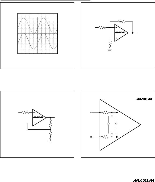
The MAX4091/MAX4092/MAX4094’s output voltage swings to within 15mV of the supplies with a 100kΩ load. This rail-to-rail swing at the input and the output substantially increases the dynamic range, especially in low-supply-voltage applications. Figure 1 shows the input and output waveforms for the MAX4092, configured as a unity-gain noninverting buffer operating from a single 3V supply. The input signal is 3.0VP-P, a 1kHz sinusoid centered at 1.5V. The output amplitude is approximately 2.98VP-P.
Input Offset Voltage
Rail-to-rail common-mode swing at the input is obtained by two complementary input stages in parallel, which feed a folded cascaded stage. The PNP stage is active for input voltages close to the negative rail, and the NPN stage is active for input voltages close to the positive rail.
The offsets of the two pairs are trimmed. However, there is some residual mismatch between them. This mismatch results in a two-level input offset characteristic, with a transition region between the levels occurring at a common-mode voltage of approximately 1.3V above VEE. Unlike other rail-to-rail op amps, the transition region has been widened to approximately 600mV in order to minimize the slight degradation in CMRR caused by this mismatch.
The input bias currents of the MAX4091/MAX4092/ MAX4094 are typically less than 20nA. The bias current flows into the device when the NPN input stage is active, and it flows out when the PNP input stage is active. To reduce the offset error caused by input bias current flowing through external source resistances,
match the effective resistance seen at each input. Connect resistor R3 between the noninverting input and ground when using the op amp in an inverting configuration (Figure 2a); connect resistor R3 between the noninverting input and the input signal when using the op amp in a noninverting configuration (Figure 2b). Select R3 to equal the parallel combination of R1 and R2. High source resistances will degrade noise performance, due to the the input current noise (which is multiplied by the source resistance).
Input Stage Protection Circuitry
The MAX4091/MAX4092/MAX4094 include internal protection circuitry that prevents damage to the precision input stage from large differential input voltages. This protection circuitry consists of back-to-back diodes between IN+ and INwith two 1.7kΩ resistors in series (Figure 3). The diodes limit the differential voltage applied to the amplifiers’ internal circuitry to no more than VF, where VF is the diodes’ forward-voltage drop (about 0.7V at +25°C).
Input bias current for the ICs (±20nA) is specified for small differential input voltages. For large differential input voltages (exceeding VF), this protection circuitry increases the input current at IN+ and IN-:
INPUT CURRENT = |
[(VIN+ ) − (VIN− )] − VF |
|
2 1.7kΩ |
||
|
Output Loading and Stability
Even with their low quiescent current of less than 130µA per op amp, the MAX4091/MAX4092/MAX4094 are well suited for driving loads up to 1kΩ while maintaining DC accuracy. Stability while driving heavy capacitive loads is another key advantage over comparable CMOS rail-to-rail op amps.
In op amp circuits, driving large capacitive loads increases the likelihood of oscillation. This is especially true for circuits with high-loop gains, such as a unitygain voltage follower. The output impedance and a capacitive load form an RC network that adds a pole to the loop response and induces phase lag. If the pole frequency is low enough—as when driving a large capacitive load––the circuit phase margin is degraded, leading to either an under-damped pulse response or oscillation.
The MAX4091/MAX4092/MAX4094 can drive capacitive loads in excess of 2000pF under certain conditions (Figure 4). When driving capacitive loads, the greatest potential for instability occurs when the op amp is sourcing approximately 200µA. Even in this case, stability is maintained with up to 400pF of output capaci-
8 _______________________________________________________________________________________

Single/Dual/Quad, Micropower, Single-Supply,
Rail-to-Rail Op Amps
tance. If the output sources either more or less current, stability is increased. These devices perform well with a 1000pF pure capacitive load (Figure 5). Figures 6a, 6b, and 6c show the performance with a 500pF load in parallel with various load resistors.
To increase stability while driving large-capacitive loads, connect a pullup resistor to VCC at the output to decrease the current the amplifier must source. If the amplifier is made to sink current rather than source, stability is further increased.
Frequency stability can be improved by adding an output isolation resistor (RS) to the voltage-follower circuit (Figure 7). This resistor improves the phase margin of the circuit by isolating the load capacitor from the op amp’s output. Figure 8a shows the MAX4092 driving 5000pF (RL ≥ 100kΩ), while Figure 8b adds a 47Ω isolation resistor.
Because the MAX4091/MAX4092/MAX4094 have excellent stability, no isolation resistor is required, except in the most demanding applications. This is beneficial because an isolation resistor would degrade the lowfrequency performance of the circuit.
Power-Up Settling Time
The MAX4091/MAX4092/MAX4094 have a typical supply current of 130µA per op amp. Although supply current is already low, it is sometimes desirable to reduce it further by powering down the op amp and associated ICs for periods of time. For example, when using a MAX4092 to buffer the inputs of a multi-channel analog- to-digital converter (ADC), much of the circuitry could be powered down between data samples to increase battery life. If samples are taken infrequently, the op amps, along with the ADC, may be powered down most of the time.
When power is reapplied to the MAX4091/MAX4092/
MAX4094, it takes some time for the voltages on the supply pin and the output pin of the op amp to settle. Supply settling time depends on the supply voltage, the value of the bypass capacitor, the output impedance of the incoming supply, and any lead resistance or inductance between components. Op amp settling time depends primarily on the output voltage and is slewrate limited. With the noninverting input to a voltage follower held at midsupply (Figure 9), when the supply steps from 0 to VCC, the output settles in approximately 2µs for VCC = 3V (Figure 10a) and 8µs for VCC = 5V (Figure 10b).
Power Supplies and Layout
The MAX4091/MAX4092/MAX4094 operate from a single 2.7V to 6V power supply, or from dual supplies of ±1.35V to ±3V. For single-supply operation, bypass the power supply with a 0.1µF capacitor. If operating from dual supplies, bypass each supply to ground.
Good layout improves performance by decreasing the amount of stray capacitance at the op amp’s inputs and output. To decrease stray capacitance, minimize both trace lengths and resistor leads and place external components close to the op amp’s pins.
Chip Information
MAX4091 TRANSISTOR COUNT: 168
MAX4092 TRANSISTOR COUNT: 336
MAX4094 TRANSISTOR COUNT: 670
PROCESS: Bipolar
MAX4091/MAX4092/MAX4094
_______________________________________________________________________________________ 9
MAX4091/MAX4092/MAX4094
Single/Dual/Quad, Micropower, Single-Supply,
Rail-to-Rail Op Amps
Test Circuits/Timing Diagrams
VCC = 3V
VEE = 0
VIN
1V/div
VOUT
1V/div
200µs/div
Figure 1. Rail-to-Rail Input and Output Operation
R3
VIN
VOUT
MAX409_
R2
R3 = R2 II R1
R1
Figure 2b. Reducing Offset Error Due to Bias Current: Noninverting Configuration
R2
R1
VIN
VOUT
MAX409_
R3 |
R3 = R2 II R1 |
Figure 2a. Reducing Offset Error Due to Bias Current: Inverting Configuration
|
|
MAX4091 |
|
|
MAX4092 |
1.7kΩ |
TO INTERNAL |
MAX4094 |
IN+ |
CIRCUITRY |
|
|
|
|
IN– |
TO INTERNAL |
|
|
|
|
1.7kΩ |
CIRCUITRY |
|
Figure 3. Input Stage Protection Circuitry
10 ______________________________________________________________________________________