

бакМИТ_КП2015 / Компоненты по вариантам / Операционные_усилители / LTC6084HMS8
.pdfFEATURES
n |
Low Offset Voltage: 750μV Maximum |
n |
Low Offset Drift: 5μV/°C Maximum |
n |
Low Input Bias Current: |
|
1pA (Typical at 25°C) |
|
40pA (≤85°C) |
n |
Rail-to-Rail Inputs and Outputs |
n |
2.5V to 5.5V Operation Voltage |
n |
Gain Bandwidth Product: 1.5MHz |
n |
CMRR: 70dB Minimum |
n |
PSRR: 94dB Minimum |
n |
Supply Current: 110μA per Amplifier |
n |
Shutdown Current: 1.1μA per Amplifier |
n |
Available in 8-Lead MSOP and 10-Lead DFN |
|
Packages (LTC6084) and 16-Lead SSOP and DFN |
|
Packages (LTC6085) |
APPLICATIONS
n Portable Test Equipment
n Medical Equipment
n Consumer Electronics
n Data Acquisition
Dual/Quad 1.5MHz, Rail-to-Rail, CMOS Amplifiers
DESCRIPTION
TheLTC®6084/LTC6085aredual/quad,lowcost,lowoffset, rail-to-railinput/output,unity-gainstableCMOSoperational amplifiers that feature 1pA of input bias current.
A 1.5MHz gain bandwidth, and 0.5V/μs slew rate, along with the wide supply range and a low 0.75mV offset, make the LTC6084/LTC6085 useful in an extensive variety of applications from data acquisition to medical equipment and consumer electronics. The 110μA supply current and the shutdownmodeareidealforsignalprocessingapplications which demand performance with minimal power.
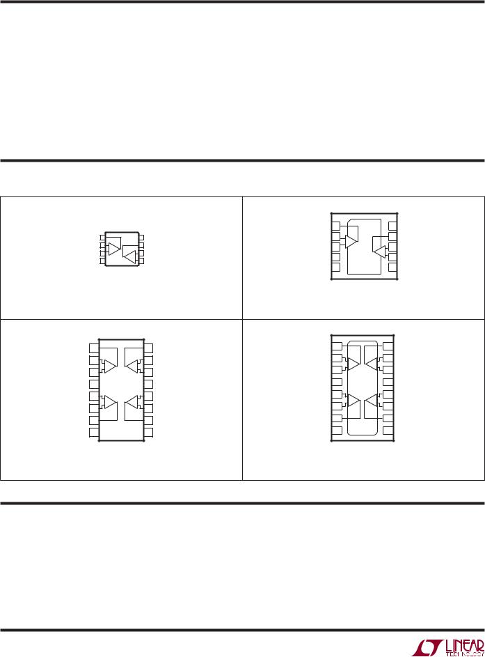
The LTC6084/LTC6085 have an output stage which swings within 5mV of either supply rail to maximize signal dynamic range in low supply applications. The input common mode range includes the entire supply voltage. These op amps are specified on power supply voltages of 2.5V and 5V from –40°C to 125°C. The dual amplifier LTC6084 is available in 8-lead MSOP and 10-lead DFN packages. The quad amplifier LTC6085 is available in 16-lead SSOP and DFN packages.
L, LT, LTC and LTM are registered trademarks of Linear Technology Corporation. All other trademarks are the property of their respective owners.
TYPICAL APPLICATION
Shock Sensor Amplifier
|
|
|
200k |
|
|
20M |
470pF |
|
|
|
|
3V |
|
|
|
20M |
– |
|
|
|
|
1/2 |
|
|
2k |
* |
|
|
|
LTC6084 |
|
|||
100k |
|
VOUT = 120mV/g |
||
|
+ |
|
||
3V |
|
|
|
|
100k |
|
|
|
|
|
0.22μF |
|
|
|
|
|
|
|
60845 TA01 |
|
|
7Hz TO 5kHz |
|
|
*SHOCK SENSOR MURATA ERIE PKGS-OOMX1 www.murata.com
Input Bias Current
vs Common Mode Voltage
|
10000 |
VS = 5V |
|
|
|
|
|
|
|
|
|
|
|
|
|
|
|
|
|
|
|
||
(pA) |
1000 |
|
|
|
|
TA |
= 125°C |
|
|
|
|
|
|
|
|
|
|
|
|
||||
100 |
|
|
|
|
|
|
|
|
|
|
|
CURRENT |
|
|
|
|
|
|
|
|
|
|
|
|
|
|
|
|
TA = 85°C |
|
|
|
|||
10 |
|
|
|
|
|
|
|
|
|
|
|
BIAS |
|
|
|
|
|
TA = 25°C |
|
|
|
||
1 |
|
|
|
|
|
|
|
|
|
|
|
INPUT |
|
|
|
|
|
|
|
|
|
|
|
0.1 |
|
|
|
|
|
|
|
|
|
|
|
|
|
|
|
|
|
|
|
|
|
|
|
|
0.01 |
0.5 |
1 |
1.5 |
2 |
2.5 |
3 |
3.5 |
4 |
4.5 |
5 |
|
0 |
||||||||||
|
|
|
COMMON MODE VOLTAGE (V) |
|
|
||||||
|
|
|
|
|
|
|
|
|
|
60845 TA01b |
|
60845fa
1
LTC6084/LTC6085
ABSOLUTE MAXIMUM RATINGS (Note 1)
Total Supply Voltage (V+ to V–) ................................... |
6V |
Input Voltage...................................................... |
V– to V+ |
Input Current........................................................ |
±10mA |
SHDNA/SHDNB Voltage..................................... |
V– to V+ |
Output Short-Circuit Duration (Note 2) ............ |
Indefinite |
Operating Temperature Range (Note 3) |
|
LTC6084C/LTC6085C ........................... |
–40°C to 85°C |
LTC6084H/LTC6085H......................... |
–40°C to 125°C |
Specified Temperature Range (Note 4) |
|
LTC6084C/LTC6085C ............................... |
0°C to 70°C |
LTC6084H/LTC6085H........................... |
–40°C to 125° |
Junction Temperature ........................................... |
150°C |
Storage Temperature Range................... |
–65°C to 125°C |
Lead Temperature (Soldering, 10 sec) |
|
MS8, GN Only................................................... |
300°C |
PIN CONFIGURATION |
|
|
|
|
|
|
|
|
||||
|
|
|
|
|
|
|
|
TOP VIEW |
|
|
|
|
|
|
TOP VIEW |
|
|
OUTA |
1 |
|
|
|
10 |
V+ |
|
OUTA |
1 |
|
|
8 V+ |
–INA |
2 |
– |
|
|
9 |
OUTB |
|
–INA |
2 |
–A |
|
7 OUTB |
+INA |
3 |
+A |
11 |
– |
8 |
–INB |
|
+INA |
3 |
+ |
– |
6 –INB |
V– |
4 |
|
|
B |
7 |
+INB |
|
V– |
4 |
|
B |
5 +INB |
|
|
+ |
|||||
|
+ |
SHDNA |
5 |
|
|
|
6 |
SHDNB |
||||
|
|
MS8 PACKAGE |
|
|
|
|
|
|||||
|
|
|
|
|
|
|
|
|
|
|
||
|
8-LEAD PLASTIC MSOP |
|
|
|
DD PACKAGE |
|
|
|||||
TJMAX = 150°C, θJA = 200°C/W |
|
|
|
|
||||||||
10-LEAD (3mm × 3mm) PLASTIC DFN |
||||||||||||
|
|
|
|
|
|
TJMAX = 150°C, θJA = 43°C/W |
||||||
|
|
|
|
|
|
EXPOSED PAD (PIN 11) IS V–, MUST BE SOLDERED TO PCB |
||||||
|
|
TOP VIEW |
|
|
|
|
TOP VIEW |
|
|
|
||
|
|
|
|
|
|
|
|
|
|
|
||
OUTA |
1 |
|
|
16 |
OUTD |
OUTA |
1 |
|
|
|
16 |
OUTD |
|
|
|
|
|
|
|
|
|
||||
–INA |
2 |
– |
– |
15 |
–IND |
–INA |
2 |
– |
– |
|
15 |
–IND |
|
|
|
|
|
|
A |
D |
|
|
|
||
|
|
A |
D |
|
|
+INA |
3 |
+ |
+ |
|
14 |
+IND |
+INA |
3 |
+ |
+ |
14 |
+IND |
|
|
|
||||
|
|
V+ |
|
|
|
|
13 V– |
|||||
V+ |
4 |
|
|
13 V– |
4 |
|
17 |
|
||||
|
|
|
|
|
|
+INB |
5 |
|
|
12 |
+INC |
|
+INB |
5 |
+ |
+ |
12 |
+INC |
+B |
+ |
|
||||
|
|
C |
|
|
|
|||||||
|
|
B |
C |
|
|
–INB |
6 |
– |
– |
|
11 |
–INC |
–INB |
6 |
– |
– |
11 |
–INC |
|
|
|
||||
|
|
|
|
|
|
|
|
|
||||
OUTB |
7 |
|
|
10 |
OUTC |
OUTB |
7 |
|
|
|
10 |
OUTC |
|
|
|
|
|
|
|
|
|
||||
NC |
8 |
|
|
9 |
NC |
NC |
8 |
|
|
|
9 |
NC |
|
|
|
|
|
|
|
|
|
||||
GN PACKAGE |
DHC PACKAGE |
|
16-LEAD PLASTIC SSOP NARROW |
16-LEAD (5mm × 3mm) PLASTIC DFN |
|
TJMAX = 150°C, θJA = 110°C/W |
TJMAX = 150°C, θJA = 43°C/W |
|
EXPOSED PAD (PIN 17) IS V–, MUST BE SOLDERED TO PCB |
||
|
ORDER INFORMATION
LEAD FREE FINISH |
TAPE AND REEL |
PART MARKING* |
PACKAGE DESCRIPTION |
SPECIFIED TEMPERATURE RANGE |
|
|
|
|
|
LTC6084CMS8#PBF |
LTC6084CMS8#TRPBF |
LTDNG |
8-Lead Plastic MSOP |
0°C to 70°C |
|
|
|
|
|
LTC6084HMS8#PBF |
LTC6084HMS8#TRPBF |
LTDNG |
8-Lead Plastic MSOP |
–40°C to 125°C |
|
|
|
|
|
LTC6084CDD#PBF |
LTC6084CDD#TRPBF |
LDNH |
10-Lead (3mm × 3mm) Plastic DFN |
0°C to 70°C |
|
|
|
|
|
LTC6084HDD#PBF |
LTC6084HDD#TRPBF |
LDNH |
10-Lead (3mm × 3mm) Plastic DFN |
–40°C to 125°C |
|
|
|
|
|
60845fa
2

LTC6084/LTC6085
ORDER INFORMATION
LEAD FREE FINISH |
TAPE AND REEL |
PART MARKING* |
PACKAGE DESCRIPTION |
SPECIFIED TEMPERATURE RANGE |
|
|
|
|
|
LTC6085CGN#PBF |
LTC6085CGN#TRPBF |
6085 |
16-Lead Plastic SSOP |
0°C to 70°C |
|
|
|
|
|
LTC6085HGN#PBF |
LTC6085HGN#TRPBF |
6085 |
16-Lead Plastic SSOP |
–40°C to 125°C |
|
|
|
|
|
LTC6085CDHC#PBF |
LTC6085CDHC#TRPBF |
6085 |
16-Lead (5mm × 3mm) Plastic DFN |
0°C to 70°C |
|
|
|
|
|
LTC6085HDHC#PBF |
LTC6085HDHC#TRPBF |
6085 |
16-Lead (5mm × 3mm) Plastic DFN |
–40°C to 125°C |
Consult LTC Marketing for parts specified with wider operating temperature ranges. *The temperature grade is identified by a label on the shipping container. Consult LTC Marketing for information on non-standard lead based finish parts.
For more information on lead free part marking, go to: http://www.linear.com/leadfree/
For more information on tape and reel specifications, go to: http://www.linear.com/tapeandreel/
ELECTRICAL CHARACTERISTICS The l denotes the specifications which apply over the full operating temperature range, otherwise specifications are at TA = 25°C. Test conditions are V+ = 2.5V, V– = 0V, VCM = 0.5V unless otherwise noted.
|
|
|
|
|
|
C SUFFIX |
|
|
H SUFFIX |
|
|
SYMBOL |
PARAMETER |
CONDITIONS |
|
MIN |
TYP |
MAX |
MIN |
TYP |
MAX |
UNITS |
|
|
|
|
|
|
|
|
|
|
|
|
|
VOS |
Offset Voltage (Note 5) |
LTC6084MS8, LTC6085GN |
|
|
300 |
750 |
|
300 |
750 |
μV |
|
|
|
|
LTC6084DD, LTC6085DHC |
|
|
300 |
1100 |
|
300 |
1100 |
μV |
|
|
|
LTC6084MS8, LTC6085GN |
l |
|
|
900 |
|
|
1100 |
μV |
|
|
|
LTC6084DD, LTC6085DHC |
l |
|
|
1350 |
|
|
1600 |
μV |
|
|
|
|
|
|
|
|
|
|
|
|
VOS/ T |
Input Offset Voltage Drift |
|
l |
|
2 |
5 |
|
2 |
5 |
μV/°C |
|
|
(Note 6) |
|
|
|
|
|
|
|
|
|
|
|
|
|
|
|
|
|
|
|
|
|
|
IB |
Input Bias Current |
Guaranteed by 5V Test |
|
|
1 |
40 |
|
1 |
750 |
pA |
|
|
(Notes 5, 7) |
|
l |
|
|
|
|
pA |
|||
IOS |
Input Offset Current |
Guaranteed by 5V Test |
|
|
0.5 |
30 |
|
0.5 |
150 |
pA |
|
|
(Notes 5, 7) |
|
l |
|
|
|
|
pA |
|||
en |
Input Noise Voltage |
f = 1kHz |
|
|
31 |
|
|
31 |
|
nV/√Hz |
|
|
Density |
f = 10kHz |
|
|
27 |
|
|
27 |
|
nV/√Hz |
|
|
Input Noise Voltage |
0.1Hz to 10Hz |
|
|
3 |
|
|
3 |
|
μVP-P |
|
in |
Input Noise Current |
|
|
|
0.56 |
|
|
0.56 |
|
fA/√Hz |
|
|
Density (Note 8) |
|
|
|
|
|
|
|
|
|
|
|
Input Common Mode |
|
l |
V– |
|
V+ |
V– |
|
V+ |
V |
|
|
Range |
|
|
|
|
|
|
|
|
|
|
|
|
|
|
|
|
|
|
|
|
|
|
CIN |
Input Capacitance |
f = 100kHz |
|
|
5 |
|
|
5 |
|
pF |
|
|
|
Differential Mode |
|
|
|
|
|
|
|||
|
|
Common Mode |
|
|
|
9 |
|
|
9 |
|
pF |
|
|
|
|
|
|
|
|
|
|
|
|
CMRR |
Common Mode Rejection |
0 ≤ VCM ≤ 2.5V |
|
64 |
80 |
|
64 |
80 |
|
dB |
|
|
Ratio |
|
l |
63 |
|
|
61 |
|
|
dB |
|
PSRR |
Power Supply Rejection |
VS = 2.5V to 5.5V |
|
94 |
115 |
|
94 |
115 |
|
dB |
|
|
Ratio |
|
l |
91 |
|
|
89 |
|
|
dB |
|
VOUT |
Output Voltage, High, |
No Load |
l |
|
0.5 |
5 |
|
0.5 |
10 |
mV |
|
|
(Referred to V+) |
ISOURCE = 1mA |
l |
|
39 |
85 |
|
39 |
100 |
mV |
|
|
|
|
ISOURCE = 5mA |
l |
|
220 |
460 |
|
220 |
|
mV |
|
|
|
|
|
|
|
|
|
|
|
|
|
Output Voltage, Low, |
No Load |
l |
|
0.5 |
5 |
|
0.5 |
10 |
mV |
|
|
(Referred to V–) |
ISINK = 1mA |
l |
|
36 |
85 |
|
36 |
100 |
mV |
|
|
|
|
ISINK = 5mA |
l |
|
200 |
460 |
|
200 |
|
mV |
|
|
|
|
|
|
|
|
|
|
|
|
AVOL |
Large-Signal Voltage Gain |
RLOAD = 10k, 0.4V ≤ VOUT ≤ 2.1V |
|
400 |
2000 |
|
400 |
2000 |
|
V/mV |
|
|
|
|
|
l |
200 |
|
|
150 |
|
|
V/mV |
|
|
|
|
|
|
|
|
|
|
|
60845fa |
|
|
|
|
|
|
|
|
|
|
|
|
|
|
|
|
|
|
|
|
|
|
|
|
|
|
|
|
|
|
|
|
|
|
|
3 |
|
|
|
|
|
|
|
|
|
|
|
|
|
|
|
|
|
|
|
|
|
|
|
|

LTC6084/LTC6085
ELECTRICAL CHARACTERISTICS The l denotes the specifications which apply over the full operating temperature range, otherwise specifications are at TA = 25°C. Test conditions are V+ = 2.5V, V– = 0V, VCM = 0.5V unless otherwise noted.
|
|
|
|
|
C SUFFIX |
|
|
H SUFFIX |
|
|
SYMBOL |
PARAMETER |
CONDITIONS |
|
MIN |
TYP |
MAX |
MIN |
TYP |
MAX |
UNITS |
|
|
|
|
|
|
|
|
|
|
|
ISC |
Output Short-Circuit |
Source and Sink |
|
7.7 |
12.5 |
|
7.7 |
12.5 |
|
mA |
|
Current |
|
l |
6 |
|
|
4.5 |
|
|
mA |
SR |
Slew Rate |
AV = 1 |
|
|
0.5 |
|
|
0.5 |
|
V/μs |
GBW |
Gain Bandwidth Product |
RLOAD = 50k, VCM = 1.25V |
|
0.9 |
1.5 |
|
0.9 |
1.5 |
|
MHz |
|
(fTEST = 10kHz) |
|
l |
0.7 |
|
|
0.6 |
|
|
|
|
|
|
|
|
|
|
|
|||
Φ0 |
Phase Margin |
RL = 10k, CL = 150pF, AV = 1 |
|
|
45 |
|
|
45 |
|
Deg |
tS |
Settling Time 0.1% |
VSTEP = 1V, AV = 1 |
|
|
6 |
|
|
6 |
|
μs |
IS |
Supply Current |
No Load |
|
|
110 |
130 |
|
110 |
130 |
μA |
|
(Per Amplifier) |
|
l |
|
|
140 |
|
|
145 |
μA |
|
Shutdown Current |
Shutdown, VSHDNx ≤ 0.5V |
l |
|
0.2 |
0.3 |
|
0.2 |
0.5 |
μA |
|
(Per Amplifier) |
|
|
|
|
|
|
|
|
|
VS |
Supply Voltage Range |
Guaranteed by the PSRR Test |
l |
2.5 |
|
5.5 |
2.5 |
|
5.5 |
V |
|
|
|
||||||||
|
Channel Separation |
fS = 10kHz |
|
|
–120 |
|
|
–120 |
|
dB |
|
Shutdown Logic |
SHDNx High |
|
1.8 |
|
|
1.8 |
|
|
V |
|
|
SHDNx Low |
|
|
|
0.5 |
|
|
0.5 |
V |
tON |
Turn On Time |
VSHDNx = 0.5V to 1.8V |
|
|
7 |
|
|
7 |
|
μs |
tOFF |
Turn Off Time |
VSHDNx = 1.8V to 0.5V |
|
|
1 |
|
|
1 |
|
μs |
|
Leakage of SHDN Pin |
VSHDNx = 0V |
l |
|
0.2 |
0.3 |
|
0.2 |
0.5 |
μA |
|
|
|
|
The l denotes the specifications which apply over the full operating temperature range, otherwise specifications are at TA = 25°C. Test conditions are V+ = 5V, V– = 0V, VCM = 0.5V unless otherwise noted.
|
|
|
|
|
C SUFFIX |
|
|
H SUFFIX |
|
|
SYMBOL |
PARAMETER |
CONDITIONS |
|
MIN |
TYP |
MAX |
MIN |
TYP |
MAX |
UNITS |
|
|
|
|
|
|
|
|
|
|
|
VOS |
Offset Voltage (Note 5) |
LTC6084MS8, LTC6085GN |
|
|
300 |
750 |
|
300 |
750 |
μV |
|
|
LTC6084DD, LTC6085DHC |
|
|
300 |
1100 |
|
300 |
1100 |
μV |
|
|
LTC6084MS8, LTC6085GN |
l |
|
|
900 |
|
|
1100 |
μV |
|
|
LTC6084DD, LTC6085DHC |
l |
|
|
1350 |
|
|
1600 |
μV |
VOS/ T |
Input Offset Voltage Drift |
|
l |
|
2 |
5 |
|
2 |
5 |
μV/°C |
|
(Note 6) |
|
|
|
|
|
|
|
|
|
|
|
|
|
|
|
|
|
|
|
|
IB |
Input Bias Current |
|
|
|
1 |
40 |
|
1 |
750 |
pA |
|
(Notes 5, 7) |
|
l |
|
|
|
|
pA |
||
IOS |
Input Offset Current |
|
|
|
0.5 |
30 |
|
0.5 |
150 |
pA |
|
(Notes 5, 7) |
|
l |
|
|
|
|
pA |
||
en |
Input Noise Voltage |
f = 1kHz |
|
|
31 |
|
|
31 |
|
nV/√Hz |
|
Density |
f = 10kHz |
|
|
27 |
|
|
27 |
|
nV/√Hz |
|
Input Noise Voltage |
0.1Hz to 10Hz |
|
|
3 |
|
|
3 |
|
μVP-P |
in |
Input Noise Current |
|
|
|
0.56 |
|
|
0.56 |
|
fA/√Hz |
|
Density (Note 8) |
|
|
|
|
|
|
|
|
|
|
Input Common Mode |
|
l |
V– |
|
V+ |
V– |
|
V+ |
V |
|
Range |
|
|
|
|
|
|
|
|
|
CIN |
Input Capacitance |
f = 100kHz |
|
|
5 |
|
|
5 |
|
pF |
|
Differential Mode |
|
|
|
|
|
|
|||
|
Common Mode |
|
|
|
9 |
|
|
9 |
|
pF |
|
|
|
|
|
|
|
|
|
|
60845fa |
4

LTC6084/LTC6085
ELECTRICAL CHARACTERISTICS The l denotes the specifications which apply over the full operating temperature range, otherwise specifications are at TA = 25°C. Test conditions are V+ = 5V, V– = 0V, VCM = 0.5V unless otherwise noted.
|
|
|
|
|
|
C SUFFIX |
|
|
H SUFFIX |
|
|
SYMBOL |
PARAMETER |
|
CONDITIONS |
|
MIN |
TYP |
MAX |
MIN |
TYP |
MAX |
UNITS |
|
|
|
|
|
|
|
|
|
|
|
|
CMRR |
Common Mode Rejection |
0 ≤ VCM ≤ 5V |
|
70 |
84 |
|
70 |
84 |
|
dB |
|
|
Ratio |
|
|
l |
68 |
|
|
66 |
|
|
dB |
PSRR |
Power Supply Rejection |
VS = 2.5V to 5.5V |
|
94 |
115 |
|
94 |
115 |
|
dB |
|
|
Ratio |
|
|
l |
91 |
|
|
89 |
|
|
dB |
VOUT |
Output Voltage, High, |
No Load |
l |
|
0.5 |
5 |
|
0.5 |
10 |
mV |
|
|
|
|
|||||||||
|
+ |
) |
ISOURCE = 1mA |
l |
|
39 |
85 |
|
39 |
100 |
mV |
|
(Referred to V |
|
|
|
|||||||
|
|
|
ISOURCE = 5mA |
l |
|
220 |
460 |
|
220 |
|
mV |
|
|
|
|
|
|
|
|||||
|
Output Voltage, Low, |
No Load |
l |
|
0.5 |
5 |
|
0.5 |
10 |
mV |
|
|
– |
) |
ISINK = 1mA |
l |
|
36 |
85 |
|
36 |
100 |
mV |
|
(Referred to V |
|
|
|
|||||||
|
|
|
ISINK = 5mA |
l |
|
200 |
460 |
|
200 |
|
mV |
|
|
|
|
|
|
|
|||||
AVOL |
Large-Signal Voltage Gain |
RLOAD = 10k, 0.5V ≤ VOUT ≤ 4.5V |
|
1000 |
5000 |
|
1000 |
5000 |
|
V/mV |
|
|
|
|
|
l |
400 |
|
|
300 |
|
|
V/mV |
ISC |
Output Short-Circuit |
Source and Sink |
|
7.7 |
12.5 |
|
7.7 |
12.5 |
|
mA |
|
|
Current |
|
|
l |
6 |
|
|
4.5 |
|
|
mA |
SR |
Slew Rate |
|
AV = 1 |
|
|
0.5 |
|
|
0.5 |
|
V/μs |
GBW |
Gain Bandwidth Product |
RLOAD = 50k, VCM = 2.5V |
|
0.9 |
1.5 |
|
0.9 |
1.5 |
|
MHz |
|
|
(fTEST = 10kHz) |
|
l |
0.7 |
|
|
0.6 |
|
|
|
|
|
|
|
|
|
|
|
|
||||
Φ0 |
Phase Margin |
|
RL = 10k, CL = 150pF, AV = 1 |
|
|
45 |
|
|
45 |
|
Deg |
tS |
Settling Time 0.1% |
VSTEP = 1V, AV = 1 |
|
|
5 |
|
|
5 |
|
μs |
|
IS |
Supply Current |
|
No Load |
|
|
110 |
130 |
|
110 |
130 |
μA |
|
(Per Amplifier) |
|
|
l |
|
|
140 |
|
|
145 |
μA |
|
Shutdown Current |
Shutdown, VSHDNx ≤ 1.2V |
l |
|
1.1 |
1.8 |
|
1.1 |
2 |
μA |
|
|
(Per Amplifier) |
|
|
|
|
|
|
|
|
|
|
VS |
Supply Voltage Range |
Guaranteed by the PSRR Test |
l |
2.5 |
|
5.5 |
2.5 |
|
5.5 |
V |
|
|
|
|
|||||||||
|
Channel Separation |
fS = 10kHz |
|
|
–120 |
|
|
–120 |
|
dB |
|
|
Shutdown Logic |
SHDNx High |
|
3.5 |
|
|
3.5 |
|
|
V |
|
|
|
|
SHDNx Low |
|
|
|
1.2 |
|
|
1.2 |
V |
|
|
|
|
|
|
|
|
|
|
|
|
tON |
Turn On Time |
|
VSHDNx = 1.2V to 3.5V |
|
|
7 |
|
|
7 |
|
μs |
tOFF |
Turn Off Time |
|
VSHDNx = 3.5V to 1.2V |
|
|
1 |
|
|
1 |
|
μs |
|
Leakage of SHDN Pin |
VSHDNx = 0V |
l |
|
0.5 |
0.9 |
|
0.5 |
1.2 |
μA |
|
|
|
|
|
||||||||
Note 1: Stresses beyond those listed under Absolute Maximum Ratings may cause permanent damage to the device. Exposure to any Absolute Maximum Rating condition for extended periods may affect device reliability and lifetime.
Note 2: A heat sink may be required to keep the junction temperature below the absolute maximum. This depends on the power supply voltage and the total output current.
Note 3: The LTC6084C/LTC6085C are guaranteed functional over the operating temperature range of –40°C to 85°C. The LTC6084H/LTC6085H are guaranteed functional over the operating temperature range of –40°C to 125°C.
Note 4: The LTC6084C/LTC6085C are guaranteed to meet specified performance from 0°C to 70°C. The LTC6084C/LTC6085C are designed, characterized and expected to meet specified performance from –40°C to 85°C but are not tested or QA sampled at these temperatures. The LTC6084H/LTC6085H are guaranteed to meet specified performance from –40°C to 125°C.
Note 5: ESD (Electrostatic Discharge) sensitive device. ESD protection devices are used extensively internal to the LTC6084/LTC6085; however, high electrostatic discharge can damage or degrade the device. Use proper ESD handling precautions.
Note 6: This parameter is not 100% tested.
Note 7: This specification is limited by high speed automated test capability. See Typical Performance Characteristic curves for actual performance.
Note 8: Current noise is calculated from in = √2qIB, where q = 1.6 • 10–19 coulombs.
60845fa
5
LTC6084/LTC6085
TYPICAL PERFORMANCE CHARACTERISTICS
|
20 |
VOS Distribution |
|
|
|
|
|
|
1.0 |
VOS vs VCM |
|
|
|
|
|
|
|
|
||||
|
LTC6084 MS8 |
|
|
|
|
|
|
VS = 5V |
|
|
|
|
|
|
|
|
|
30 |
||||
|
18 |
|
|
|
|
|
|
0.8 |
|
|
|
|
|
|
|
|
|
28 |
||||
|
VS = 5V |
|
|
|
|
|
|
TA = 25°C |
|
|
|
|
|
|
|
|
26 |
|||||
|
16 |
VCM = 0.5V |
|
|
|
|
|
|
0.6 |
REPRESENTATIVE PARTS |
|
|
|
|
|
|||||||
PERCENTAGE OF UNITS (%) |
|
|
|
|
|
|
|
|
|
|
|
24 |
||||||||||
TA = 25°C |
|
|
|
|
|
|
|
|
|
|
|
|
|
|
|
|
PERCENT OF UNITS (%) |
|||||
14 |
100 UNITS |
|
|
|
|
|
|
0.4 |
|
|
|
|
|
|
|
|
|
|
22 |
|||
12 |
|
|
|
|
|
|
|
|
0.2 |
|
|
|
|
|
|
|
|
|
|
20 |
||
|
|
|
|
|
|
|
(mV) |
|
|
|
|
|
|
|
|
|
|
18 |
||||
10 |
|
|
|
|
|
|
|
0.0 |
|
|
|
|
|
|
|
|
|
|
16 |
|||
|
|
|
|
|
|
|
OS |
|
|
|
|
|
|
|
|
|
|
14 |
||||
8 |
|
|
|
|
|
|
|
–0.2 |
|
|
|
|
|
|
|
|
|
|
||||
|
|
|
|
|
|
|
V |
|
|
|
|
|
|
|
|
|
|
12 |
||||
6 |
|
|
|
|
|
|
|
–0.4 |
|
|
|
|
|
|
|
|
|
|
10 |
|||
|
|
|
|
|
|
|
|
|
|
|
|
|
|
|
|
|
8 |
|||||
4 |
|
|
|
|
|
|
|
–0.6 |
|
|
|
|
|
|
|
|
|
|
||||
|
|
|
|
|
|
|
|
|
|
|
|
|
|
|
|
|
6 |
|||||
|
|
|
|
|
|
|
|
|
|
|
|
|
|
|
|
|
|
|
|
|||
|
2 |
|
|
|
|
|
|
|
|
–0.8 |
|
|
|
|
|
|
|
|
|
|
|
4 |
|
|
|
|
|
|
|
|
|
|
|
|
|
|
|
|
|
|
|
|
2 |
||
|
0 |
|
|
|
|
|
|
|
|
–1.0 |
|
|
|
|
|
|
|
|
|
|
|
|
|
–1 |
–0.8 –0.6 –0.4 –0.2 |
0 |
0.2 |
0.4 |
0.6 |
0.8 |
1 |
0 |
0.5 |
1 |
1.5 |
2 |
2.5 |
3 |
3.5 |
4 |
4.5 |
5 |
0 |
||
|
|
|
|
|||||||||||||||||||
|
|
|
VOS (mV) |
|
|
60845 G01 |
|
|
|
|
|
|
VCM (V) |
|
|
|
60845 G02 |
|
||||
VOS Drift Distribution
|
|
|
|
|
|
|
LTC6084 MS8 |
|||
|
|
|
|
|
|
|
|
VS = 5V |
||
|
|
|
|
|
|
|
|
VCM = 2.5V |
||
|
|
|
|
|
TA = –40°C TO 125°C |
|||||
|
|
|
|
|
|
|
|
78 UNITS |
||
–1 –0.5 |
0 |
0.5 |
1 |
1.5 |
2 |
2.5 |
3 |
3.5 |
4 |
4.5 |
DISTRIBUTION (μV/°C)
60845 G03
|
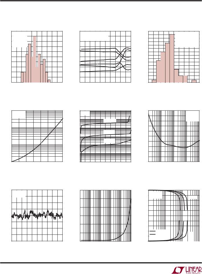
Input Bias Current |
|
Input Bias vs Temperature |
vs Common Mode Voltage |
Input Noise Voltage vs Frequency |
INPUT BIAS CURRENT (pA)
1000 |
|
|
|
|
|
|
|
10000 |
VS = 5V |
|
|
|
|
|
|
|
|
100 |
|
|
|
VS = 5V |
|
VS = 5V |
|
|
|
|
|
|
|
|
|
|
|
|
|
|
|
90 |
|
|
|
||||
VCM = 2.5V |
|
|
|
|
|
|
|
|
|
|
|
|
|
|
|
|
|
|
|
VCM = 2.5V |
|||
|
|
|
|
|
|
|
|
1000 |
|
|
|
|
TA |
= 125°C |
|
|
|
80 |
|
|
TA = 25°C |
||
|
|
|
|
|
|
|
|
BIASINPUTCURRENT (pA) |
|
|
|
|
|
|
|
|
|
|
|
||||
|
|
|
|
|
|
|
|
|
|
|
|
|
|
|
|
|
|
NOISEINPUTVOLTAGE (nV/√Hz) |
|
|
|
|
|
100 |
|
|
|
|
|
|
|
100 |
|
|
|
|
|
|
|
|
|
|
70 |
|
|
|
|
|
|
|
|
|
|
|
|
|
|
|
|
|
TA = 85°C |
|
|
|
60 |
|
|
|
|
||
|
|
|
|
|
|
|
|
10 |
|
|
|
|
|
|
|
|
|
|
50 |
|
|
|
|
|
|
|
|
|
|
|
|
|
|
|
|
|
TA = 25°C |
|
|
|
40 |
|
|
|
|
||
10 |
|
|
|
|
|
|
|
1 |
|
|
|
|
|
|
|
|
|
|
30 |
|
|
|
|
|
|
|
|
|
|
|
|
|
|
|
|
|
|
|
|
|
|
|
|
|
|
|
|
|
|
|
|
|
|
|
|
0.1 |
|
|
|
|
|
|
|
|
|
|
20 |
|
|
|
|
|
|
|
|
|
|
|
|
|
|
|
|
|
|
|
|
|
|
10 |
|
|
|
|
|
|
|
|
|
|
|
|
|
|
|
|
|
|
|
|
|
|
|
|
|
|
|
|
|
1 |
40 |
55 |
70 |
85 |
100 |
115 |
130 |
0.01 |
0.5 |
1 |
1.5 |
2 |
2.5 |
3 |
3.5 |
4 |
4.5 |
5 |
0 |
100 |
1k |
10k |
100k |
25 |
0 |
10 |
|||||||||||||||||||||
|
|
TEMPERATURE (°C) |
60845 G04 |
|
|
COMMON MODE VOLTAGE (V) |
|
|
|
|
FREQUENCY (Hz) |
|
60845 G06 |
||||||||||
|
|
|
|
|
|
|
|
|
|
|
|
|
|
|
60845 G05 |
|
|
|
|
||||
0.1Hz to 10Hz Output Voltage |
|
Output Saturation Voltage |
Noise |
Input Noise Current vs Frequency |
vs Load Current (Output High) |
|
VS = 5V |
600 |
|
|
|
(V) |
|
(2μV/DIV)VOLTAGENOISEINPUT |
VCM = 2.5V |
|
|
)(fA/√CURRENTNOISEHz |
500 |
VOLTAGESATURATIONHIGHOUTPUT |
|
|
|
|
|
|
|
400 |
|
|
|
300 |
|
|
|
200 |
|
|
|
100 |
|
|
|
0 |
|
1 |
10 |
100 |
1k |
10k |
100k |
TIME (1s/DIV) |
|
FREQUENCY (Hz) |
|
|
|
60845 G07 |
|
|
|
||
|
|
|
|
60845 G08 |
|
5.0 |
VS = 5V |
|
||
4.5 |
|
|||
V |
CM |
= 2.5V |
SOURCE |
|
4.0 |
|
|
||
|
|
|
|
|
3.5
3.0
2.5
2.0
1.5
1.0 |
|
|
|
|
TA = –55°C |
|
|
|
|
|
|
|||||||
|
|
|
|
|
|
|||||||||||||
0.5 |
|
|
|
|
TA = 25°C |
|
SINK |
|
||||||||||
|
|
|
|
|
|
|
|
|
|
|||||||||
|
|
|
|
TA = 125°C |
|
|
|
|
|
|
||||||||
0.0 |
|
|
|
|
|
|
|
|
|
|
||||||||
|
|
|
|
|
|
|
|
|
|
|
|
|
|
|
|
|
|
|
|
|
|
1 |
10 |
100 |
|||||||||||||
0.1 |
||||||||||||||||||
LOAD CURRENT (mA)
60845 G09
60845fa
6

LTC6084/LTC6085
TYPICAL PERFORMANCE CHARACTERISTICS
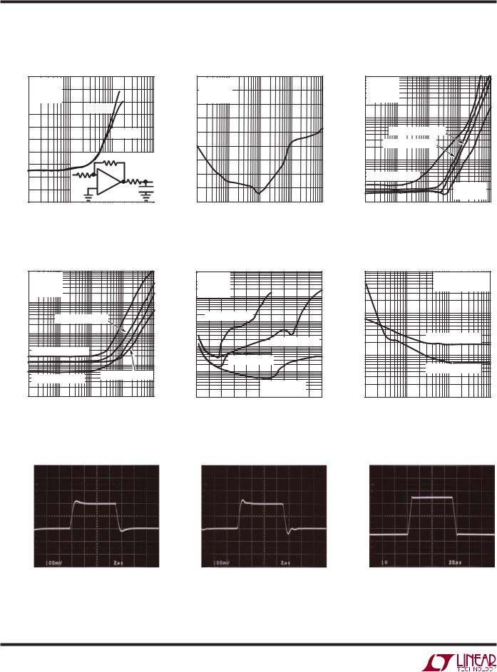
Supply Current vs Supply Voltage |
Supply Current vs Temperature |
SUPPLY CURRENT (μA)
140 |
|
|
|
|
|
|
|
|
|
|
|
120 |
|
|
|
|
|
|
|
|
|
|
|
100 |
|
|
|
|
|
|
|
|
|
|
|
80 |
|
|
|
|
|
|
|
|
|
|
|
60 |
|
|
|
|
|
|
|
|
|
|
|
40 |
|
|
|
|
|
|
|
|
|
|
|
|
|
|
|
|
|
20 |
|
PER AMPLIFIER |
|||
|
|
VCM = 0.5V |
|||
|
|
|
|||
|
|
|
TA = 25°C |
||
0 |
0.5 |
1 |
1.5 |
2 |
2.5 |
3 |
3.5 |
4 |
4.5 |
5 |
0 |
TOTAL SUPPLY VOLTAGE (V)
SUPPLY CURRENT (μA)
140 


 PER AMPLIFIER
VCM = 0.5V
130
120
VS = 5V 110 

VS = 2.5V
100
90 –55–40–25–10 5 20 35 50 65 80 95 110125
TEMPERATURE (°C)
60845 G10 |
60845 G11 |
GAIN (dB)
Open-Loop Gain vs Frequency |
CMRR vs Frequency |
100 |
|
|
90 |
|
|
80 |
|
PHASE |
70 |
|
|
|
|
|
60 |
|
|
50 |
|
|
40 |
|
|
30 |
GAIN |
|
20 |
|
|
|
|
|
10 |
|
|
0 |
|
|
–10 |
|
|
–20 |
VS = 5V |
|
–30 |
|
|
VS = 2.5V |
|
|
–40 |
|
|
1k |
10k |
100k |
FREQUENCY (Hz)
CL = 5pF |
100 |
|
|
120 |
VS = 5V |
|
|
|
110 |
||
RL = 10k |
80 |
|
|
100 |
VCM = 2.5V |
VCM = VS/2 |
|
|
RL = 1k |
||
TA = 25°C |
60 |
|
|
90 |
TA = 25°C |
|
|
|
80 |
|
|
|
|
(DEG)PHASE |
CMRR(dB) |
|
|
|
|
40 |
|
||
|
40 |
|
|
70 |
|
|
|
|
|
60 |
|
|
20 |
|
|
50 |
|
|
|
|
|
|
030
20
|
–20 |
10 |
|
|
|
|
|
|
0 |
|
|
|
|
1M |
–40 |
–10 |
10k |
100k |
1M |
10M |
10M |
1k |
|||||
|
|
|
|
FREQUENCY (Hz) |
|
|
|
60845 G12 |
|
|
|
|
60845 G13 |
PSRR (dB)
|
PSRR vs Frequency |
|
|
|
|
|
|
|
|
|
|||||||||||||||||||||
100 |
|
|
|
|
|
|
|
|
|
|
|
|
|
|
|
|
|
|
|
|
|
|
|
|
|
|
|
|
|
|
|
90 |
|
|
|
|
|
|
|
|
|
|
|
|
|
|
|
|
|
|
|
|
|
|
|
|
VS = 5V |
|
|||||
|
|
|
|
|
|
|
|
|
|
|
|
|
|
|
|
|
|
|
|
|
|
VCM = 2.5V |
|
||||||||
|
|
|
|
|
|
|
|
|
|
|
|
|
|
|
|
|
|
|
|
|
|
||||||||||
80 |
|
|
|
|
|
|
|
|
|
|
|
|
|
|
|
|
|
|
|
|
|
|
|
TA = 25°C |
|
||||||
|
|
|
|
|
|
|
|
|
|
|
|
|
|
|
|
|
|
|
|
|
|
||||||||||
70 |
|
|
|
|
|
|
|
|
|
|
|
|
|
|
|
|
|
|
|
|
|
|
|
|
|
|
|
|
|
|
|
|
|
|
|
|
|
|
|
|
|
|
|
|
|
|
|
|
|
|
|
|
|
|
|
|
|
|
|
|
|
|
|
60 |
|
|
|
|
|
|
|
|
|
|
|
|
|
|
|
|
|
|
|
|
|
|
|
|
|
|
|
|
|
|
|
|
|
|
|
|
|
|
|
|
|
|
|
|
|
|
|
|
|
|
|
|
|
|
|
|
|
|
|
|
|
|
|
50 |
|
|
|
|
|
|
|
|
|
|
|
|
|
|
|
|
|
|
|
|
|
|
|
|
|
|
|
|
|
|
|
|
|
|
|
|
|
|
|
|
|
|
|
|
|
|
|
|
|
|
|
|
|
|
|
|
|
|
|
|
|
|
|
40 |
|
|
|
|
|
|
|
|
|
|
|
|
|
|
|
|
|
|
|
|
|
|
|
|
|
|
|
|
|
|
|
|
|
|
|
|
|
|
|
|
|
|
|
|
|
|
|
|
|
|
|
|
|
|
|
|
|
|
|
|
|
|
|
30 |
|
|
|
|
|
|
|
|
|
|
|
|
|
|
|
|
|
|
|
|
|
|
|
|
|
|
|
|
|
|
|
|
|
|
|
|
|
|
|
|
|
|
|
|
|
|
|
|
|
|
|
|
|
|
|
|
|
|
|
|
|
|
|
20 |
|
|
|
|
|
|
|
|
|
|
|
|
|
|
|
|
|
|
|
|
|
|
|
|
|
|
|
|
|
|
|
|
|
|
|
|
|
|
|
|
|
|
|
|
|
|
|
|
|
|
|
|
|
|
|
|
|
|
|
|
|
|
|
10 |
|
|
|
|
|
|
|
|
|
|
|
|
|
|
|
|
|
|
|
|
|
|
|
|
|
|
|
|
|
|
|
|
|
|
|
|
|
|
|
|
|
|
|
|
|
|
|
|
|
|
|
|
|
|
|
|
|
|
|
|
|
|
|
0 |
|
|
|
|
|
|
|
|
|
|
|
|
|
|
|
|
|
|
|
|
|
|
|
|
|
|
|
|
|
|
|
|
|
|
|
|
|
|
|
|
|
|
|
|
|
|
|
|
|
|
|
|
|
|
|
|
|
|
|
|
|
|
|
–10 |
|
|
|
|
|
|
|
|
|
|
|
|
|
|
|
|
|
|
|
|
|
|
|
|
|
|
|
|
|
|
|
|
|
|
|
|
1k |
10k |
100k |
|
1M |
10M |
|||||||||||||||||||||
100 |
|
|
|
|
|
||||||||||||||||||||||||||
FREQUENCY (Hz)
60845 G14
|
Disabled Output Impedance |
Output Impedance vs Frequency |
vs Frequency |
10000 |
VS = 5V |
|
|
|
|
|
|
1000 |
|
|
|
VS = 5V |
|
||
|
|
|
|
|
|
|
|
|
|
|
|
|
|||
|
1000 |
VCM = 2.5V |
|
|
|
|
|
|
|
|
|
|
VCM = 1V |
||
|
TA = 25°C |
|
|
|
|
|
|
|
|
|
|
AV = 1 |
|
||
(Ω) |
100 |
|
|
|
|
|
|
|
(kΩ) |
100 |
|
|
|
TA = 25°C |
|
|
|
|
|
|
|
|
|
|
|
|
|
OVERSHOOT(%) |
|||
IMPEDANCEOUTPUT |
10 |
|
AV |
= 10 |
|
|
|
|
IMPEDANCEOUTPUT |
1 |
|
|
|
|
|
|
|
|
|
|
|
|
|
|
|
|
|
|
|||
|
|
|
|
|
AV = 2 |
|
|
|
|
|
|
|
|
||
|
|
|
|
|
AV = 1 |
|
|
10 |
|
|
|
|
|
||
|
1 |
|
|
|
|
|
|
|
|
|
|
|
|
|
|
|
0.1 |
|
|
|
|
|
|
|
|
|
|
|
|
|
|
|
0.01 |
|
|
|
|
|
|
|
|
|
|
|
|
|
|
|
0.001 |
|
1k |
10k |
100k |
1M |
10M |
100M |
|
0.1 |
1k |
10k |
100k |
1M |
10M |
|
100 |
|
100 |
||||||||||||
|
|
|
|
FREQUENCY (Hz) |
|
|
|
|
|
FREQUENCY (Hz) |
|
|
|||
|
|
|
|
|
|
|
60845 G15 |
|
|
|
|
|
60845 G16 |
||
Capacitive Load Handling
40
VS = 5V
35VCM = 2.5V AV = 1
30 |
|
RS = 10Ω |
25 |
– |
RS |
20 |
+ |
RS = 50Ω |
CL |
||
15 |
|
|
10
5
0
10 100 1000 CAPACITIVE LOAD (pF)
60845 G17
60845fa
7
LTC6084/LTC6085
TYPICAL PERFORMANCE CHARACTERISTICS
OVERSHOOT (%)
|
Capacitive Load Handling |
|
||
50 |
VS = 5V |
|
|
|
45 |
|
|
|
|
VCM = 2.5V |
|
|
||
40 |
AV = –1 |
|
RS = 10Ω |
|
35 |
|
|
|
|
|
|
|
|
|
30 |
|
|
RS = 50Ω |
|
25 |
|
|
||
|
|
|
|
|
20 |
|
|
1k |
|
|
|
|
|
|
15 |
|
|
|
|
10 |
|
|
– |
RS |
|
|
|
1k |
|
5 |
|
|
+ |
CL |
0 |
10 |
100 |
1000 |
10000 |
|
||||
|
|
CAPACITIVE LOAD (pF) |
|
|
|
|
|
|
60845 G18 |
CHANNEL SEPARATION (dB)
Channel Separation vs Frequency
–90
VS = 5V –95 VCM = 2.5V
TA = 25°C
–100
–105
–110
–115
–120
–125
–130
–135 0.001 0.01 0.1 1 10
FREQUENCY (MHz)
60845 G19
Total Harmonic Distortion and
Noise vs Frequency
|
1 |
|
|
|
|
|
VS = 3V |
|
|
|
|
|
VCM = 1.5V |
|
|
|
|
|
RL = 10k |
|
|
|
|
(%) |
0.1 |
|
|
|
|
NOISE |
|
AV = –2, VIN = 1VP-P |
|
|
|
|
AV = 2, VIN = 1VP-P |
|
|
||
AND |
|
|
|
||
|
|
|
|
|
|
THD |
0.01 |
|
|
|
|
|
|
|
|
|
|
|
AV = 1, VIN = 2VP-P |
|
|
|
|
|
|
|
|
AV = 1, |
|
|
0.001 |
|
|
VIN = 1VP-P |
|
|
0.1 |
1 |
10 |
100 |
|
|
0.01 |
||||
FREQUENCY (kHz)
60845 G20
Total Harmonic Distortion and
Noise vs Frequency
|
1 |
|
|
|
|
|
VS = 5V |
|
|
|
|
|
VCM = 2.5V |
|
|
|
|
|
RL = 10k |
|
|
|
|
(%) |
0.1 |
|
|
|
|
|
AV |
= 2, VIN = 1VP-P |
|
||
NOISE |
|
|
|||
0.01 |
|
|
|
|
|
AND |
|
|
|
|
|
AV = –2, VIN = 1VP-P |
|
|
|||
THD |
|
|
|||
0.001 |
|
|
|
|
|
|
|
|
|
|
|
|
AV = 1, VIN = 2VP-P |
AV = 1, VIN = 1VP-P |
|||
0.0001 |
0.1 |
1 |
10 |
100 |
|
|
0.01 |
||||
FREQUENCY (kHz)
60845 G21
THD AND NOISE (%)
Total Harmonic Distortion and
Noise vs Output Voltage
10
 RL = 10k VCM = VS/2
1 AV = 1
VS = 3V AT 20kHz
0.1
VS = 5V AT 20kHz
0.01
VS = 3V AT 1kHz
0.001
VS = 5V AT 1kHz
0.0001 

 0 0.5 1 1.5 2 2.5 3 3.5 4 4.5 5
OUTPUT VOLTAGE (VP-P)
60845 G22
THD AND NOISE (%)
Total Harmonic Distortion and
Noise vs Load Resistance
0.1
AV = 1 VCM = VS/2 AT 1kHz
0.01
VS = 3V, VIN = 1VP-P
0.001
VS = 5V, VIN = 2VP-P
0.0001
0.1 1 10 100 LOAD RESISTANCE TO GROUND (kΩ)
60845 G23
Small Signal Response |
Small Signal Response |
Large Signal Response |
100mV/DIV |
100mV/DIV |
1V/DIV |
2μs/DIV |
|
2μs/DIV |
|
20μs/DIV |
VS = 5V |
60845 G24 |
VS = 5V |
60845 G25 |
VS = 5V |
AV = 1 |
|
AV = 1 |
|
AV = 1 |
RL = ∞ |
|
RL = ∞ |
|
RL = ∞ |
|
|
CL = 220pF |
|
|
60845 G26
60845fa
8
LTC6084/LTC6085
TYPICAL PERFORMANCE CHARACTERISTICS
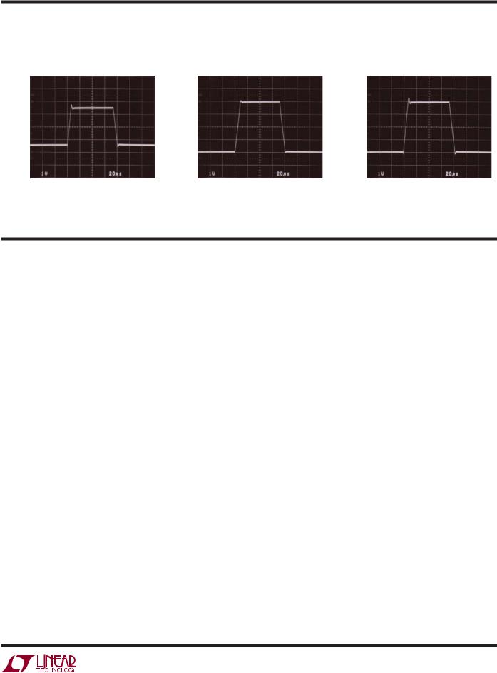
Large Signal Response |
Large Signal Response |
Large Signal Response |
1V/DIV |
1V/DIV |
1V/DIV |
20μs/DIV |
|
20μs/DIV |
|
VS = 5V |
20μs/DIV |
VS = 5V |
60845 G27 |
VS = 5V |
60845 G28 |
60845 G29 |
|
AV = –1 |
|
AV = 1 |
|
AV = –1 |
|
RL = 1k |
|
RL = ∞ |
|
RL = 1k |
|
PIN FUNCTIONS
OUT: Amplifier Output.
–IN: Inverting Input.
+IN: Noninverting Input.
V+: Positive Supply.
V–: Negative Supply.
SHDNA: Shutdown Pin of Amplifier A, active low and only available with the LTC6084DD. An internal current source pulls the pin to V+ when floating.
SHDNB: Shutdown Pin of Amplifier B, active low and only available with the LTC6084DD. An internal current source pulls the pin to V+ when floating.
NC: Not Internally Connected.
Exposed Pad: Connected to V–.
60845fa
9
LTC6084/LTC6085
APPLICATIONS INFORMATION
|
|
OUT |
NO SOLDER MASK |
NO LEAKAGE |
LTC6084 |
OVER THE GUARD RING |
CURRENT |
IN– |
|
R |
|
|
|
IN+ |
LEAKAGE |
|
|
CURRENT |
|
|
|
GUARD |
V– |
|
RING |
60845 F01 |
|
|
|
OUT |
R |
LTC6084 |
R |
IN– |
|
|
VIN |
|
|
IN+ |
GND


 V–
V–
60845 F02
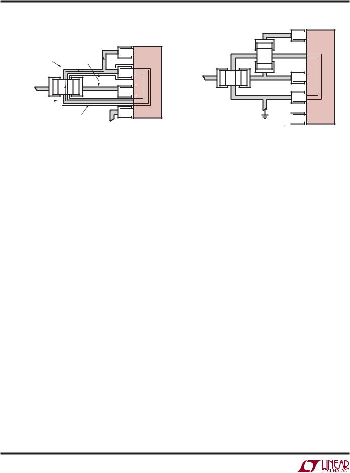
Figure 1. Sample Layout. Unity-Gain Configuration. Using Guard Ring to Shield High Impedance Input from Board Leakage
Figure 2. Sample Layout. Inverting Gain Configuration. Using Guard Ring to Shield High Impedance Input from Board Leakage
Rail-to-Rail Input
TheinputstageofLTC6084/LTC6085combinesbothPMOS and NMOS differential pairs, extending its input common mode voltage to both positive and negative supply voltages. At high input common mode range, NMOS pair is on. At low common mode range, the PMOS pair is on. The transition happens when the common voltage is between 1.3 and 0.9V below the positive supply.
Achieving Low Input Bias Current
The DD and DHC packages are leadless and make contact to the PCB beneath the package. Solder flux used during the attachment of the part to the PCB can create leakage current paths and can degrade the input bias current performance of the part. All inputs are susceptible because the backside paddle is connected to V– internally. As the input voltage or V– changes, a leakage path can be formed and alter the observed input bias current. For lowest bias current use the LTC6084/LTC6085 in the leaded MSOP/GN package. With fine PCB design rules, you can also provide a guard ring around the inputs.
Forexample,inhighsourceimpedanceapplicationssuchas pH probes, photo diodes, strain gauges, etc., the low input bias current of these parts requires a clean board layout to minimize additional leakage current into a high impedance signalnode.Amere100GΩofPCboardresistancebetween a 5V supply trace and input trace near ground potential adds 50pA of leakage current. This leakage is far greater
than the bias current of the operational amplifier. A guard ring around the high impedance input traces driven by a low impedance source equal to the input voltage prevents such leakage problems. The guard ring should extend as far as necessary to shield the high impedance signal from any and all leakage paths. Figure 1 shows the use of a guard ring in a unity-gain configuration. In this case the guard ring is connected to the output and is shielding the high impedance noninverting input from V–. Figure 2 shows the inverting gain configuration.
Rail-to-Rail Output
The output stage of the LTC6084/LTC6085 swings within 5mV of the supply rails when driving high impedance loads, in other words when no DC load current is present. See the Typical Performance Characteristics for curves of output swing versus load current. The class AB design of the output stage enables the op amp to supply load currents which are much greater than the quiescent supply current. For example, the room temperature short-circuit current is typically 12.5mA.
Capacitive Load
LTC6084/LTC6085candriveacapacitiveloadupto300pFin unity gain. The capacitive load driving capability increases as the amplifier is used in higher gain configurations. A small series resistance between the output and the load further increases the amount of capacitance the amplifier can drive.
60845fa
10