

бакМИТ_КП2015 / Компоненты по вариантам / Операционные_усилители / LTC6084HMS8
.pdfLTC6084/LTC6085
APPLICATIONS INFORMATION
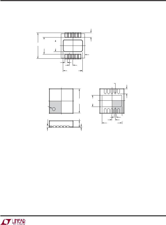
SHDN Pins
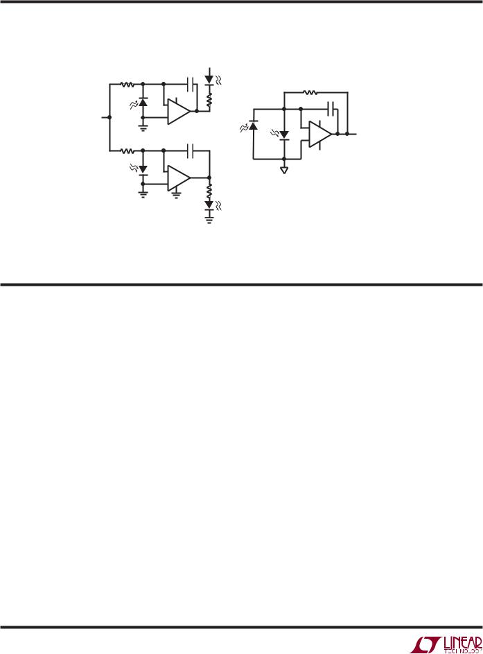
Pins 5 and 6 are used for power shutdown of the LTC6084 in the DD package. If they are floating, internal current sources pull pins 5 and 6 to V+ and the amplifiers operate normally. In shutdown the amplifier output is high impedance, and each amplifier draws less than 1μA current. This feature allows the part to be used in muxed output applications as shown in Figure 3.
10k |
10k |
|
|
5V |
|
|
|
|
|
5V |
|
|
+ |
|
LTC6084 |
|
|
A |
|
10k |
|
(DD PACKAGE) |
|
– |
|
||
INA |
SHDN |
||
|
|
A |
|
|
|
10k |
|
10k |
+ |
|
OUT |
5V |
|
||
|
|
||
10k |
|
B |
|
10k |
|
|
|
– |
|
|
|
INB |
|
SEL = 5V, OUT = –INA |
|
|
|
|
|
|
|
|
SEL = 0V, OUT = –INB |
|
|
10k |
|
|
5V |
SHDN |
|
|
|
||
SEL |
|
|
B |
|
|
|
|
|
FAIRCHILD |
|
|
|
NC7SZ04 OR |
|
|
|
EQUIVALENT |
60845 F03 |
|
Figure 3. Inverting Amplifier with Muxed Output
ESD
The LTC6084/LTC6085 has reverse-biased ESD protection diodes on all inputs and outputs as shown in the Simplified Schematic. If these pins are forced beyond either supply, unlimited current will flow through these diodes. If the current is transient and limited to 100mA or less, no damage to the device will occur.
The amplifier input bias current is the leakage current of these ESD diodes. This leakage is a function of the temperature and common mode voltage of the amplifier, as shown in the Typical Performance Characteristics.
Noise
In the frequency region above 1kHz, the LTC6084/LTC6085 shows good noise voltage performance. In this region, noisecanbedominatedbythetotalsourceresistanceofthe particular application. Specifically, these amplifiers exhibit the noise of a 58k resistor, meaning it is desirable to keep the source and feedback resistance at or below this value, i.e., RS + RG||RFB ≤ 58k. Above this total source impedance, the noise voltage is dominated by the resistors.
At low frequency, noise current can be estimated from the expression in = √2qIB, where q = 1.6 • 10–19 coulombs. Equating √4kTR f and R√2qIB f shows that for a source
resistor below 50GΩ the amplifier noise is dominated by the source resistance. Noise current rises with frequency. See the curve Input Noise Current vs Frequency in the Typical Performance Characteristics section.
60845fa
11
LTC6084/LTC6085
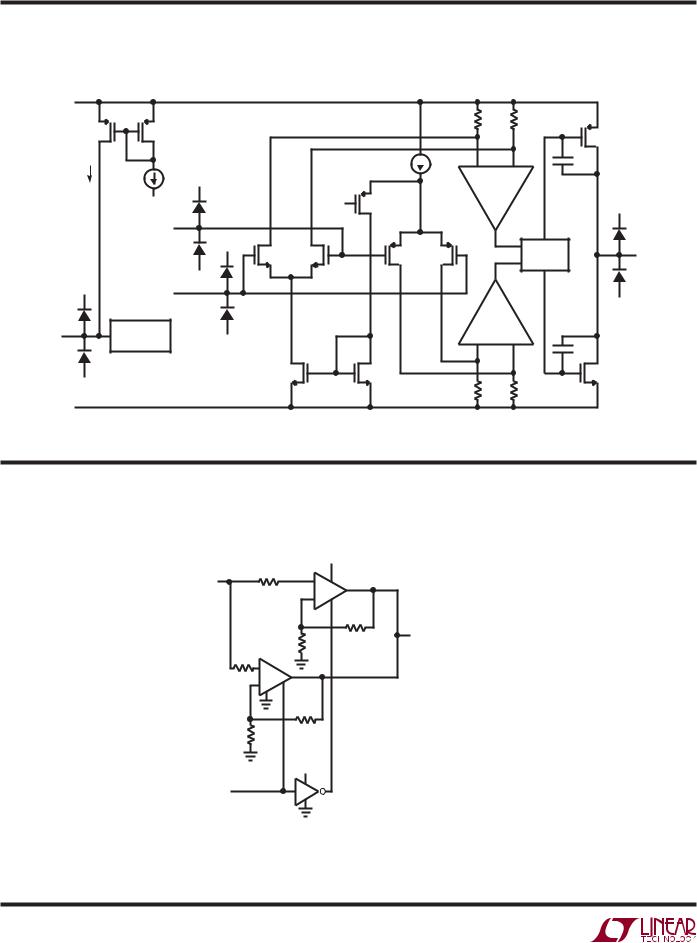
SIMPLIFIED SCHEMATIC
Simplified Schematic of the Amplifier
V+
|
|
|
|
R1 |
|
R2 |
M10 |
M11 |
|
|
|
|
M8 |
|
|
|
|
|
|
|
|
|
|
|
I1 |
|
C1 |
1μA |
I2 |
|
V+ |
|
– |
+ |
|
V– |
|
VBIAS |
M5 |
|
A1 |
|
D4 |
|
V+ |
|
+IN |
|
|
|
|
|
|
|
D7 |
|
|
|
V+ |
|
|
|
|
|
|
|
|
D3 |
|
M6 |
M7 |
|
OUTPUT |
OUT |
|
|
|
M1 |
M2 |
|
|||||
|
|
|
|
CONTROL |
|||||
|
|
|
V– D6 |
|
|
|
|
|
|
|
V+ |
|
|
|
|
|
|
D8 |
|
|
|
|
|
|
|
|
|
|
|
|
–IN |
|
|
|
|
|
|
|
V– |
|
D2 |
|
D5 |
|
|
|
|
|
|
|
|
|
|
|
|
A2 |
|
||
SHDN |
BIAS |
|
V– |
|
|
|
– |
+ |
|
GENERATION |
|
|
|
|
C2 |
||||
|
|
|
|
|
|
||||
|
D1 |
|
|
|
|
|
|
|
|
|
|
|
|
|
|
|
|
|
NOTE: SHDN IS ONLY AVAILABLE |
M3 |
M4 |
M9 |
V– IN THE DFN PACKAGE |
|
R3 |
R4 |
|
|
||
V– |
|
|
60845 SS |
TYPICAL APPLICATIONS
Gain Selectable Amplifier
|
|
|
5V |
VIN |
10k |
+ |
|
|
A |
||
|
|
– |
|
|
|
SHDNA |
|
|
|
|
4.02k |
|
|
1k |
VOUT |
|
|
|
|
10k |
+ |
B |
|
|
– |
|
|
|
SHDNB |
|
|
|
|
|
|
|
|
24.3k |
|
|
1k |
|
|
|
|
5V |
SEL = 5V, GAIN = 25 |
|
|
SEL = 0V, GAIN = 5 |
|
|
|
|
|
SEL |
|
|
A, B: LTC6084 in DFN10 |
|
|
|
FAIRCHILD NC7SZ04 OR EQUIVALENT
60845 TA02
60845fa
12
LTC6084/LTC6085
PACKAGE DESCRIPTION
DD Package
10-Lead Plastic DFN (3mm × 3mm)
(Reference LTC DWG # 05-08-1699)
0.675 ±0.05
3.50 ±0.05 |
|
|
|
|
|
|
|
|
|
|
|
|
|
|
|
1.65 ±0.05 |
|||
2.15 ±0.05 |
(2 SIDES) |
|||
|
|
PACKAGE |
|
|
|
|
OUTLINE |
|
|
0.25 ± 0.05 |
0.50 |
|
|
|
|
|
|
|
|
|
BSC |
|
|
|
|
2.38 ±0.05 |
|
|
|
|
(2 SIDES) |
|
|
|
RECOMMENDED SOLDER PAD PITCH AND DIMENSIONS |
|
|
||
|
|
|
R = 0.115 |
0.38 ± 0.10 |
|
|
|
TYP |
|
|
|
|
|
|
|
|
|
6 |
10 |
|
3.00 ±0.10 |
1.65 ± 0.10 |
|
|
|
(4 SIDES) |
(2 SIDES) |
|
|
PIN 1 |
|
|
|
|
TOP MARK |
|
|
|
|
(SEE NOTE 6) |
|
|
|
(DD) DFN 1103 |
|
|
|
|
|
|
|
|
5 |
1 |
0.200 REF |
0.75 ±0.05 |
|
|
0.25 ± 0.05 |
|
|
|
|
0.50 BSC |
|
|
|
2.38 ±0.10 |
|
|
0.00 – 0.05 |
(2 SIDES) |
|
|
|
|
|
||
|
|
BOTTOM VIEW—EXPOSED PAD |
||
NOTE:
1.DRAWING TO BE MADE A JEDEC PACKAGE OUTLINE M0-229 VARIATION OF (WEED-2). CHECK THE LTC WEBSITE DATA SHEET FOR CURRENT STATUS OF VARIATION ASSIGNMENT
2.DRAWING NOT TO SCALE
3.ALL DIMENSIONS ARE IN MILLIMETERS
4.DIMENSIONS OF EXPOSED PAD ON BOTTOM OF PACKAGE DO NOT INCLUDE
MOLD FLASH. MOLD FLASH, IF PRESENT, SHALL NOT EXCEED 0.15mm ON ANY SIDE
5.EXPOSED PAD SHALL BE SOLDER PLATED
6.SHADED AREA IS ONLY A REFERENCE FOR PIN 1 LOCATION ON THE TOP AND BOTTOM OF PACKAGE
60845fa
13
LTC6084/LTC6085 |
|
|
|
|
|
|
PACKAGE DESCRIPTION |
|
|
|
|
||
|
|
DHC Package |
|
|
|
|
|
|
16-Lead Plastic DFN (5mm × 3mm) |
|
|
|
|
|
|
(Reference LTC DWG # 05-08-1706) |
|
|
|
|
|
|
0.65 ±0.05 |
|
|
|
|
3.50 ±0.05 |
1.65 ±0.05 |
|
|
|
|
|
2.20 ±0.05 |
|
|
|
|
|
|
(2 SIDES) |
|
|
|
|
|
|
|
|
PACKAGE |
|
|
|
|
|
|
OUTLINE |
|
|
|
|
|
|
0.25 ± 0.05 |
|
|
|
|
|
|
0.50 BSC |
|
|
|
|
|
|
4.40 ±0.05 |
|
|
|
|
|
|
(2 SIDES) |
|
|
|
|
|
RECOMMENDED SOLDER PAD PITCH AND DIMENSIONS |
|
|
|
|
|
|
|
5.00 ±0.10 |
|
R = 0.115 |
0.40 |
± 0.10 |
|
|
|
TYP |
|||
|
|
(2 SIDES) |
|
|
|
|
|
|
9 |
16 |
|
|
|
|
|
|
|
|
||
|
|
|
R = 0.20 |
|
|
|
|
|
|
TYP |
|
|
|
|
|
3.00 ±0.10 |
1.65 ± 0.10 |
|
|
|
|
|
(2 SIDES) |
(2 SIDES) |
|
|
|
|
PIN 1 |
|
|
|
PIN 1 |
|
|
TOP MARK |
|
|
|
NOTCH |
|
(SEE NOTE 6) |
|
|
|
(DHC16) DFN 1103 |
||
|
|
|
8 |
1 |
||
|
|
|
|
|
||
|
0.200 REF |
0.75 ±0.05 |
|
0.25 ± 0.05 |
|
|
|
|
|
|
0.50 BSC |
|
|
|
|
|
|
4.40 ±0.10 |
|
|
|
|
0.00 – 0.05 |
(2 SIDES) |
|
|
|
|
|
|
|
|
||
|
|
|
BOTTOM VIEW—EXPOSED PAD |
|
|
|
NOTE:
1.DRAWING PROPOSED TO BE MADE VARIATION OF VERSION (WJED-1) IN JEDEC PACKAGE OUTLINE MO-229
2.DRAWING NOT TO SCALE
3.ALL DIMENSIONS ARE IN MILLIMETERS
4.DIMENSIONS OF EXPOSED PAD ON BOTTOM OF PACKAGE DO NOT INCLUDE
MOLD FLASH. MOLD FLASH, IF PRESENT, SHALL NOT EXCEED 0.15mm ON ANY SIDE
5.EXPOSED PAD SHALL BE SOLDER PLATED
6.SHADED AREA IS ONLY A REFERENCE FOR PIN 1 LOCATION ON THE TOP AND BOTTOM OF PACKAGE
60845fa
14
LTC6084/LTC6085
PACKAGE DESCRIPTION
MS8 Package
8-Lead Plastic MSOP
(Reference LTC DWG # 05-08-1660)
0.889 ± 0.127
(.035 ± .005)
|
5.23 |
|
|
|
|
|
|
|
|
|
|
|
|
|
|
|
|
|
|
|
|
|
|
|
|
|
|
|
|
|
|
|
|
|
|
|
|
|
|
|
|
|
|
|
|
|
|
|
|
|
|
|||||
|
|
|
|
|
|
|
|
|
|
|
|
|
|
|
|
3.20 – 3.45 |
|
|
|
|
|
|
|
|
|
|
|
|
|
|
|
|
|
|
|
|
|
|
|
|
|
|
|
|||||||||||||
(.206) |
|
|
|
|
|
|
|
|
|
|
|
|
|
|
|
|
|
|
|
|
|
|
|
|
|
|
|
|
|
|
|
|
|
|
|
|
|
|
|
|
|
|
|
|
||||||||||||
|
|
|
|
|
|
|
|
|
|
|
|
|
|
|
|
|
(.126 – .136) |
|
|
|
|
|
|
|
|
|
|
|
|
|
|
|
|
|
|
|
|
|
|
|
|
|
|
|||||||||||||
|
|
|
|
MIN |
|
|
|
|
|
|
|
|
|
|
|
|
|
|
|
|
|
|
|
|
|
|
|
|
|
|
|
|
|
|
|
|
|
|
|
|
|
|
|
|
|
|
||||||||||
|
|
|
|
|
|
|
|
|
|
|
|
|
|
|
|
|
|
|
|
|
|
|
|
|
|
|
|
|
|
|
3.00 ± 0.102 |
|
|
|
|
|
|
|
|
|
|
|
|
|
0.52 |
|
|
|||||||||
|
|
|
|
|
|
|
|
|
|
|
|
|
|
|
|
|
|
|
|
|
|
|
|
|
|
|
|
|
|
|
|
|
|
|
|
|
|
|
|
|
|
|
|
|
|
|||||||||||
|
|
|
|
|
|
|
|
|
|
|
|
|
|
|
|
|
|
|
|
|
|
|
|
|
|
|
|
|
|
|
|
|
|
|
|
|
|
|
|
|
|
|
|
|
|
|||||||||||
0.42 ± 0.038 |
|
|
|
|
|
|
|
|
|
|
|
|
0.65 |
|
|
|
(.118 ± .004) |
|
|
|
|
|
|
|
|
|
|
|
|
|
|
|
||||||||||||||||||||||||
|
|
|
|
|
|
|
|
|
|
|
|
|
|
|
|
|
|
|
|
|
(NOTE 3) |
|
|
|
|
|
|
|
|
|
|
(.0205) |
|
|
||||||||||||||||||||||
(.0165 ± .0015) |
|
|
|
|
|
|
|
|
|
|
|
|
|
(.0256) |
|
|
|
|
|
|
8 |
|
7 |
6 |
5 |
|
|
|
|
|||||||||||||||||||||||||||
|
|
TYP |
|
|
|
|
|
|
|
|
|
|
|
|
|
|
|
|
BSC |
|
|
|
|
|
|
|
|
|
|
|
|
|
|
|
|
|
|
|
|
|
REF |
|||||||||||||||
|
|
RECOMMENDED SOLDER PAD LAYOUT |
|
|
|
|
|
|
|
|
|
|
|
|
|
|
|
|
|
|
|
|
|
|
|
|
|
|
|
|||||||||||||||||||||||||||
|
|
|
|
|
|
|
|
|
|
|
|
|
|
|
|
|
|
|
|
|
|
|
|
|
|
|
|
|
||||||||||||||||||||||||||||
|
|
|
|
|
|
|
|
|
|
|
|
|
|
|
|
|
|
|
|
|
|
|
|
|
|
|
|
|
|
|
|
|
|
|
|
|
|
|
|
|
|
|
|
|
|
|
|
|
|
|
3.00 ± |
|
0.102 |
|
||
|
|
|
|
|
|
|
|
|
|
|
|
|
|
|
|
|
|
|
|
|
|
|
|
|
|
|
|
|
|
|
4.90 ± 0.152 |
|
|
|
|
|
|
|
|
|
|
|
|
|
|
|
||||||||||
|
|
|
|
|
|
|
|
|
|
|
|
|
|
|
|
DETAIL “A” |
|
|
|
|
|
|
|
|
|
|
|
|
|
|
(.118 ± .004) |
|
||||||||||||||||||||||||
|
|
|
|
|
|
|
|
|
0.254 |
|
|
|
(.193 ± .006) |
|
|
|
|
|
|
|
|
|
|
|
|
|
|
|||||||||||||||||||||||||||||
|
|
|
|
|
|
|
|
|
|
|
|
|
|
|
|
|
|
|
|
|
|
|
|
|
|
|
|
|
|
|
|
|
|
|
|
|
|
|
|
(NOTE 4) |
||||||||||||||||
|
GAUGE PLANE |
(.010) |
|
|
|
|
|
|
|
|
|
0° – 6° TYP |
|
|
|
|
|
|
|
|
|
|
|
|
|
|
|
|
|
|
|
|
|
|||||||||||||||||||||||
|
|
|
|
|
|
|
|
|
|
|
|
|
|
|
|
|
|
|
|
|
|
|
|
|
|
|
|
|
|
|
|
|
|
|
|
|
||||||||||||||||||||
|
|
|
|
|
|
|
|
|
|
|
|
|
|
|
|
|
|
|
|
|
|
|
|
|
|
|
|
|
|
|
|
|
|
|
|
|
|
|
|
|
|
|
|
|
|
|
|
|
||||||||
|
|
|
|
|
|
|
|
|
|
|
|
|
|
|
|
|
|
|
|
|
|
|
|
|
|
|
|
|
|
|
|
|
|
|
|
|
|
|
|
|
|
|
|
|
|
|
|
|
||||||||
|
|
|
|
|
|
|
|
|
|
|
|
|
|
|
|
|
|
|
|
|
|
|
|
|
|
|
|
|
|
|
|
|
|
|
|
|
|
|
|
|
|
|
|
|
|
|
|
|
||||||||
|
|
|
|
|
|
|
|
|
|
|
|
|
|
|
|
|
|
|
|
|
|
|
|
|
|
|
|
0.53 ± 0.152 |
|
1.10 |
1 |
|
2 |
3 |
4 |
|
|
0.86 |
|
|
||||||||||||||||
|
|
|
|
|
|
|
|
|
|
|
|
|
|
|
|
|
|
|
|
|
|
|
|
|
|
|
|
|
|
|
|
|
|
|
|
|
|
|||||||||||||||||||
|
|
|
|
|
|
|
|
|
|
|
|
|
|
|
|
|
|
|
|
|
|
|
|
|
|
|
|
|
|
|
|
|
|
|
|
|
|
|
|
|
|
|
||||||||||||||
|
|
|
|
|
|
|
|
|
|
|
|
|
|
|
(.021 ± |
.006) |
(.043) |
|
|
|
|
|
|
|
|
|
(.034) |
|
|
|||||||||||||||||||||||||||
|
|
|
|
|
|
|
|
|
|
|
|
|
|
|
|
|
|
DETAIL “A” |
|
|
|
|
|
|
|
|
|
|
|
|
||||||||||||||||||||||||||
|
|
|
|
|
|
|
|
|
|
|
|
|
|
|
|
|
|
|
|
|
|
|
MAX |
|
|
|
|
|
|
|
|
|
|
|
REF |
|||||||||||||||||||||
0.18 |
|
|
|
|
|
|
|
|
|
|
|
|
|
|
|
|
|
|
|
|
|
|
|
|
|
|
|
|
|
|
|
|
|
|
|
|
|
|
|
|
|
|
|
|
|
|
|
|
|
|
|
|
|
|
||
|
|
|
|
|
|
|
|
|
|
|
|
|
|
|
|
|
|
|
|
|
|
|
|
|
|
|
|
|
|
|
|
|
|
|
|
|
|
|
|
|
|
|
|
|
|
|
|
|
|
|
|
|
||||
|
|
|
|
|
|
|
|
|
|
|
|
|
|
|
|
|
|
|
|
|
|
|
|
|
|
|
|
|
|
|
|
|
|
|
|
|
|
|
|
|
|
|
|
|
|
|
|
|
|
|
|
|
||||
|
|
|
|
|
|
|
|
|
|
|
|
|
|
|
|
|
|
|
|
|
|
|
|
|
|
|
|
|
|
|
|
|
|
|
|
|
|
|
|
|
|
|
|
|
|
|
|
|
|
|
|
|
|
|
|
|
|
|
(.007) |
|
|
|
|
|
|
|
|
|
|
|
|
|
|
|
|
|
|
|
|
|
|
|
|
|
|
SEATING |
|
|
|
|
|
|
|
|
|
|
|
|
|
|
|
|
|
|
|
|
|
|
|
|
|
|
|
|
|
|
|
|
|
|
|
|
|
|
|
|
|
|
|
|
|
|
|
|
|
|
|
|
|
|
|
|
|
PLANE |
|
0.22 – 0.38 |
|
|
|
|
|
|
|
|
|
|
|
|
|
0.1016 ± 0.0508 |
||||||||||
|
|
|
|
|
|
|
|
|
|
|
|
|
|
|
|
|
|
|
|
|
|
|
|
|
|
|
|
|
|
|
|
(.009 – .015) |
|
|
|
|
|
|
|
|
|
|
|
(.004 ± .002) |
||||||||||||
|
|
|
|
|
|
|
|
|
|
|
|
|
|
|
|
|
|
|
|
|
|
|
|
|
|
|
|
|
|
|
|
0.65 |
|
|
|
|
|
|||||||||||||||||||
|
|
|
|
|
|
|
|
|
|
|
|
|
|
|
|
|
|
|
|
|
|
|
|
|
|
|
|
|
|
|
|
|
TYP |
|
|
|
|
|
|
MSOP (MS8) 0307 REV F |
||||||||||||||||
|
|
NOTE: |
|
|
|
|
|
|
|
|
|
|
|
|
|
|
|
|
|
|
|
|
|
|
|
|
|
|
|
|
|
|
|
(.0256) |
|
|
|
|
|
|
|
|
|
|
|
|||||||||||
|
|
|
|
|
|
|
|
|
|
|
|
|
|
|
|
|
|
|
|
|
|
|
|
|
|
|
|
|
|
|
|
|
|
|
BSC |
|
|
|
|
|
|
|
|
|
|
|
||||||||||
|
|
1. DIMENSIONS IN MILLIMETER/(INCH) |
|
|
|
|
|
|
|
|
|
|
|
|
|
|
|
|
|
|
|
|
|
|
|
|||||||||||||||||||||||||||||||
|
|
|
|
|
|
|
|
|
|
|
|
|
|
|
|
|
|
|
|
|
|
|
|
|
|
|
|
|
||||||||||||||||||||||||||||
2.DRAWING NOT TO SCALE
3.DIMENSION DOES NOT INCLUDE MOLD FLASH, PROTRUSIONS OR GATE BURRS.
MOLD FLASH, PROTRUSIONS OR GATE BURRS SHALL NOT EXCEED 0.152mm (.006") PER SIDE
4.DIMENSION DOES NOT INCLUDE INTERLEAD FLASH OR PROTRUSIONS.
INTERLEAD FLASH OR PROTRUSIONS SHALL NOT EXCEED 0.152mm (.006") PER SIDE
5.LEAD COPLANARITY (BOTTOM OF LEADS AFTER FORMING) SHALL BE 0.102mm (.004") MAX
GN Package
16-Lead Plastic SSOP (Narrow .150 Inch)
(Reference LTC DWG # 05-08-1641)
|
|
|
|
|
|
|
|
|
|
|
|
|
|
|
.045 ± .005 |
|
|||||||||||||||||
|
|
|
|
|
|
|
|
|
|
|
|
|
|
|
|
|
|
|
|
|
|
|
|
|
|
|
|
|
|
|
|
|
|
|
|
|
|
|
|
|
|
|
|
|
|
|
|
|
|
|
|
|
|
|
|
|
|
|
|
|
|
|
|
|
|
|
|
|
|
|
|
|
|
|
|
|
|
|
|
|
|
|
|
|
|
|
|
|
|
|
|
|
|
|
|
|
|
|
|
|
|
|
|
|
|
|
|
|
|
|
|
|
|
|
|
|
|
|
|
|
|
|
|
|
|
|
|
|
|
|
|
|
|
|
|
|
|
|
|
|
|
|
|
|
|
|
|
|
|
|
|
|
|
||||||||||||||||
.254 MIN |
|
|
|
|
|
|
|
|
|
.150 – .165 |
|
||||||||||||||||||||||
|
|
|
|
|
|
|
|
|
|
|
|
|
|
|
|
|
|
|
|
|
|
|
|
|
|
|
|
|
|
|
|
|
|
|
|
|
|
|
|
|
|
|
|
|
|
|
|
|
|
|
|
|
|
|
|
|
|
|
|
|
|
|
|
|
|
|
|
|
|
|
|
|
|
|
|
|
|
|
|
|
|
|
|
|
|
|
|
|
|
|
|
|
|
|
|
|
|
|
|
|
|
|
|
|
|
|
|
|
|
|
|
|
|
|
|
|
|
|
|
|
|
|
|
|
|
|
|
|
|
|
|
|
|
|
|
.0165 ± .0015 |
|
|
|
|
|
|
|
|
|
|
|
|
|
|
|
|
|
.0250 BSC |
|
||||||||||||||
|
RECOMMENDED SOLDER PAD LAYOUT |
|
|||||||||||||||||||||||||||||||
|
|
|
|
|
|
|
|
|
|
|
|
|
|
|
|
|
|
|
|
|
|
|
|
|
|
|
.015 ± .004 |
× 45° |
|||||
|
|
|
|
|
|
|
|
|
|
|
|
|
|
|
|
|
|
|
|
|
|
|
(0.38 ± 0.10) |
|
|||||||||
.007 – .0098 |
|
|
|
|
|
|
|
|
|
|
|
|
0° – 8° TYP |
|
|||||||||||||||||||
|
|
|
|
|
|
|
|
|
|
|
|
||||||||||||||||||||||
(0.178 – 0.249) |
|
|
|
|
|
|
|
|
|
|
|
|
|
|
|
|
|
|
|
||||||||||||||
|
|
|
|
|
|
|
|
|
|
|
|
|
|
|
|
|
|
|
|
|
|
|
|
|
|||||||||
|
|
|
|
|
|
|
|
|
|
|
|
|
|
|
|
|
|
|
|
|
|
|
|
|
|||||||||
|
|
|
|
|
|
|
|
|
|
|
|
|
|
|
|
|
|
|
|
|
|
|
|
|
|
|
|
|
|
|
|
|
|
|
|
|
|
|
|
|
|
|
|
|
|
.016 – .050 |
|
|
|
|
|
||||||||||||||||
|
|
|
|
|
|
|
|
|
|
|
|
|
|
|
|
||||||||||||||||||
|
|
|
|
|
|
|
|
|
|
|
|
||||||||||||||||||||||
|
|
|
|
|
|
|
|
|
(0.406 – 1.270) |
|
|
|
|
||||||||||||||||||||
NOTE: |
|
|
|
|
|
|
|
|
|
|
|
|
|
|
|
|
|
|
|
||||||||||||||
1. CONTROLLING DIMENSION: INCHES |
|
||||||||||||||||||||||||||||||||
2. DIMENSIONS ARE IN |
|
INCHES |
|
||||||||||||||||||||||||||||||
(MILLIMETERS) |
|
|
|||||||||||||||||||||||||||||||
3. DRAWING NOT TO SCALE
*DIMENSION DOES NOT INCLUDE MOLD FLASH. MOLD FLASH SHALL NOT EXCEED 0.006" (0.152mm) PER SIDE
**DIMENSION DOES NOT INCLUDE INTERLEAD FLASH. INTERLEAD FLASH SHALL NOT EXCEED 0.010" (0.254mm) PER SIDE
|
|
|
|
|
|
|
|
|
|
|
|
|
.189 – .196* |
|
|
|
|
|
|
|
|
|
|
|
|
|
||||
|
|
|
|
|
|
|
|
|
|
|
|
|
|
|
|
|
|
|
|
|
|
|
|
|
||||||
|
|
|
|
|
|
|
|
|
|
|
|
|
(4.801 – 4.978) |
|
|
|
|
|
.009 |
|
|
|
||||||||
|
|
|
|
|
|
|
|
|
|
|
|
|
|
|
|
|
|
|
|
|
|
|
|
|
||||||
|
|
|
|
|
|
|
|
|
16 |
15 |
14 |
13 |
12 |
11 |
10 9 |
(0.229) |
|
|||||||||||||
|
|
|
|
|
|
|
|
|
|
|
|
REF |
||||||||||||||||||
|
|
|
|
|
|
|
|
|
|
|
|
|
|
|
|
|
|
|
|
|
|
|
|
|
|
|
|
|
|
|
|
|
|
|
|
|
|
|
|
|
|
|
|
|
|
|
|
|
|
|
|
|
|
|
|
|
|
|
|
|
|
|
|
|
|
|
|
|
|
|
|
|
|
|
|
|
|
|
|
|
|
|
|
|
|
|
|
|
|
|
|
|
|
|
|
|
|
|
|
|
|
|
|
|
|
|
|
|
|
|
|
|
|
|
|
|
|
|
|
|
|
|
|
.229 |
– .244 |
|
|
|
|
|
|
|
|
|
|
|
|
|
|
|
|
|
|
|
.150 – .157** |
|||||||||
|
|
|
|
|
|
|
|
|
|
|
|
|
|
|
|
|
|
|
|
|
|
|
|
|
|
|
|
|||
(5.817 |
– 6.198) |
|
|
|
|
|
|
|
|
|
|
|
|
|
|
|
(3.810 – 3.988) |
|||||||||||||
|
|
|
|
|
|
|
|
|
|
|
|
|
|
|
|
|
|
|
|
|
|
|
|
|
|
|
|
|
|
|
|
|
|
|
|
|
|
|
|
|
|
|
|
|
|
|
|
|
|
|
|
|
|
|
|
|
|
|
|
|
|
|
|
|
|
|
|
|
|
|
|
|
|
|
|
|
|
|
|
|
|
|
|
|
|
|
|
|
|
|
|
|
|
|
|
|
|
|
|
|
|
|
|
|
|
|
|
|
|
|
|
|
|
|
|
|
|
|
|
|
|
|
|
|
|
|
|
|
|
|
|
|
|
|
|
|
|
|
|
|
|
|
|
|
|
|
|
|
|
|
|
|
|
|
|
|
|
|
|
|
|
|
|
|
|
|
|
|
|
|
|
|
|
|
|
|
|
|
|
|
|
|
|
|
|
|
|
|
|
|
|
1 |
2 |
3 |
4 |
5 |
6 |
7 |
8 |
|
|
|
|
|
|
|
|
|
||||||||
|
|
|
.0532 |
– .0688 |
|
|
|
|
|
|
|
|
|
|
|
|
.004 – .0098 |
|||||||||||||
|
|
|
(1.35 |
– 1.75) |
|
|
|
|
|
|
|
|
|
|
|
|
(0.102 – 0.249) |
|
|
|||||||||||
|
|
|
|
|
|
|
|
|
|
|
|
|
|
|
|
|
|
|
|
|
|
|
|
|
|
|
|
|
|
|
|
|
|
|
|
|
|
|
|
|
|
|
|
|
|
|
|
|
|
|
|
|
|
|
|
|
|
|
|
|
|
|
|
|
|
|
|
|
|
|
|
|
|
|
|
|
|
|
|
|
|
|
|
|
|
|
|
|
|
|
|
|
|
.008 |
– .012 |
|
|
|
|
|
|
|
|
|
|
|
|
.0250 |
|
|
|
GN16 (SSOP) 0204 |
|||||||||||
|
|
|
|
|
|
|
|
|
|
|
|
|
|
|
|
|||||||||||||||
(0.203 |
– 0.305) |
|
|
|
|
|
|
|
|
(0.635) |
|
|
|
|
|
|
|
|
|
|||||||||||
|
|
TYP |
|
|
|
|
|
|
|
|
|
|
|
|
|
BSC |
|
|
|
|
|
|
|
|
|
|||||
60845fa
Information furnished by Linear Technology Corporation is believed to be accurate and reliable. |
15 |
However, no responsibility is assumed for its use. Linear Technology Corporation makes no representa- |
|
tion that the interconnection of its circuits as described herein will not infringe on existing patent rights. |
LTC6084/LTC6085
TYPICAL APPLICATION
Bipolar Analog Isolation Amplifier
VCC
1M |
|
10pF |
|
|
|
1% |
|
|
|
|
|
|
OC1 |
|
|
|
|
|
|
|
1M |
|
|
|
VCC |
|
|
||
|
|
|
3pF |
||
OC1 |
– |
2k |
|
|
|
|
|
|
|||
|
|
|
|
||
VIN |
+ |
1/2 LTC6084 |
|
+5V |
|
|
|
OC1 |
– |
|
|
|
|
|
VOUT = VIN |
||
1M |
|
10pF |
OC2 |
+ |
|
|
|
LTC6240HV |
|||
1% |
|
|
|||
|
|
|
|||
|
|
|
|
–5V |
|
OC2 |
– 1/2 LTC6084 |
GNDB |
|
|
|
|
+ |
2k |
BW ≈ 40kHz, EITHER POLARITY |
||
GNDA |
|
LARGE SIGNAL TRANSITION DELAY ≈ 50μs |
|||
|
|
||||
|
|
OC2 |
SMALL SIGNAL DEAD ZONE: |VIN| ≤ 10mV |
||
|
|
|
|
|
|
VCC = 5V, |
|
OC1, OC2: AVAGO TECHNOLOGIES HCNR201 |
VOUT = ±5V, |
||
VIN = ±5V |
|
www.avagotech.com |
|
RELATIVE TO GNDB |
|
RELATIVE TO GNDA
60845 TA03
RELATED PARTS
PART NUMBER |
DESCRIPTION |
COMMENTS |
|
|
|
LTC6078/LTC6079 |
Dual/Quad Micropower Precision Rail-to-Rail Op Amps |
25μV VOS(MAX), 0.7μV/°C VOS Drift(MAX), 1pA IBIAS(MAX) |
LTC6081/LTC6082 |
Dual/Quad Precision Rail-to-Rail Input/Output Amps |
70μV VOS(MAX), 0.8μV/°C VOS Drift(MAX), 1pA IBIAS(MAX) |
LTC6087/LTC6088 |
Dual/Quad 14MHz Rail-to-Rail Input/Output Amps |
750μV VOS(MAX), 5μV/°C VOS Drift(MAX), 1pA IBIAS |
LTC6240/LTC6241/ |
Single/Dual/Quad Low Noise Rail-to-Rail Output Op Amps |
7nV/√Hz Noise, 0.2pA IBIAS, 18MHz Gain Bandwidth |
LTC6242 |
|
|
LTC6244 |
Dual Low Noise Rail-to-Rail Output Op Amps |
8nV/√Hz Noise, 1pA IBIAS, 50MHz Gain Bandwidth |
16 Linear Technology Corporation
1630 McCarthy Blvd., Milpitas, CA 95035-7417
60845fa
LT 0209 REV A • PRINTED IN USA
(408) 432-1900 ● FAX: (408) 434-0507 ● www.linear.com |
♥ LINEAR TECHNOLOGY CORPORATION 2008 |