

MAX11162 |
16-Bit, 500ksps, +5V Unipolar Input, |
|
SAR ADC, in Tiny 10-Pin µMAX |
|
|
|
|
|
CS2 |
|
|
|
|
|
CS1 |
|
|
|
|
|
CONVERT |
|
CNVST |
|
|
CNVST |
DIGITAL HOST |
SDI |
MAX11162 |
SDO |
SDI |
MAX11162 |
SDO |
|
SCLK |
|
|
SCLK |
|
|
|
|
|
|
DATA IN |
|
|
|
|
|
CLK |
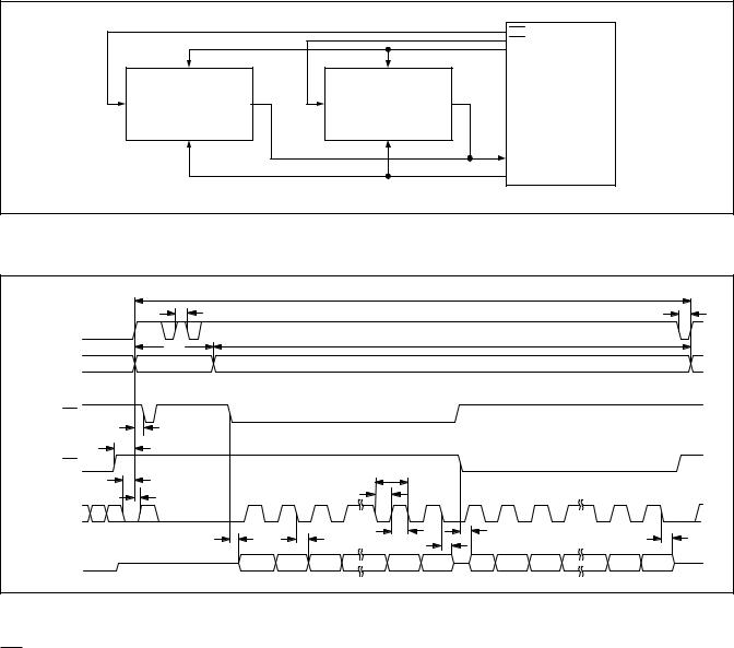
Figure 9. CS Mode 4-Wire, No-Busy Indicator Connection Diagram
|
|
|
|
|
tCYC |
|
|
|
|
|
|
|
tCNVPW |
|
|
|
|
|
|
|
|
|
tCNVPW |
CNVST |
|
|
|
|
tACQ |
|
|
|
|
|
|
|
tCONV |
|
|
|
|
|
|
|
|
|
|
|
|
|
|
|
|
|
|
|
|
|
|
ACQUISITION |
CONVERSION |
|
|
|
ACQUISITION |
|
|
|
|
|
|
SDI(CS1) |
|
|
|
|
|
|
|
|
|
|
|
tHSDICNV |
|
|
|
|
|
|
|
|
|
|
|
tSSDICNV |
|
|
|
|
|
|
|
|
|
|
|
SDI(CS2) |
|
|
|
|
tSCLK |
|
|
|
|
|
|
|
tSSCKCNV |
|
|
|
|
|
|
|
|
|
|
|
|
|
|
|
|
|
|
|
|
|
|
|
tHSCKCNV |
|
|
tSCLKL |
|
|
|
|
|
|
|
SCLK |
|
1 |
2 |
3 |
15 |
16 |
17 |
18 |
19 |
31 |
32 |
|
tEN |
|
|
tSCLKH |
|
|
|
tEN |
|
|
tDIS |
|
|
|
tDSDO |
|
tDIS |
|
|
|
|
||
|
|
|
|
|
|
|
|
|
|
|
|
SDO |
|
D15 |
D14 |
D13 |
D1 |
D0 |
D15 |
D14 |
D13 |
D1 |
D0 |
Figure 10. CS Mode 4-Wire, No-Busy Indicator Serial Interface Timing
CS Mode 4-Wire, No-Busy Indicator
The 4-wire CS mode with no-busy indicator is ideally suited for multichannel applications. In this case, the CNVST pin may be used for low-jitter simultaneous sampling while the SDI pin(s) are used to control data readback. In Figure 9, two ADCs are connected to an SPI-compatible digital host with corresponding timing given in Figure 10.
With SDI high, a rising edge on CNVST completes the acquisition, initiates the conversion, and forces SDO to high impedance. This mode requires CNVST to be held high during the conversion and data readback phases. Note that if CNVST and SDI are low, SDO is driven low.
During the conversion, the SDI pin(s) can be used as a select line for other devices on the board, but must be returned high before the minimum conversion time and held high until the maximum conversion time to avoid generating the busy signal indicator.
When the conversion is complete, the MAX11162 enters the acquisition phase. ADC data is read by driving its respective SDI line low, outputting the MSB onto SDO. The remaining data bits are then clocked by subsequent SCLK falling edges. SDO returns to high impedance after the 16th SCLK falling edge or when CNVST goes high.
www.maximintegrated.com |
Maxim Integrated │ 20 |
MAX11162 |
16-Bit, 500ksps, +5V Unipolar Input, |
|
SAR ADC, in Tiny 10-Pin µMAX |
|
|
|
CS1 |
|
|
|
CONVERT |
|
|
|
OVDD |
|
|
|
DIGITAL HOST |
|
CNVST |
|
10kΩ |
|
|
|
|
SDI |
MAX11162 |
SDO |
DATA IN |
|
SCLK |
|
IRQ |
|
|
|
CLK |
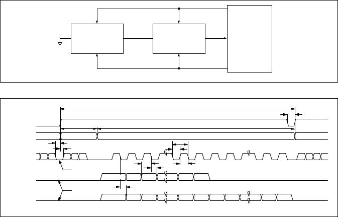
Figure 11. CS Mode 4-Wire with Busy Indicator Connection Diagram
|
|
tCYC |
|
|
|
|
|
|
|
|
|
|
tCNVPW |
CNVST |
|
|
|
|
|
|
|
tCONV |
|
|
tACQ |
|
|
ACQUISITION |
CONVERSION |
|
|
ACQUISITION |
|
|
|
tSSDICNV |
|
|
|
|
|
|
tHSDICNV |
|
|
|
|
|
SDI |
|
|
|
|
|
|
|
tSSCKCNV |
|
|
|
tSCLK |
|
|
tHSCKCNV |
|
|
tSCLKL |
|
|
SCLK |
1 |
2 |
3 |
15 |
16 |
17 |
|
|
tDSDO |
|
tSCLKH |
|
|
|
|
|
|
|
tDIS |
|
SDO |
BUSY BIT |
D15 |
D14 |
|
D1 |
D0 |
Figure 12. CS Mode 4-Wire with Busy Indicator Serial Interface Timing
CS Mode 4-Wire, With Busy Indicator
The 4-wire CS mode with busy indicator is shown in Figure 11 where a single ADC is connected to an SPI-compatible digital host with interrupt input. The corresponding timing is given in Figure 12. This mode is ideally suited for single ADC applications where the CNVST pin may be used for low-jitter sampling while the SDI pin is used for data readback.
With SDI high, a rising edge on CNVST completes the acquisition, initiates the conversion and forces SDO to high impedance. This mode requires CNVST to be held high during the conversion and data readback phases. Note that if CNVST and SDI are low, SDO is driven low. During
the conversion, the SDI pin can be used as a select line for other devices on the board, but must be returned low before the minimum conversion time and held low until the busy signal is generated.
When the conversion is complete SDO transitions from high impedance to a low logic level signaling to the digital host through the interrupt input that data readback can commence. The MAX11162 then enters the acquisition phase. The data bits are clocked out, MSB first, by subsequent SCLK falling edges. SDO returns to high impedance after the 17th SCLK falling edge or when CNVST goes high and is then pulled to OVDD through the external pullup resistor.
www.maximintegrated.com |
Maxim Integrated │ 21 |
MAX11162 |
16-Bit, 500ksps, +5V Unipolar Input, |
|
SAR ADC, in Tiny 10-Pin µMAX |
|
|
|
|
|
|
|
|
|
|
CONVERT |
|
|
CNVST |
|
|
|
|
CNVST |
|
|
DIGITAL HOST |
SDI |
MAX11162 |
SDO |
SDOA |
SDI |
MAX11162 |
SDO |
SDOB |
DATA IN |
||
|
|
|||||||||
Device A |
SCLK |
|
|
Device B |
SCLK |
|
|
|
||
|
|
|
|
|
|
|
|
|
||
|
|
|
|
|
|
|
|
|
|
CLK |
Figure 13. Daisy-Chain Mode, No-Busy Indicator Connection Diagram
|
|
|
|
|
|
tCYC |
|
|
|
|
|
|
|
|
|
|
|
|
|
|
|
|
|
|
tCNVPW |
CNVST |
tCONV |
|
|
|
|
|
tACQ |
|
|
|
|
|
|
|
|
|
|
|
|
|
|
|
|
||
ACQUISITION |
CONVERSION |
|
|
|
|
|
ACQUISITION |
|
|
|
|
|
|
tSSCKCNV |
|
|
|
|
tSCLK |
|
|
|
|
|
|
|
tHSCKCNV |
|
|
|
tSCLKL |
|
|
|
|
|
|
|
SCLK |
|
1 |
2 |
3 |
14 |
15 |
16 |
17 |
18 |
30 |
31 |
32 |
|
SELECT NO |
tSSDISCK |
|
tHSDISCK |
tSCLKH |
|
|
|
|
|
||
|
|
|
|
|
|
|
|
|
|
|||
|
BUSY |
|
|
|
|
|
|
|
|
|
||
|
|
|
|
|
|
|
|
|
|
|
|
|
SDOA = SDIB |
OUTPUT |
DA15 |
DA14 |
DA13 |
|
DA1 |
DA0 |
|
|
|
|
|
|
|
|
|
|
|
|
||||||
|
SELECT |
|
tDSDO |
|
|
|
|
|
|
|
|
|
SDOB |
CHAIN MODE |
DB15 |
DB14 |
DB13 |
|
DB1 |
DB0 |
DA15 |
DA14 |
|
DA1 |
DA0 |
|
|
|
||||||||||
|
|
|
DAISY-CHAIN MODE, NO BUSY INDICATOR SERIAL INTERFACE TIMING |
|
|
|
||||||
Figure 14. Daisy-Chain Mode, No-Busy Indicator Serial Interface Timing
Daisy-Chain Mode, No-Busy Indicator
The daisy-chain mode with no-busy indicator is ideally suited for multichannel isolated applications that require minimal wiring complexity. Simultaneous sampling of multiple ADC channels is realized on a 3-wire serial interface where data readback is analogous to clocking a shift register. In Figure 13, two ADCs are connected to an SPI-compatible digital host with corresponding timing given in Figure 14.
The daisy-chain mode is engaged when the MAX11162 detects the low state on SDI at the rising edge of CNVST. In this mode, CNVST is brought low and then high to trigger the completion of the acquisition phase and the start of a conversion. A low SCLK state on the rising edge of CNVST signals to the internal controller that the no-busy indicator will be output. When in chain mode, the SDO output is driven active at all times.
When SDI and CNVST are both low, SDO is driven low, thus engaging the daisy-chain mode of operations on the downstream MAX11162 parts. For example, in Figure 13 part A has its SDI tied low so the chain mode of operation
will be selected on every conversion. When CNVST goes low to trigger another conversion, part A’s SDO and consequently part B’s SDI go low as well. On the next CNVST rising edge both parts A and B will select the daisy-chain mode interface.
When a conversion is complete, the MSB is presented onto SDO, and the MAX11162 returns to the acquisition phase. The remaining data bits, stored within the internal shift register, are clocked out on each subsequent SCLK falling edge. The SDI input of each ADC in the chain is used to transfer conversion data from the previous ADC into the internal shift register of the next ADC, thus allowing for data to be clocked through the multichip chain on each SCLK falling edge. Each ADC in the chain outputs its MSB data first requiring 16 × N clocks to read back N ADCs.
In daisy-chain mode, the maximum conversion rate is reduced due to the increased readback time. For instance, with a 6ns digital host setup time and 3V interface, up to four MAX11162 devices running at a conversion rate of 218ksps can be daisy-chained on a 3-wire port.
www.maximintegrated.com |
Maxim Integrated │ 22 |
MAX11162 |
16-Bit, 500ksps, +5V Unipolar Input, |
|
SAR ADC, in Tiny 10-Pin µMAX |
|
|
|
|
|
|
|
|
|
|
|
|
|
|
|
CONVERT |
|
|
CNVST |
|
|
|
|
CNVST |
|
|
|
|
CNVST |
|
|
DIGITAL HOST |
SDI |
MAX11162 |
SDO |
SDOA |
SDI |
MAX11162 |
SDO |
SDOB |
SDI |
MAX11162 |
SDO |
SDOC |
DATA IN |
|||
|
|
|
|||||||||||||
Device A |
SCLK |
|
|
Device B |
SCLK |
|
|
Device C |
SCLK |
|
|
IRQ |
|||
|
|
|
|
|
|
|
|
|
|
|
|
||||
|
|
|
|
|
|
|
|
|
|
|
|
|
|
|
CLK |
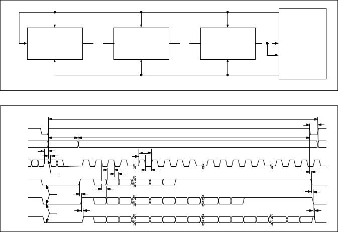
Figure 15. Daisy-Chain Mode with Busy Indicator Connection Diagram
|
|
|
|
|
|
|
|
|
|
tCYC |
|
|
|
|
|
|
|
|
|
|
|
|
|
|
|
|
|
|
|
|
|
|
|
|
|
tCNVPW |
|
CNVST = SDIA |
tCONV |
|
|
|
|
|
|
|
|
tACQ |
|
|
|
|
|
|
|
|
|
|
|
|
|
|
|
|
|
|
|
|
|
|
|
|
|
||
ACQUISITION |
CONVERSION |
|
|
|
|
tSCLK |
|
|
|
ACQUISITION |
|
|
|
|
|
|
|
|
tSSCKCNV |
tHSCKCNV |
|
|
|
|
|
|
|
|
|
|
|
|
|
|
|
|
|
|
|
|
|
tSCLKH |
|
|
|
|
|
|
|
|
|
|
|
|
|
|
SCLK |
|
1 |
2 |
3 |
4 |
15 |
16 |
17 |
18 |
19 |
31 |
32 |
33 |
34 |
35 |
47 |
48 |
49 |
|
SELECT |
tSSDISCK |
|
tHSDISCK |
|
tSCLKL |
|
|
|
|
|
|
|
|
|
tDSDOSDI |
||
|
BUSY |
|
|
|
|
|
|
|
|
|
|
|
|
|
|
|
||
|
|
|
|
|
|
|
|
|
|
|
|
|
|
|
|
|
|
|
SDOA = SDIB |
MODE |
BUSY |
DA15 |
DA14 |
DA13 |
|
DA1 |
DA0 |
|
|
|
|
|
|
|
|
|
|
|
|
|
|
|
|
|
|
|
|
|
|
|||||||
|
SELECT |
BIT |
|
tDSDO |
|
|
|
|
|
|
|
|
|
|
|
|
tDSDOSDI |
|
|
tDSDOSDI |
|
|
|
|
|
|
|
|
|
|
|
|
|||||
|
CHAIN |
|
|
|
|
|
|
|
|
|
|
|
|
|
|
|
||
SDOB = SDIC |
MODE |
BUSY |
DB15 |
DB14 |
DB13 |
|
DB1 |
DB0 |
DA15 |
DA14 |
|
DA1 |
DA0 |
|
|
|
|
|
|
SELECT |
BIT |
|
|
|
|
|
|
|
|
|
|
|
|
|
|
|
|
|
tDSDOSDI |
|
|
|
|
|
|
|
|
|
|
|
|
|
|
tDSDOSDI |
||
|
CHAIN |
|
|
|
|
|
|
|
|
|
|
|
|
|
|
|
|
|
SDOC |
MODE |
BUSY |
DC15 |
DC14 |
DC13 |
|
DC1 |
DC0 |
DB15 |
DB14 |
|
DB1 |
DB0 |
DA15 |
DA14 |
|
DA1 |
DA0 |
|
|
BIT |
|
|
|
|
|
|
|
|
|
|
|
|
|
|
|
|
Figure 16. Daisy-Chain Mode with Busy Indicator Serial Interface Timing
Daisy-Chain Mode, With Busy Indicator
The daisy-chain mode with busy indicator is shown in Figure 15 where three ADCs are connected to an SPIcompatible digital host with corresponding timing given in Figure 16.
The daisy-chain mode is engaged when the MAX11162 detects a low state on SDI at the rising edge of CNVST. Additionally, SDI can be tied directly to CNVST to trigger the chain interface mode. In this mode, CNVST is brought low and then high to trigger the completion of the acquisition phase and the start of a conversion. A high SCLK state on the rising edge of CNVST signals to the internal controller that the busy indicator will be outputted. When in daisychain mode, the SDO output is driven active at all times.
When SDI and CNVST are both low, SDO is driven low, thus engaging the daisy-chain mode of operations on the downstream MAX11162 parts. For example, in Figure 15 part A has its SDI tied low so the daisy-chain mode of oper-
ation will be selected on every conversion. When CNVST goes low to trigger another conversion, part A’s SDO and consequently part B’s SDI go low as well. The same is true on part C’s SDI input. Consequently, on the next CNVST rising edge all parts in the chain will select the daisy-chain mode interface.
When a conversion is complete, the busy indicator is presented onto each SDO, and the MAX11162 returns to the acquisition phase. As each part completes its conversion, it looks for a busy enable signal on its SDI pin from the earlier part in the chain. When it sees a busy enable signal on its input and its own conversion has completed, it enables its busy output signal on SDO. Thus the busy enable signals are propagated down the chain and the final busy enable signal at the host indicates that all devices in the chain have completed their conversion and all can be readout.
The conversion data bits are stored within the internal shift register and clocked out on each subsequent SCLK falling
www.maximintegrated.com |
Maxim Integrated │ 23 |