

MAX11162 |
16-Bit, 500ksps, +5V Unipolar Input, |
|
SAR ADC, in Tiny 10-Pin µMAX |
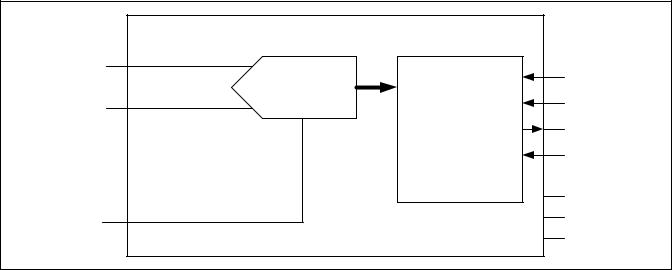
Functional Diagram
AIN+ |
SDI |
|
|
||
16-BIT ADC |
SCLK |
|
AIN- |
||
|
||
INTERFACE |
SDO |
|
AND |
||
|
||
CONTROL |
CNVST |
|
MAX11162 |
VDD |
|
|
||
REF |
OVDD |
|
|
||
|
GND |
Detailed Description
The MAX11162 is a 16-bit single-channel, pseudo-dif- ferential SAR ADC with maximum throughput rates of 500ksps. This ADC measures a unipolar input voltage interval from 0V to VREF. The external reference interval ranges from 2.5V to VDD. Both inputs, AIN+ and AIN-, are sampled with an integrated pseudo-differential track-and- hold (T/H) exhibiting no pipeline delay or latency, making this ADC ideal for multiplexed channel applications.
The MAX11162 inputs are protected for up to Q20mA of overrange current. This ADC is powered from a 4.75V to 5.25V analog supply (VDD) and a separate 2.3V to 5.25V digital supply (OVDD). The MAX11162 requires 0.5µs to acquire the input sample on an internal track-and-hold and then converts the sampled signal to 16 bits of resolution using an internally clocked converter.
Analog Inputs
The MAX11162 ADC consists of a true sampling pseudodifferential input stage with high-impedance, capacitive inputs. The internal T/H circuitry feature a small-signal bandwidth of about 6MHz to provide 16-bit accurate sampling in 0.5µs. This allows for accurate sampling of a number of scanned channels through an external multiplexer.
The MAX11162 on the AIN+ input, accurately converts input signals in the interval from AINto (VREF + AIN-).
AIN+ has a max input interval from -0.1V to (VDD + 0.1V). AINhas a max input interval from -0.1V to +0.1V.
The MAX11162 performs a true differential sampling on inputs between AIN+ and AINwith good common-mode rejection (see the Typical Operating Circuit). Connecting AINto the ground reference of the input signal source improves rejection of common-mode noise of remote transducer inputs.
www.maximintegrated.com |
Maxim Integrated │ 12 |
MAX11162
Overvoltage Input Clamps
The MAX11162 includes an input clamping circuit that activates when the input voltage at AIN+ is above (VDD + 300mV) or below -300mV. The clamp circuit remains high impedance while the input signal is within the range of -100mV to (VDD + 100mV) and draws little to no current. However, when the input signal exceeds this range the clamps begin to turn on. Consequently, to obtain the highest accuracy, ensure that the input voltage does not exceed the range of -100mV to (VDD + 100mV).
To make use of the input clamps, connect a resistor (RS) between the AIN+ input and the voltage source to limit the voltage at the analog input and to ensure the fault current into the devices does not exceed Q20mA. Note that the voltage at the AIN+ input pin limits to approximately 7V during a fault condition so the following equation can be used to calculate the value of RS:
R = VFAULT MAX −7V
S 20mA
16-Bit, 500ksps, +5V Unipolar Input, SAR ADC, in Tiny 10-Pin µMAX
where VFAULTMAX is the maximum voltage that the source produces during a fault condition.
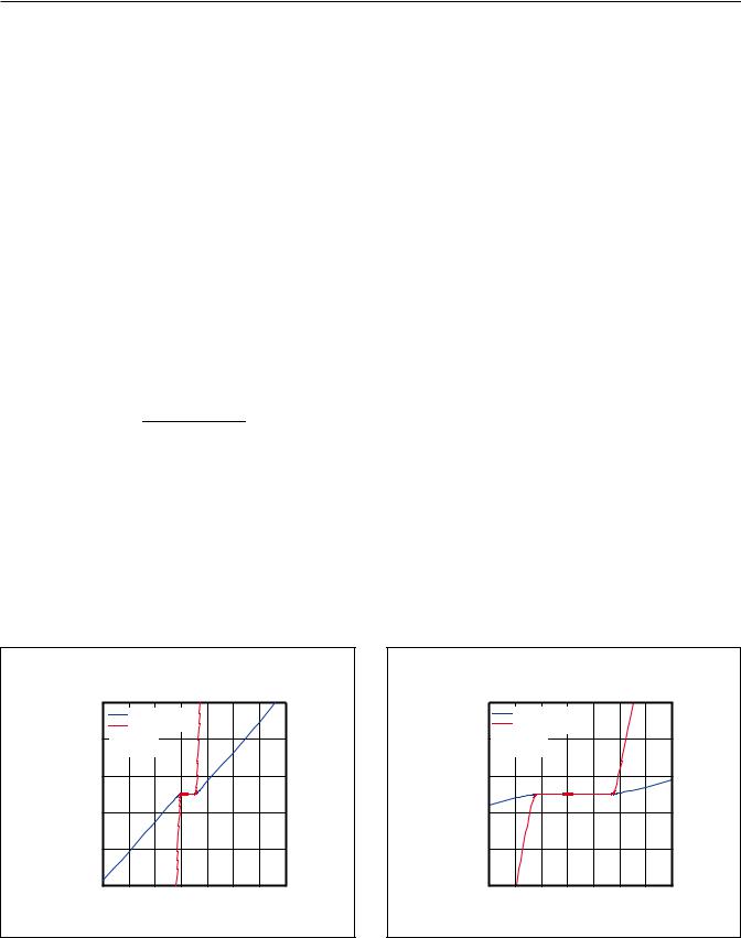
Figure 1 and Figure 2 illustrate the clamp circuit voltage current characteristics for a source impedance RS = 1170I. While the input voltage is within the -300mV to (VDD + 300mV) range, no current flows in the input clamps. Once the input voltage goes beyond this voltage range, the clamps turn on and limit the voltage at the input pin.
Reference
The MAX11162 requires a low-impedance reference source on the REF pin to support 16-bit accuracy. Maxim offers a wide range of precision references ideal for 16-bit accuracy. Table 1 lists some of the options recommended.
It is recommended that a reference buffer or the output of one of these recommended reference sources be used to drive this pin. In addition, an external bypass capacitor of at least 10µF with low inductance and ESR should be placed as close as possible to the REF pin, thus minimiz-
Table 1. MAX11162 External Reference Recommendations
PART |
VOUT (V) |
TEMPERATURE |
INITIAL |
NOISE (0.1Hz TO |
PACKAGE |
|
COEFFICIENT (MAX) |
ACCURACY (%) |
10Hz) (µVP-P) |
||||
MAX6126 |
2.5, 3, 4.096, 5.0 |
3 (A), 5 (B) |
0.06 |
1.35 |
µMAX-8 |
|
SO-8 |
||||||
|
|
|
|
|
||
|
|
|
|
|
|
|
MAX6325 |
2.5 |
1 |
0.04 |
1.5 |
SO-8 |
|
|
|
|
|
|
|
|
MAX6341 |
4.096 |
1 |
0.02 |
2.4 |
SO-8 |
MAX11162 INPUT CLAMP
CHARACTERISTICS
|
25 |
INPUT SOURCE |
|
|
|
|
||
|
|
|
|
|
|
|||
|
|
AIN+ PIN |
|
|
|
|
|
|
PIN (mA) |
15 |
RS = 1170I |
|
|
|
|
|
|
|
VDD = 5.0V |
|
|
|
|
|
||
5 |
|
|
|
|
|
|
|
|
INTO |
|
|
|
|
|
|
|
|
|
|
|
|
|
|
|
|
|
CURRENT |
-5 |
|
|
|
|
|
|
|
|
|
|
|
|
|
|
|
|
|
-15 |
|
|
|
|
|
|
|
|
-25 |
|
|
|
|
|
|
|
|
-30 |
-20 |
-10 |
0 |
10 |
20 |
30 |
40 |
|
VOLTAGE AT AIN+ PIN AND INPUT SOURCE (V) |
|||||||
Figure 1. Input Clamp Characteristics
MAX11162 INPUT CLAMP
CHARACTERISTICS
|
25 |
|
INPUT SOURCE |
|
|
|
|
||
|
|
|
|
|
|
|
|||
|
|
|
AIN+ PIN |
|
|
|
|
|
|
(mA) |
15 |
RS = 1170I |
|
|
|
|
|
||
|
VDD = 5.0V |
|
|
|
|
|
|
||
PIN |
5 |
|
|
|
|
|
|
|
|
INTO |
|
|
|
|
|
|
|
|
|
|
|
|
|
|
|
|
|
|
|
CURRENT |
-5 |
|
|
|
|
|
|
|
|
|
|
|
|
|
|
|
|
|
|
|
-15 |
|
|
|
|
|
|
|
|
|
-25 |
-4 |
-2 |
0 |
2 |
4 |
6 |
8 |
10 |
|
|
||||||||
|
|
VOLTAGE AT AIN+ PIN AND INPUT SOURCE (V) |
|||||||
Figure 2. Input Clamp Characteristics (Zoom In)
www.maximintegrated.com |
Maxim Integrated │ 13 |

MAX11162
ing the PCB inductance. X7R or X5R ceramic capacitors in a 1210 case size or smaller have been found to provide adequate bypass performance. Y5U or Z5U ceramic capacitors are not recommended due to their high voltage and temperature coefficients.
Input Amplifier
The conversion results are accurate when the ADC acquires the input signal for an interval longer than the input signal's worst-case settling time. The ADC input sampling capacitor charges during the acquisition period. During this acquisition period, the settling of the sampled voltage is affected by the source resistance and the input sampling capacitance. Sampling error can be estimated by modeling the time constant of the total input capacitance and the driving source impedance.
Although the MAX11162 is easy to drive, an amplifier buffer is recommended if the source impedance is such that when driving a switch capacitor of ~40pF a significant settling error in the desired acquisition time will occur. If this is the case, it is recommended that a configuration shown in the Typical Operating Circuit is used where at least a 4.7nF capacitor is attached to the AIN+ pin. This capacitance reduces the size of the transient at the start of the acquisition period, which in some buffers will cause an input signal dependent offset.
Regardless of whether an external buffer amp is used or
not, the time constant, RSOURCE × CLOAD, of the input should not exceed tACQ/12, where RSOURCE is the total signal source impedance, CLOAD is the total capacitance
at the ADC input (external and internal) and tACQ is the acquisition period. Thus to obtain accurate sampling in a
0.5µs acquisition time a source impedance of less than
2.1kΩ should be used if driving the ADC directly. When driving the ADC from a buffer, a series resistance (5Ω to 15Ω typical) is recommended between the amplifier and the external input capacitance as shown in the Typical Operating Circuit.
16-Bit, 500ksps, +5V Unipolar Input, SAR ADC, in Tiny 10-Pin µMAX
These amplifier features help to select the ADC driver:
1)Fast settling time: For multichannel multiplexed applications the driving operational amplifier must settle to 16-bit resolution when a full-scale step is applied during the minimum acquisition time.
2)Low noise: It is important to ensure that the driver amplifier has a low average noise density appropriate for the desired bandwidth of the application. In the case of the MAX11162, settling in a 0.5µs duration requires an RC filter bandwidth of approximately 4MHz. With this bandwidth, it is preferable to use an amplifier that will produce an output noise-spectral density of less than 4.5nV/√HZ, to ensure that the overall SNR is not degraded significantly. It is recommended to insert an external RC filter at the MAX11162 AIN+ input to attenuate out-of-band input noise and preserve the ADC's SNR. The effective RMS noise at the MAX11162 AIN+ input is 36µV, thus additional noise from a buffer circuit should be significantly lower to achieve the maximum SNR performance.
3)THD performance: The input buffer amplifier used should have better THD performance than the MAX11162 to ensure the THD of the digitized signal is not degraded.
Table 2 summarizes the operational amplifiers that are compatible with the MAX11162. The MAX9632 has sufficient bandwidth, low enough noise and distortion to support the full performance of the MAX11162. The MAX9633 is a dual amplifier and can support buffering for true pseudo-differential sampling.
Transfer Function
The ideal transfer characteristic for the MAX11162 is shown in Figure 3. The precise location of various points on the transfer function are given in Table 3.
Table 2. List of Recommended ADC Driver Op Amps for MAX11162
AMPLIFIER |
INPUT-NOISE |
SMALL-SIGNAL |
SLEW RATE |
THD |
I |
COMMENTS |
DENSITY |
BANDWIDTH |
(V/µs) |
(dB) |
CC |
||
|
(nV/√HZ) |
(MHz) |
(mA) |
|
||
|
|
|
|
|
||
|
|
|
|
|
|
|
MAX9632 |
1 |
55 |
30 |
-128 |
3.9 |
Low noise, THD at 10kHz |
MAX9633 |
3 |
27 |
18 |
-128 |
3.5 |
Low noise, dual amp, THD at 10kHz |
www.maximintegrated.com |
Maxim Integrated │ 14 |

MAX11162 |
16-Bit, 500ksps, +5V Unipolar Input, |
|
SAR ADC, in Tiny 10-Pin µMAX |
MAX11162
OUTPUT CODE (HEX)
Figure 3. Unipolar Transfer Function
|
+FS - 1LSB |
|
+FS = VREF |
FFFF |
|
|
Transition |
FFFE |
+FS |
LSB = |
|
|
65536 |
8001 |
|
8000
7FFF
7FFE
00001
00000
0 |
|
|
VREF/2 |
|
+FS |
|
|
+0.5×LSB |
|
|
+FS-1.5×LSB |
|
|
|
|
INPUT VOLTAGE (LSB)
Table 3. Transfer Function Example
CODE TRANSITION |
UNIPOLAR INPUT (V) |
DIGITAL OUTPUT CODE (HEX) |
+FS - 1.5 LSB |
4.999886 |
FFFE - FFFF |
Midscale + 0.5 LSB |
2.500038 |
8000 - 8001 |
Midscale |
2.500000 |
8000 |
Midscale - 0.5 LSB |
2.499962 |
7FFF - 8000 |
0.5 LSB |
0.000038 |
0000 - 0001 |
www.maximintegrated.com |
Maxim Integrated │ 15 |