


MAX11101
14-Bit, +5V, 200ksps ADC with 10µA Shutdown
Output Coding and Transfer Function
The data output from the MAX11101 is binary and Figure 8 depicts the nominal transfer function. Code transitions occur halfway between successive-integer LSB values (VREF = 4.096V and 1 LSB = 250FV or 4.096V/16384).
Applications Information
External Reference
The MAX11101 requires an external reference with a voltage range between 3.8V and AVDD. Connect the external reference directly to REF. Bypass REF to AGND with a 4.7FF capacitor. When not using a low-ESR bypass capacitor, use a 0.1FF ceramic capacitor in parallel with the 4.7FF capacitor. Noise on the reference degrades conversion accuracy.
The input impedance at REF is 40I for DC currents. During a conversion, the external reference at REF must deliver 100FA of DC load current and have an output impedance of 10I or less.
For optimal performance, buffer the reference through an op amp and bypass the REF input. Consider the MAX11101’s equivalent input noise (80FVRMS) when choosing a reference.
OUTPUT CODE
FULL-SCALE 11 . . . 111 TRANSITION
11 . . . 110
11 . . . 101
FS = VREF
1LSB = VREF 16384
00 . . . 011
00 . . . 010
00 . . . 001
00 . . . 000
0 1 2 |
3 |
FS |
|
INPUT VOLTAGE (LSB) |
FS - 3/2 LSB |
Figure 8. Unipolar Transfer Function, Full Scale (FS) = VREF, Zero Scale (ZS) = GND
Input Buffer
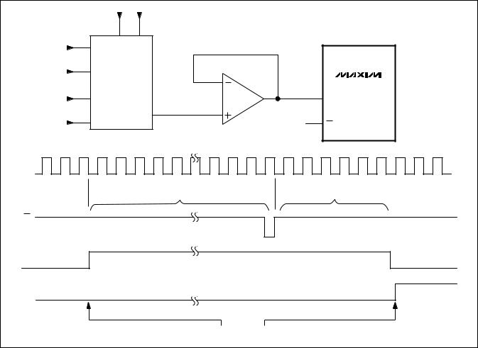
Most applications require an input buffer amplifier to achieve 14-bit accuracy. If the input signal is multiplexed, switch the input channel immediately after acquisition, rather than near the end of or after a conversion (Figure 9). This allows the maximum time for the input buffer amplifier to respond to a large step change in the input signal. The input amplifier must have a slew rate of at least 2V/Fs to complete the required output voltage change before the beginning of the acquisition time.
At the beginning of the acquisition, the internal sampling capacitor array connects to AIN (the amplifier output), causing some output disturbance. Ensure that the sampled voltage has settled before the end of the acquisition time.
Digital Noise
Digital noise can couple to AIN and REF. The conversion clock (SCLK) and other digital signals active during input acquisition contribute noise to the conversion result. Noise signals synchronous with the sampling interval result in an effective input offset. Asynchronous signals produce random noise on the input, whose high-frequency components may be aliased into the frequency band of interest. Minimize noise by presenting a low impedance (at the frequencies contained in the noise signal) at the inputs. This requires bypassing AIN to AGND, or buffering the input with an amplifier that has a small-signal bandwidth of several MHz, or preferably both. AIN has about 4MHz of bandwidth.
Distortion
Avoid degrading dynamic performance by choosing an amplifier with distortion much less than the MAX11101’s total harmonic distortion (THD = -99dB at 1kHz) at frequencies of interest. If the chosen amplifier has insufficient common-mode rejection, which results in degraded THD performance, use the inverting configuration (positive input grounded) to eliminate errors from this source. Low temperature-coefficient, gain-setting resistors reduce linearity errors caused by resistance changes due to self-heating. To reduce linearity errors due to finite amplifier gain, use amplifier circuits with sufficient loop gain at the frequencies of interest.
DC Accuracy
To improve DC accuracy, choose a buffer with an offset much less than the MAX11101’s offset (1mV (max) for +5V supply), or whose offset can be trimmed while maintaining stability over the required temperature range.


 Maxim Integrated Products 12
|
|
|
MAX11101 |
14-Bit, +5V, 200ksps ADC with 10µA Shutdown |
|||
IN1 |
A0 |
A1 |
|
|
|
|
|
IN2 |
4-TO-1 |
|
|
|
MUX |
|
MAX11101 |
|
|
|
|
IN3 |
|
|
AIN |
|
|
|
|
|
|
OUT |
|
IN4 |
|
|
CS |
CLK |
|
|
|
|
|
CONVERSION |
ACQUISITION |
CS |
|
|
|
A0 |
|
|
|
A1 |
|
|
|
|
|
|
CHANGE MUX INPUT HERE |
Figure 9. Change Multiplexer Input Near Beginning of Conversion to Allow Time for Slewing and Settling
Serial Interfaces
The MAX11101’s interface is fully compatible with SPI, QSPI, and MICROWIRE standard serial interfaces.
If a serial interface is available, establish the CPU’s serial interface as master, so that the CPU generates the serial clock for the MAX11101. Select a clock frequency between 100kHz and 4.8MHz:
1)Use a general-purpose I/O line on the CPU to pull CS low.
2)Activate SCLK for a minimum of 24 clock cycles. The serial data stream of eight leading zeros followed by the MSB of the conversion result begins at the falling edge of CS. DOUT transitions on SCLK’s falling edge and the output is available in MSB-first format.
Observe the SCLK to DOUT valid timing characteristic. Clock data into the FP on SCLK’s rising edge.
3)Pull CS high at or after the 24th falling clock edge. If CS remains low, trailing zeros are clocked out after the 2 sub-bits, S1 and S0.
4)With CS high, wait at least 50ns (tCSW) before starting a new conversion by pulling CS low. A conversion can be aborted by pulling CS high before the conversion ends. Wait at least 50ns before starting a new conversion.
Data can be output in three 8-bit sequences or continuously. The bytes contain the results of the conversion padded with eight leading zeros before the MSB. If the serial clock has not been idled after the sub-bits (S1 and S0) and CS has been kept low, DOUT sends trailing zeros.


 Maxim Integrated Products 13

MAX11101
14-Bit, +5V, 200ksps ADC with 10µA Shutdown
I/O |
CS |
SCK |
SCLK |
MISO |
DOUT |
SPI |
VDD |
|
|
|
MAX11101 |
SS |
|
Figure 10a. SPI Connections
I/O |
CS |
SK |
SCLK |
SI |
DOUT |
MICROWIRE |
|
|
MAX11101 |
Figure 10b. MICROWIRE Connections
SPI and MICROWIRE Interfaces
When using the SPI (Figure 10a) or MICROWIRE (Figure 10b) interfaces, set CPOL = 0 and CPHA = 0. Conversion begins with a falling edge on CS (Figure 10c). Three consecutive 8-bit readings are necessary to obtain the entire 14-bit result from the ADC. DOUT data transitions on the serial clock’s falling edge. The first 8-bit data stream contains all leading zeros. The second 8-bit data stream contains the MSB through D6. The third 8-bit data stream contains D5 through D0 followed by S1 and S0.
|
|
|
|
1ST BYTE READ |
|
|
|
|
|
|
|
|
|
2ND BYTE READ |
|
|
|
|
||
SCLK |
|
1 |
|
|
4 |
|
6 |
8 |
|
|
|
|
|
|
12 |
|
|
|
16 |
|
|
|
|
|
|
|
|
|
|
|
|
|
|
|
|
|
|
|
|
|
|
CS |
|
|
|
|
|
|
|
|
|
|
|
|
|
|
|
|
|
|
|
|
DOUT* |
0 |
0 |
0 |
0 |
0 |
0 |
0 |
0 |
|
|
|
D13 |
D12 |
D11 |
D10 |
D9 |
D8 |
D7 |
D6 |
D5 |
|
|
|
|
|
|
|
|
|
|
|
||||||||||
|
|
|
|
|
|
|
|
|
|
|
|
MSB |
|
|
|
|
|
|
|
|
*WHEN CS IS HIGH, DOUT = HIGH-Z |
|
|
|
|
|
|
|
|
|
|
|
|
|
|
|
|
|
|
|
|
|
|
|
|
|
|
|
|
|
3RD BYTE READ |
|
|
|
|
|
|
|
|
|
|
|
|
|
|
|
|
|
|
|
|
20 |
|
|
|
24 |
|
|
|
|
|
|
|
|
|
|
|
|
|
D5 |
D4 |
D3 |
D2 |
D1 |
D0 |
S1 |
S0 |
|
HIGH-Z |
|
|
|
|
|
|
|
|
|
|
|
|
|
|
|
|
|
|
||||||||
|
|
|
|
|
|
|
|
|
|
|
LSB |
|
|
|
|
|
|
|
|
|
Figure 10c. SPI/MICROWIRE Interface Timing Sequence (CPOL = CPHA =0)


 Maxim Integrated Products 14

MAX11101
14-Bit, +5V, 200ksps ADC with 10µA Shutdown
|
CS |
|
|
|
CS |
|
|
|
|
|
|
||||||
SCK |
|
SCLK |
|
|
||||
MISO |
|
DOUT |
|
|
||||
QSPI |
VDD |
|
|
|||||
|
|
|
|
|
|
|
|
|
|
|
|
|
|
|
|
|
|
MAX11101
SS
Figure 11a. QSPI Connections
SCLK |
1 |
4 |
6 |
8 |
|
|
12 |
|
|
|
16 |
|
|
|
20 |
|
|
|
24 |
|
CS |
|
|
|
|
|
|
|
|
|
|
|
|
|
|
|
|
|
|
|
|
|
|
|
END OF |
|
|
|
|
|
|
|
|
|
|
|
|
|
|
|
|
HIGH-Z |
DOUT* |
|
ACQUISITION |
D13 |
D12 |
D11 |
D10 |
D9 |
D8 |
D7 |
D6 |
D5 |
D4 |
D3 |
D2 |
D1 |
D0 |
S1 |
S0 |
||
|
|
|||||||||||||||||||
|
|
|
|
|||||||||||||||||
*WHEN CS IS HIGH, DOUT = HIGH-Z |
|
|
MSB |
|
|
|
|
|
|
|
|
|
|
|
|
LSB |
|
|
|
|
|
|
|
|
|
|
|
|
|
|
|
|
|
|
|
|
|
|
|
||
Figure 11b. QSPI Interface Timing Sequence (CPOL = CPHA = 0)
VDD |
VDD |
SCLK |
SCK |
DOUT |
SDI |
CS |
I/O |
|
PIC16/17 |
MAX11101 |
|
GND |
|
Figure 12a. SPI Interface Connection for a PIC16/PIC17
QSPI Interface
Using the high-speed QSPI interface with CPOL = 0 and
CPHA = 0, the MAX11101 supports a maximum fSCLK of 4.8MHz. Figure 11a shows the MAX11101 connected
to a QSPI master and Figure 11b shows the associated interface timing.
PIC16 with SSP Module and PIC17 Interface
The MAX11101 is compatible with a PIC16/PIC17 microcontroller (FC) using the synchronous serial-port (SSP) module.
To establish SPI communication, connect the controller as shown in Figure 12a. Configure the PIC16/PIC17 as system master, by initializing its synchronous serial-port control register (SSPCON) and synchronous serial-port status register (SSPSTAT) to the bit patterns shown in Table 1 and Table 2.
In SPI mode, the PIC16/PIC17 FC allows 8 bits of data to be synchronously transmitted and received simultaneously. Three consecutive 8-bit readings (Figure 12b) are necessary to obtain the entire 14-bit result from the ADC. DOUT data transitions on the serial clock’s falling edge and is clocked into the FC on SCLK’s rising edge. The first 8-bit data stream contains all zeros. The second 8-bit data stream contains the MSB through D6. The third 8-bit data stream contains bits D5 through D0 followed by S1 and S0.


 Maxim Integrated Products 15

|
|
|
|
|
|
|
|
|
|
|
|
|
|
|
|
|
MAX11101 |
|||
14-Bit, +5V, 200ksps ADC with 10µA Shutdown |
||||||||||||||||||||
|
|
|
|
1ST BYTE READ |
|
|
|
|
|
|
|
|
|
2ND BYTE READ |
|
|
|
|
||
SCLK |
|
|
|
|
|
|
|
|
|
|
|
|
|
|
12 |
|
|
|
16 |
|
|
|
|
|
|
|
|
|
|
|
|
|
|
|
|
|
|
|
|
|
|
CS |
|
|
|
|
|
|
|
|
|
|
|
|
|
|
|
|
|
|
|
|
DOUT* |
0 |
0 |
0 |
0 |
0 |
0 |
0 |
0 |
|
|
|
D13 |
D12 |
D11 |
D10 |
D9 |
D8 |
D7 |
D6 |
D5 |
|
|
|
|
|
|
|
|
|
|
|
||||||||||
|
|
|
|
|
|
|
|
|
|
|
|
MSB |
|
|
|
|
|
|
|
|
*WHEN CS IS HIGH, DOUT = HIGH-Z |
|
|
|
|
|
|
|
|
|
|
|
|
|
|
|
|
|
|
|
|
|
|
|
|
|
|
|
|
|
3RD BYTE READ |
|
|
|
|
|
|
|
|
|
|
|
|
|
|
|
|
|
|
|
|
20 |
|
|
|
24 |
|
|
|
|
|
|
|
|
|
|
|
|
|
D5 |
D4 |
D3 |
D2 |
D1 |
D0 |
S1 |
S0 |
|
HIGH-Z |
|
|
|
|
|
|
|
|
|
|
|
|
|
|
|
|
|
|
||||||||
|
|
|
|
|
|
|
|
|
|
|
LSB |
|
|
|
|
|
|
|
|
|
Figure 12b. SPI Interface Timing with PIC16/PIC17 in Master Mode (CKE = 1, CKP = 0, SMP = 0, SSPM3 - SSPM0 =0001) |
||||||||||||||||||||
Table 1. Detailed SSPCON Register Contents
CONTROL BIT |
MAX11101 |
SYNCHRONOUS SERIAL-PORT CONTROL REGISTER (SSPCON) |
||
SETTINGS |
||||
|
|
|
||
|
|
|
|
|
WCOL |
BIT 7 |
X |
Write Collision Detection Bit |
|
|
|
|
|
|
SSPOV |
BIT 6 |
X |
Receive Overflow Detect Bit |
|
|
|
|
|
|
|
|
|
Synchronous Serial-Port Enable Bit: |
|
SSPEN |
BIT 5 |
1 |
0: Disables serial port and configures these pins as I/O port pins. |
|
|
|
|
1: Enables serial port and configures SCK, SDO, and SCI pins as serial port pins. |
|
|
|
|
|
|
CKP |
BIT 4 |
0 |
Clock Polarity Select Bit. CKP = 0 for SPI master mode selection. |
|
|
|
|
|
|
SSPM3 |
BIT 3 |
0 |
|
|
|
|
|
|
|
SSPM2 |
BIT 2 |
0 |
Synchronous Serial-Port Mode Select Bit. Sets SPI master mode and selects fCLK = fOSC/16 |
|
|
|
|
||
SSPM1 |
BIT 1 |
0 |
||
|
||||
|
|
|
|
|
SSPM0 |
BIT 0 |
1 |
|
|
|
|
|
|
|
Table 2. Detailed SSPSTAT Register Contents
CONTROL BIT |
MAX11101 |
SYNCHRONOUS SERIAL-PORT CONTROL REGISTER (SSPSTAT) |
||
SETTINGS |
||||
|
|
|
||
|
|
|
|
|
SMP |
BIT 7 |
0 |
SPI Data Input Sample Phase. Input data is sampled at the middle of the data output time. |
|
|
|
|
|
|
CKE |
BIT 6 |
1 |
SPI Clock Edge Select Bit. Data will be transmitted on the rising edge of the serial clock. |
|
|
|
|
|
|
D/A |
BIT 5 |
X |
Data Address Bit |
|
|
|
|
|
|
P |
BIT 4 |
X |
STOP Bit |
|
|
|
|
|
|
S |
BIT 3 |
X |
START Bit |
|
|
|
|
|
|
R/W |
BIT 2 |
X |
Read/Write Bit Information |
|
|
|
|
|
|
UA |
BIT 1 |
X |
Update Address |
|
|
|
|
|
|
BF |
BIT 0 |
X |
Buffer Full Status Bit |
|
|
|
|
|
|


 Maxim Integrated Products 16