

MAX11101
14-Bit, +5V, 200ksps ADC with 10µA Shutdown
AIN |
|
|
|
|
|
|
|
|
|
|
|
|
|
|
|
|
|
|
|
|
|
|
|
|
|
|
|
|
|
|
|
|
|
|
AIN |
|
|
|
|
|
|
CS |
|
CS |
|||||
|
|
|
|
|
|
|
|
|
|
|
|
|
|
|
|
|
||||||||
VREF |
|
|
|
|
|
|
|
|
|
|
REF |
|
|
|
|
|
|
SCLK |
|
SCLK |
||||
|
|
|
|
|
|
|
|
|
|
|
|
|
|
|
|
|
||||||||
|
|
|
|
|
|
|
|
|
|
|
|
|
|
|
|
DOUT |
|
DOUT |
||||||
|
|
|
4.7µF |
|
|
|
|
|
|
|
||||||||||||||
+5V |
|
|
|
AVDD |
MAX11101 |
|
|
|
|
|||||||||||||||
|
|
|
|
|
|
|
|
|
|
|
|
|
|
|||||||||||
|
|
|
|
|
|
0.1µF |
|
|
|
|
||||||||||||||
+5V |
|
|
|
|
|
|
DVDD |
|
|
|
|
|
|
AGND |
|
|
|
|
||||||
|
|
|
|
|
|
|
|
|
|
|
|
|
|
|
|
|||||||||
|
|
|
|
|
|
|
|
|
|
|
|
|
|
|
|
|
|
|
|
|||||
|
|
|
|
|
|
|
|
|
|
|
|
|
|
|
|
|
|
|
|
|||||
|
|
|
|
|
|
|
|
|
|
|
|
|
|
|
|
|
|
|
|
|
|
|||
|
|
|
|
|
|
|
|
|
|
|
|
|
|
|
|
|
|
|
|
|
|
|||
|
|
|
|
|
|
|
|
|
|
0.1µF |
|
|
|
|
|
|
|
DGND |
|
|
|
|
||
|
|
|
|
|
|
|
|
|
|
|
|
|
|
|
|
|
|
|
|
|
||||
|
|
|
|
|
|
|
|
|
|
|
|
|
|
|
|
|
|
|
|
|
|
|
|
|
|
|
|
|
|
|
|
|
|
|
|
|
|
|
|
|
|
|
|
|
|
|
|
|
|
 GND
GND
Figure 4. Typical Operating Circuit
|
REF |
|
|
|
AIN |
TRACK |
CAPACITIVE DAC |
|
|
|
ZERO |
|||
|
|
|
||
CSWITCH |
HOLD |
CDAC 32pF |
|
|
3pF |
RIN |
|||
|
|
|||
|
GND |
|
800Ω |
|
|
|
HOLD |
TRACK |
|
|
|
|
||
|
|
|
AUTOZERO |
|
|
|
|
RAIL |
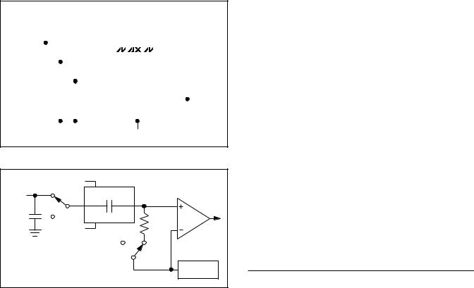
Figure 5. Equivalent Input Circuit
During the acquisition, the analog input (AIN) charges capacitor CDAC. The acquisition interval ends on the falling edge of the sixth clock cycle (Figure 6). At this instant, the T/H switches open. The retained charge on CDAC represents a sample of the input.
In hold mode, the capacitive digital-to-analog converter (DAC) adjusts during the remainder of the conversion cycle to restore node ZERO to zero within the limits of 14-bit resolution. At the end of the conversion, force CS high and then low to reset the input side of the CDAC switches back to AIN, and charge CDAC to the input signal again.
The time required for the T/H to acquire an input signal is a function of how quickly its input capacitance is charged. If the input signal’s source impedance is high, the acquisition time lengthens and more time must be allowed between conversions. The acquisition time (tACQ) is the maximum time the device takes to acquire the signal. Use the following formula to calculate acquisition time:
tACQ = 11(RS + RIN) x 35pF
where RIN = 800I, RS = the input signal’s source impedance, and tACQ is never less than 1.1Fs. A source impedance less than 1kI does not significantly affect the ADC’s performance.
To improve the input signal bandwidth under AC conditions, drive AIN with a wideband buffer (> 4MHz) that can drive the ADC’s input capacitance and settle quickly.
Input Bandwidth
The ADC’s input tracking circuitry has a 4MHz smallsignal bandwidth, so it is possible to digitize high-speed transient events and measure periodic signals with bandwidths exceeding the ADC’s sampling rate by using undersampling techniques. To avoid aliasing of unwanted high-frequency signals into the frequency band of interest, use anti-alias filtering.
Analog Input Protection
Internal protection diodes, which clamp the analog input to
AVDD and/or AGND, allow the input to swing from VAGND - 0.3V to VAVDD + 0.3V, without damaging the device.
If the analog input exceeds 300mV beyond the supplies, limit the input current to 10mA.
Digital Interface
Initialization After Power-Up and Starting a Conversion
The digital interface consists of two inputs, SCLK and CS, and one output, DOUT. A logic-high on CS places the MAX11101 in shutdown (autoshutdown) and places DOUT in a high-impedance state. A logic-low on CS places the MAX11101 in the fully powered mode.
To start a conversion, pull CS low. A falling edge on CS initiates an acquisition. SCLK drives the A/D conversion and shifts out the conversion results (MSB first) at DOUT.
Timing and Control
Conversion-start and data-read operations are controlled by the CS and SCLK digital inputs (Figure 6 and Figure 7). Ensure that the duty cycle on SCLK is between 40% and 60% at 4.8MHz (the maximum clock frequency). For lower clock frequencies, ensure that the minimum high and low times are at least 65ns. Conversions with SCLK rates less than 100kHz may result in reduced accuracy due to leakage.
Note: Coupling between SCLK and the analog inputs (AIN and REF) may result in an offset. Variations in frequency, duty cycle, or other aspects of the clock signal’s shape result in changing offset.


 Maxim Integrated Products 10
MAX11101
14-Bit, +5V, 200ksps ADC with 10µA Shutdown
CS |
|
|
|
|
|
|
|
|
|
|
|
|
|
|
|
|
|
|
|
SCLK |
1 |
4 |
6 |
8 |
|
|
12 |
|
|
|
16 |
|
|
|
20 |
|
|
|
24 |
|
tCSS |
tCH |
tCL |
|
|
|
|
|
|
|
|
|
|
|
|
|
|
|
tCSH |
|
|
|
|
|
|
|
|
|
|
|
|
|
|
|
|
|
|
||
DOUT |
|
|
D13 |
D12 |
D11 |
D10 |
D9 |
D8 |
D7 |
D6 |
D5 |
D4 |
D3 |
D2 |
D1 |
D0 |
S1 |
S0 |
|
|
|
|
|||||||||||||||||
tDN |
|
tACQ |
|
tDO |
|
|
|
|
|
|
|
|
|
|
|
|
|
|
tTR |
|
|
|
|
|
|
|
|
|
|
|
|
|
|
|
|
|
|
|
Figure 6. External Timing Diagram

 COMPLETE CONVERSION SEQUENCE
CS
DOUT
CONVERSION 0 |
|
CONVERSION 1 |
POWERED UP |
POWERED DOWN |
POWERED UP |
Figure 7. Shutdown Sequence
A CS falling edge initiates an acquisition sequence. The analog input is stored in the capacitive DAC, DOUT changes from high impedance to logic-low, and the ADC begins to convert after the sixth clock cycle. SCLK drives the conversion process and shifts out the conversion result on DOUT.
SCLK begins shifting out the data (MSB first) after the falling edge of the 8th SCLK pulse. Twenty-four falling clock edges are needed to shift out the eight leading zeros, 14 data bits, and 2 sub-bits (S1 and S0). Extra clock pulses occurring after the conversion result has been clocked
out, and prior to the rising edge of CS, produce trailing zeros at DOUT and have no effect on the converter operation.
Force CS high after reading the conversion’s LSB to reset the internal registers and place the MAX11101 in shutdown. For maximum throughput, force CS low again to initiate the next conversion immediately after the specified minimum time (tCSW).
Note: Forcing CS high in the middle of a conversion immediately aborts the conversion and places the MAX11101 in shutdown.


 Maxim Integrated Products 11