

MAX11101
14-Bit, +5V, 200ksps ADC with 10µA Shutdown
|
|
|
|
|
|
|
|
|
|
|
|
|
|
|
|
|
|
|
VDD |
|||||||
|
|
|
|
|
|
|
|
|
|
|
|
|
|
|
|
|
|
|
|
|
|
|
|
|
|
|
|
|
|
|
|
|
|
|
|
|
|
|
|
|
|
|
|
1mA |
|
|
|
|
|
||||
|
|
|
|
|
|
|
|
|
|
|
|
|
|
|
|
|
|
|
|
|
|
|||||
|
|
|
|
|
|
|
|
|
|
|
|
|
|
|
|
|
|
|||||||||
|
|
|
|
|
|
|
|
|
|
|
|
|
|
|
|
|
|
|
|
|
|
|
|
|
||
DOUT |
|
|
|
|
|
|
|
|
|
|
|
|
|
|
|
|
DOUT |
|
|
|
|
|
||||
1mA |
|
|
|
|
|
|
|
|
|
|
|
CLOAD = 50pF |
|
|
|
|
|
|
|
|
|
CLOAD = 50pF |
||||
|
|
|
|
|
|
|
|
|
|
|
|
|
|
|
|
|
|
|
|
|||||||
|
|
|
|
|
|
|
|
|
|
|
|
|
|
|
|
|
|
|
|
|||||||
|
|
|
|
|
|
|
|
DGND |
|
|
|
|
|
|
|
|
|
|
|
|
|
|
|
|
|
DGND |
|
|
|
|
|
|
|
|
|
|
|
|
|
|
|
|
|
|
|
|
|
|
|
||||
|
|
|
|
|
|
|
|
|
|
|
|
|
|
|
|
|
|
|
|
|||||||
|
|
|
|
|
|
|
|
|
|
|
|
|
|
|
|
|
||||||||||
|
|
|
|
|
|
|
a) VOL TO VOH |
b) HIGH-Z TO VOL AND VOH TO VOL |
||||||||||||||||||
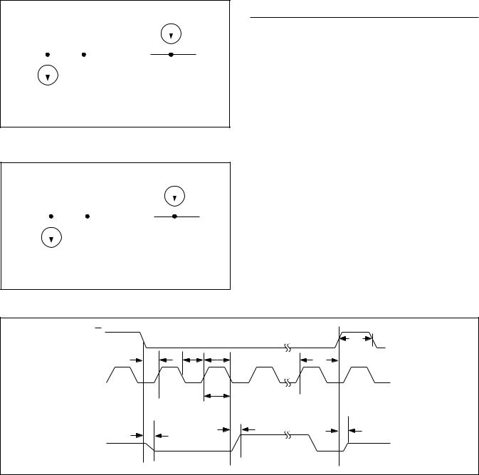
Figure 1. Load Circuits for DOUT Enable Time and SCLK to DOUT Delay Time
|
|
|
|
|
|
|
|
|
|
|
|
|
|
|
|
|
|
|
VDD |
|||||||
|
|
|
|
|
|
|
|
|
|
|
|
|
|
|
|
|
|
|
|
|
|
|
|
|
|
|
|
|
|
|
|
|
|
|
|
|
|
|
|
|
|
|
|
|
|
|
|
|
|
|
|
|
|
DOUT |
|
|
|
|
|
|
|
|
|
|
|
|
|
|
|
|
1mA |
|
|
|
|
|
||||
|
|
|
|
|
|
|
|
|
|
|
|
|
|
|
|
|
|
|
|
|
||||||
|
|
|
|
|
|
|
|
|
|
|
|
|
|
|
|
|
||||||||||
|
|
|
|
|
|
|
|
|
|
|
|
|
|
|
|
|
|
|
|
|
|
|
|
|||
|
|
|
|
|
|
|
|
|
|
|
|
|
|
|
|
DOUT |
|
|
|
|
|
|||||
1mA |
|
|
|
|
|
|
|
|
|
|
|
CLOAD = 50pF |
|
|
|
|
|
|
|
|
|
CLOAD = 50pF |
||||
|
|
|
|
|
|
|
|
|
|
|
|
|
|
|
|
|
|
|
|
|||||||
|
|
|
|
|
|
|
|
|
|
|
|
|
|
|
|
|
|
|
|
|||||||
|
|
|
|
|
|
|
|
DGND |
|
|
|
|
|
|
|
|
|
|
|
|
|
|
|
|
|
DGND |
|
|
|
|
|
|
|
|
|
|
|
|
|
|
|
|
|
|
|
|
|
|
|
||||
|
|
|
|
|
|
|
|
|
|
|
|
|
|
|
|
|
|
|
|
|||||||
|
|
|
|
|
|
|
|
|
|
|
|
|
|
|
|
|
||||||||||
|
|
|
|
|
|
a) VOH TO HIGH-Z |
b) VOL TO HIGH-Z |
|||||||||||||||||||
Figure 2. Load Circuits for DOUT Disable Time
Detailed Description
The MAX11101 includes an input track-and-hold (T/H) and successive-approximation register (SAR) circuitry to convert an analog input signal to a digital 14-bit output. Figure 4 shows the MAX11101 in its simplest configuration. The serial interface requires only three digital lines (SCLK, CS, and DOUT) and provides an easy interface to microprocessors (FPs).
The MAX11101 has two power modes: normal and shutdown. Driving CS high places the MAX11101 in shutdown, reducing the supply current to 0.1FA (typ), while pulling CS low places the MAX11101 in normal operating mode. Falling edges on CS initiate conversions that are driven by SCLK. The conversion result is available at DOUT in unipolar serial format. The serial data stream consists of eight zeros followed by the data bits (MSB first). Figure 3 shows the interface-timing diagram.
Analog Input
Figure 5 illustrates the input sampling architecture of the ADC. The voltage applied at REF sets the full-scale input voltage.
Track-and-Hold (T/H)
In track mode, the analog signal is acquired on the internal hold capacitor. In hold mode, the T/H switches open and the capacitive DAC samples the analog input.
CS
|
|
tCSW |
tCL |
tCH |
tCSH |
tCSS |
|
|
SCLK |
|
|
|
tCP |
|
tDV |
tDO |
tTR |
|
|
DOUT
Figure 3. Detailed Serial Interface Timing


 Maxim Integrated Products 9