

Understanding the Human Machine - A Primer for Bioengineering - Max E. Valentinuzzi
.pdf308 |
Understanding the Human Machine |
the cascade connection of two single units also linked by an overall feedback resistor RG . The latter supplies highly linear adjustable gain with-
out introducing common mode disturbances. Let us set up Kirchhoff’s node equations at both extremes of this resistor (which coincide with the negative input points, respectively, of each amplifier), say point I to A1 and point II to A2; that is,
(E2 − E1 ) RG +(Vo1 − E1 ) R3 = E1 R4 |
(5.15) |
(Vo − E2 ) R2 = (E2 −Vo1 ) R1 +(E2 − E)1 RG |
(5.16) |
The first equation (5.15) corresponds to point I and the second one (5.16) to point II. Take proper notice of the signs, as for example the first term in the first equation is positive because the difference of potential (E2 − E1 ) sustains a current towards the node. Besides, recall always that
potentials at the amplifiers inputs are equal so that E1 and E2 are used as
respectively equivalent to those of the negative terminals.
Let us briefly indicate the way to obtain the differential gain Gd of this circuit defined as Vo  (E2 − E1 ): First solve the first equation for Vo1 and, thereafter, solve the second equation also for Vo1 ; then, equate them and solve for Vo to get
Vo = E2 ×(R2 R1 + R2 |
RG + R2 R3 |
R1RG +1) |
(5.17) |
|
− E1 ×(R2 R1 + R2 RG + R2 R3 R1RG + R2 R3 R1R4 ) |
||||
|
||||
Comparison of equation (5.17) right-hand two terms quickly shows that both factors between parentheses would be exactly the same if the subterm R2 R3  R1R4 were forced to be 1, meaning that R2 R1 = R4 R3 = k ,
that is, when the resistors’ pairing or matching condition is met. In that case, the equation can be rewritten as
Vo = (E2 − E1 )×(R2 R1 + R2 |
RG + R2 R3 R1RG +1) |
(5.18) |
and the differential gain Gd |
appears as, |
|
Gd = (R2 R1 + R2 RG + R2 R3 |
R1RG +1) |
(5.19) |
Recalling the relationship k imposed above, the third term of this equation reduces to R4  RG and (5.19) becomes
1+ R2 R1 + R2 RG + R4 RG =1+ k +(R2 + R4 )/ RG . Finally, all four resistors

Chapter 5. Biological Amplifier |
309 |
can be made equal, i.e., R1 = R2 |
= R3 = R4 = R , and |
Gd = 2×(1+ R RG ) |
(5.20) |
showing that the differential gain of the amplifier based on two operational amplifiers depends only on the feedback resistor RG . The normal
operational amplifier circuit errors, resistor matching, and common mode swing characteristics limit the performance of this circuit. In this case, the common mode rejection errors of the two amplifiers tend to cancel each other out. Resistors must also be paired to optimize CMRR. Such condition is obtained, as before, by equating to zero the common mode gain. The relationship is as that given by equations (5.12). Modifying the gain with RG does not affect pairing and, as a consequence, does not af-
fect the CMRR either. Input impedance is high. All these added features make the circuit better than the previous one. A possible disadvantage is that the circuit is not symmetric, in other words, E1 is amplified by A1
and A2 while E2 is only amplified by A2 . Thus, both common mode
gains are different making impossible to reach zero level. However, the circuit can be implemented with inexpensive discrete components.
Based on equation (5.20), calculate the components needed to get a differential gain of 100. Remember that resistors higher than 200 or 250 kΩ are not recommendable. Repeat everything but for gains equal to 50 and to 200, respectively. Discuss.
5.3.3. Differential Amplifiers Based on Three Op-Amps
Figure 5.5 shows the most popular and already classic configuration of an instrumentation amplifier. The objective is to obtain the overall gain (which could also be called transfer function). Applying the principle of superposition, say for E1 = 0 , and the simple rules of the two basic ar-
rangements, that is, equation (5.1a) — the inverter — and equation (5.1b)
— the non-inverter — at the output of each amplifier, we get,
Va2 |
= E2 [(R1 + RG ) RG ] |
(5.21) |
Vb2 |
= −E2 (R1' RG ) |
(5.22) |
where the former corresponds to the non-inverter and the latter to the inverter.

310 |
Understanding the Human Machine |
Figure 5.5. DIFFERENTIAL AMPLIFIER BASED ON THREE OPERATIONAL AMPLIFIERS. Also commonly called instrumentation amplifier.
Similarly, with terminal E2 grounded, the partial voltages Va1 and Vb1 are given by,
Va1 |
= −E1 (R1' RG ) |
(5.23) |
Vb1 |
= E1[(R1' + RG ) RG ] |
(5.24) |
This time the first equation corresponds to the inverter and the second equation (5.24) to the non-inverter. From all four equations (5.21, 5.22, 5.23 and 5.24), the output voltages at points a and b are given as algebraic additions, or,
Va = E2 [(R1 + RG ) RG ]− E1 (R1' |
RG ) |
(5.25) |
Vb = E1[(R1' + RG ) RG ]− E2 (R1' |
RG ) |
(5.26) |
The final output voltage, Vo , after the third amplifier and applying the
superposition theorem, is obtained by grounding first point |
Vb and, |
thereafter, point Va . In mathematical terms, |
|
Vo = −(R3 R2 )×Va +[R3' (R2' + R3' )]×[(R3 + R2 ) R2 ]×Vb |
(5.27) |
We have already all the needed relationships. In order to manifest the differential action of the circuit, a better symmetry is brought about by making R3 = R3' , R2 = R2' and R1 = R1' , changing the latter equation into a simpler one, or,

Chapter 5. Biological Amplifier |
311 |
Vo = (Vb −Va )×(R3 R2 ) |
(5.28) |
which, after substituting for Va and Vb |
with equations (5.25) and (5.26) |
above, becomes |
|
Vo = (E1 − E2 )×[(2R1 RG )+1]×(R3 R2 ) |
(5.29) |
so establishing a clean-cut linear relationship between the output voltage and a differential input in a device made up with just three IC's and four resistors (without counting the power supply). The differential gain is only a matter of moving the differential input as divisor of Vo to the left.
This arrangement is divided in two stages: The first one (composed of two op-amps) provides high input impedance and some gain while the second stage (only one op-amp) improves the common mode rejection. Often, field effect transistors (FET) or bipolar input operational amplifiers are used for the first stage reaching values of Zin in the order of gigaohms (1 GΩ = 1012 Ω). Input-FET op-amps, however, generally have poorer CMRR than bipolar amplifiers. The second stage (or last op-amp) is decisive in the final determination of the CMRR. The curious student may find more details in the current literature or in the WEB or may wait until reaching the bioinstrumentation courses.
5.3.3.1. Common Mode Performance
The rationale is similar to that described above, that is, CMRR and gain, too, only depend on resistor's pairing ( R3 , R3' , R2 and R2' ). Besides, it can be demonstrated that CMRR is not influenced by R1 and R1' pairing.
Let us see,
The common mode output voltage Vocm is obtained applying at the input
a common mode signal Vincm = E1 = E2 , that is, by hooking together both terminals and connecting them to a source against the reference. Thus, equation (5.28) has to be used, giving,
Vocm = (Vacm −Vbcm )×(R3 |
R2 ) |
|
(5.30) |
where Vacm and –Vbcm |
should be replaced, respectively, by equations |
||
(5.25) and (5.26) yielding, |
|
|
|
Vacm =Vincm ×[(R1 + RG ) |
RG ]−Vincm ×(R1 |
RG ) |
(5.31) |
Vbcm =Vincm ×[(R1' + RG ) |
RG ]−Vincm ×(R1' |
RG ) |
(5.32) |
312 |
Understanding the Human Machine |
Considering that R1 = R1' , algebraic manipulation immediately shows a
null factor which makes Vocm = 0, so leading to the conclusion that the first stage resistors do not affect the CMRR. Hence, its gain, determined in part by RG, can be modified without increasing the common mode signal.
Resistors R1' , R1 and RG (Figure 5.5) can be complex impedances whose
effect in the frequency domain may be useful, as for example to reduce gain at the higher side of the spectrum. Possibilities are, in this respect, only limited by the designer's ingenuity. This first stage should have a relatively low gain, to avoid saturation from common mode inputs, whereas higher gain is reserved for the second stage, where saturation is not a problem. An instrumentation amplifier like this may reach voltage gains of 1,000 or higher with CMRR better than 80 dB, input impedance of a few GΩ and bias currents in the order of nA. In the last two decades or so, new and more efficient integrated circuit technologies have allowed significant reductions in production costs. There are devices in the market that include three op-amps. These are the basics of the subject that should permit the student to get around and even to solve some problems with.
Suggested exercise: Assuming the circuit shown in Figure 5.5, find the resistor values if the first stage has a gain equal to 5 and the second stage a gain equal to 10. Thereafter, consider a common mode input signal of 10 volts and calculate the undesired output signal with a CMRR of 66 dB and of 84 dB. Play a little with different numerical figures. Discuss.
5.4. Instrumentation Amplifier Specifications
An engineer makes measurements to know what kind of numbers he/she is dealing with, as for example to have an idea of the signals to handle or the environment the equipment is supposed to operate in (temperature, humidity, a vehicle, a highly noisy place) or any other special restriction (as space or weight). Based on these numbers and also on objectives clearly established, he/she sets a list of requirements, called specifications, the device is supposed to meet. Hence, the biological amplifier (perhaps to be placed in a surgery theater) and the instrumentation amplifier to implement it, always are accompanied by the specification sheet.

Chapter 5. Biological Amplifier |
313 |
In this section we will introduce and discuss the different data and their relative significance.
5.4.1. Basic Requirements
The manufacturer usually provides the data sheet or spec sheet (as sometimes is referred to in the daily jargon). It is obviously the end product core information; it concisely and numerically describes the unit to be installed in its working place. Even though the basic specifications cannot be improved, at least, some parameter compensation can be made. For example, the spec sheet may list, say,
Typical VS = ±15V |
Power supply |
RL = 2KΩ |
Load resistance |
TA = +25°C |
Ambient temperature |
Deviations from these conditions might degrade (or in some cases, improve, as for example with less stringent temperature requirements) the device's performance. The word “typical” often found in the spec sheet means that the datum was obtained in the factory during bench tests by averaging, in fact implying a probable different value around the stated one for the particular chip we bought. Other specifications have more precise definitions, or are based on several electronic determinations or knowledge and, thus, are beyond discussion.
5.4.2. Gain Range
The data sheet provides the gain equation to be applied for a given IC. It usually takes the form,
G =1+ 2×10⁵ R |
(5.33) |
G |
|
where RG [Ω] stands for the external resistor to be connected to a pair of stated pins. From it, for example, RG = 200,000 (G −1), yielding values
of G = 1 with RG = ∞ (open circuit) to G = 1001 for RG = 200 Ω. In practice, the external resistor is an R-network with at least a switch in order to choose a particular gain from a set of pre-established values. Resistors quality, wiring, contact resistances and stray capacitances will influence
314 |
Understanding the Human Machine |
the accuracy of the design and should be also considered. A single potentiometer is not a good solution.
Suggested exercise: Calculate a network to obtain, for a given IC (for example, an AD520; look it up in a manual), gain values of 10, 20, 50, 100, 200 and 500, including the switch connecting the resistor to the circuit terminals.
High gains (say, > 500) are in general not recommended because, when there is marked input noise or drift, they tend to worsen the situation. Eventually, if the information is to be digitized for further processing, gain can be compensated for in a subsequent stage (the so called gain trimming). Another piece of information refers to changes in gain due to changes in temperature. It is measured in parts per million per degree centigrade [ppm/°C]. Intelligent systems may correct for this error by means of a feedback loop.
Suggested experimental exercise: Test an IA (say, that mentioned before) by heating it up with a hair-drier and drawing the gain versus temperature curve.
5.4.3. Non-Linearity and Distortion
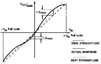
Non-linearity is the deviation from the expected straight line in a diagram plotting the output parameter versus the input parameter. When there is non-linearity, there is distortion of the reproduced waveform. Figure 5.6 depicts a transfer function (or gain) of a hypothetical device.
The horizontal axis represents the input voltage (say, in volts) and the vertical axis the output voltage (also in volts) but divided by the gain. This is an artifice to produce the ideal straight line at 45°, that is, bisecting the orthogonal system. When the horizontal axis is scanned from left to right measuring at each position the difference between the actual point on the curve and the theoretical point on the straight line, two maxima are found, ∆–max and ∆+max. The first one underestimates (“negative” deviation) while the second overestimates (“positive” deviation). The larger of the two in absolute terms divided by the corresponding input voltage (read below on the graph) is a measure of non-linearity and is expressed as “equal or smaller than the calculated percent”. Another way is by dividing that maximum deviation by the full-scale output range. Non-linearity can be corrected with a straight line fitting procedure in which the slope and offset voltage are modified until |∆+max| = |∆–max|.
Chapter 5. Biological Amplifier |
315 |
Figure 5.6. TRANSFER FUNCTION ILLUSTRATING NON-LINEARITY.
Figure 5.6 shows such line (dotted). Such criterion is the base of the sometimes-called Best Straight Line Method.
5.4.4. Input Characteristics
They can be described in terms of voltage, current and impedance and, as such, should be separately treated although, in fact, they are inter-related. Input Voltage Range refers to the maximum applicable value. For example, the type AD524 accepts up to ±10 Volts. Many times, this parameter is given both for differential and common mode inputs.
Input Current is zero in the ideal op-amp, but this is real life and, no matter how much we may dislike it, it is small and finite; at least two types are to be accounted for:
1) Input Bias Current is sustained by the power supply, which keeps the active elements alive in any circuit. Devices with FET at the input have very low bias current but they are strongly dependent on temperature. Thus, it is important to determine their sensitivity to it. Typical values, say for an AD620A range between 0.5 to 2.0 nA. Often, only the maximum value is supplied.
2) Input Offset Current is defined as the difference between the two bias currents (one per terminal); hence, it is a residual current, some kind of left-over of an imperfect circuit. In spite of the differential input, the bias
316 |
Understanding the Human Machine |
current requires a return pathway to the reference terminal. Otherwise, amplifier saturation and drift could reach unacceptable levels.
In both types of current (bias and offset), their sensitivity to temperature changes is given in pA or nA per degree centigrade.
Input Impedance (Differential and Common Mode), appears as critical if one recalls the loading effect it has on the desired biological signal to be recorded. Once more, it is a fact of the biomedical engineer's life making us gently smile of the preached ideal infinity. For the IA depicted in Figure 5.5, the first stage two op-amps input impedances, in turn dependent on the factory technology, define the overall input impedance. It may reach from a few MΩ to a few GΩ. The IC AD524, as an example, has a specified value of 109 Ω, in the differential and in the common mode as well.
5.4.5. Common Mode Rejection Ratio
The higher this parameter, the better the behavior of the device. Usually, it is specified for full range input voltage at a given source imbalance. Since it depends on the gain, the latter is also given (Bronzino, 1995). We suggest to experimentally test an IA so that the student can have a hands-on feeling. Review the definitions and equations given above and remember the two input terminals must be hooked together to inject a common mode signal.
5.4.6. Voltage Offset and Drift
Above, we introduce the offset current. We should not be surprise if there is also an offset voltage. If a direct current (dc) amplifier output — with its input terminals short-circuited and grounded — is connected to a paper recorder running at very slow speed during several hours, a line moving slowly up and down will be obtained; that is, the recording pen did not stay at the same level, it drifted aimlessly. Moreover, as soon as the output is connected to the recorder, the output voltage (which should be zero for a zero input) shows a well measurable offset.
Offsets are due to intrinsic imbalance of the input circuits (FET's or other) and are also dependent on the temperature. Drift is a consequence of instabilities and is also dependent on temperature.
The total offset at the output has two components; the input-offset voltage multiplied by the amplifier's gain and the output-offset voltage inde-
Chapter 5. Biological Amplifier |
317 |
pendent on the gain. For higher gains, there is a dominance of the former, while for lower gains the latter tends to have more weight. The technologies behind the IC’s implementing the amplifiers have decidedly a strong influence on the actual values. Drift is quantitatively expressed in terms of rate, as volts per day or per month and also as volts per day per degree centigrade.
Offset voltage can be compensated for in some types with an internal adjustment via an ad-hoc external potentiometer. However, it may not be a full solution because the bias condition is usually modified and/or there is thermal interaction with the device. The commonest way is by means of an external voltage applied to the reference terminal. The data sheet itself usually hints this kind of arrangement. Finally, the offset voltage is many times referred to the voltage supply, so attempting to quantify fluctuations effects of the latter on the former.
5.4.7. Frequency Response
The dynamic range of the amplifier depends on the frequency band it can handle. Biological signals have low amplitude and extend from 0 Hz (dc) up to a few hundred Hz in most of the cases, or even up to 10 kHz when the electromyogram is recorded or in high fidelity electrocardiography. In comparison with amplifiers in other fields, the biological amplifier requires a reduced bandwidth and is always shifted to the low side.
The data sheet often provides the gain versus frequency plot or it gives the high cut-off frequency, that is, the frequency at which gain drops 3 dB. For a few ac biological amplifiers, as in electrocardiography, the low cut-off is also given (in the order of fraction of Hz). Typical values for IA's are well above the requirements of any physiological signal.
There are two time related parameters, which conceptually belong to the category of dynamic characteristics: Settling Time and Recovery Time. The first one is defined as the total time required for the output to respond to a fast full-scale input step. It is some kind of lag time or “iner- tia-like” phenomenon found in many other systems. Typical values are in the order of 10 to 75 µs (rather fast, indeed) and it does not necessarily show gain dependency.
Transient discharges (as from cardiac pacemakers, defibrillators, electrosugery equipments) may get into the biological amplifier, imposing an overload, and driving it into saturation. How long does it take to recover,