

Много теории
.pdf4.2. Improved Fully Etched Grating Coupler
where ne denotes the e ective index of the TE mode in the grating region.
|
0 |
|
|
|
|
|
|
|
−5 |
|
|
|
|
|
|
|
−10 |
|
|
|
|
|
|
(dB) |
−15 |
|
|
|
|
|
|
power |
|
|
|
|
|
|
|
|
|
|
|
|
|
|
|
|
−20 |
|
|
|
|
|
|
|
|
|
|
|
Directionality |
|
|
|
−25 |
|
|
|
InsertionLoss−New |
|
|
|
|
|
|
ReflectionToWG |
|
||
|
|
|
|
|
InsertionLoss−old |
|
|
|
−30 |
|
|
|
ReflectionToWG−old |
||
|
1450 |
1500 |
1550 |
1600 |
1650 |
1700 |
|
|
1400 |
||||||
|
|
|
wavelength (nm) |
|
|
||
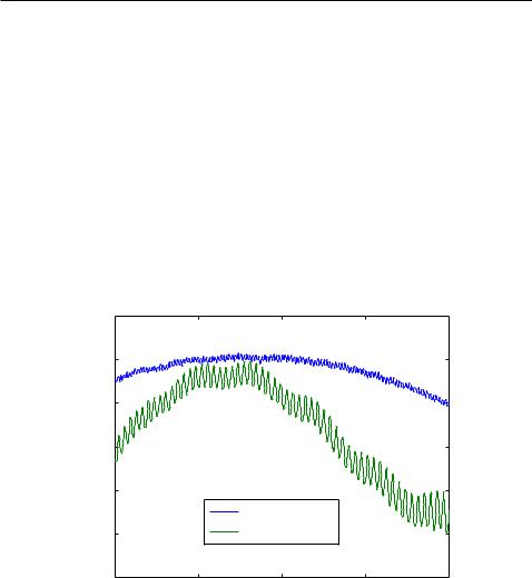
Figure 4.9: Comparison of regular fully etched grating coupler and the fully etched grating coupler with minor sub-wavelength gratings.
4.2.2Simulation Results
FDTD method has been used to simulate and optimize the grating structure. The simulations were based on the SOI wafer we used for fabrication, with a 2 um buried oxide and 220 nm top Si layer. Silicon oxide was employed as the cladding for protection. Particle Swarm Optimization (PSO), which is an optimization algorithm for electromagnetic optimization problems [39, 61], has been used to optimize the grating design. Design parameters, i.e., grating period, duty cycle, and the width of the minor gratings were optimized to achieve small back re ection as well as low insertion loss. The optimized design has a period of 625 nm, a duty cycle of 190nm, and sub-wavelength gratings with a width of 50 nm.
Figure 4.9 shows the simulation results of a regular fully etched grating coupler and the fully etched grating coupler with minor sub-wavelength
67
4.2. Improved Fully Etched Grating Coupler
gratings. The dash lines denote the insertion loss and the back re ection of the regular fully etched grating coupler, and the solid lines denote the directionality, insertion loss, and the back re ection of the proposed grating coupler. More than 64% (-1.9 dB) of the input power from the waveguide was di racted upwards by the grating. However, due to the mode mismatch between the grating coupler and the bre, only 45% (-3.47 dB) of light from the waveguide was coupled in the fundamental mode of bre. The back re ection of the grating coupler is reduced from -6 dB to about -18 dB, which is similar to that of a shallow etched grating coupler.
4.2.3Measurement Results
|
−10 |
|
|
|
|
|
−15 |
|
|
|
|
(dB) |
−20 |
|
|
|
|
−25 |
|
|
|
|
|
power |
|
|
|
|
|
−30 |
|
|
|
|
|
|
|
|
|
|
|
|
|
|
SubGC |
|
|
|
−35 |
|
General FGC |
|
|
|
−40 |
1540 |
1560 |
1580 |
1600 |
|
1520 |
||||
|
|
|
wavelength (nm) |
|
|
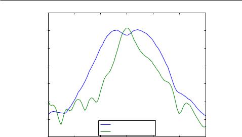
Figure 4.10: Measurement results of the regular fully etched grating coupler and the fully-etched grating coupler with minor sub-wavelength gratings
Test structures, consisting of an input coupler and an output coupler, of the fully etched grating couplers with minor sub-wavelength gratings have been fabricated through electron beam lithography at University of Washington using the JEOL JBX-6300FS E-Beam Lithography system. Test
68

4.2. Improved Fully Etched Grating Coupler
structures of regular fully etched grating couplers have also been fabricated for the comparison purpose. Measurement spectra of the regular fully etched grating coupler and the fully etched grating coupler with minor subwavelength gratings are shown in Fig. 4.10. Green curve donates the results of the regular fully etched grating coupler and the blue curve denotes the proposed fully etched grating coupler with minor sub-wavelength gratings. The extinction ratio of the ripples have been reduced from about 3dB to about 0.8 dB, by implementing the minor sub-wavelength gratings. The insertion loss of the grating coupler is also improved by about 2 dB. In addition, the bandwidth of the proposed design is largely improved, which is nearly twice as that of the regular fully etched grating coupler.
69
Chapter 5
Vertical Grating Coupler
All of the grating couplers mentioned so far are detuned grating couplers, which indicates the case that a small angle is employed between the incident wave to the normal of the grating surface. The small angle is introduced to avoid the second order Bragg re ection [15], but such a small angle is not desirable for a low-cost packaging process [5]. In this chapter, grating couplers for perfectly vertical coupling will be presented, and a bidirectional grating coupler for vertical coupling will be demonstrated to improve the insertion loss of the vertical grating couplers.
5.1Regular Vertical Grating Couplers
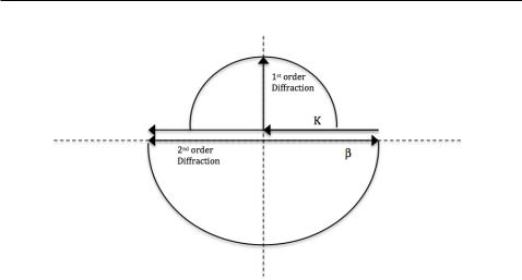
The main drawback of the vertical grating coupler is the large second order re ection to the waveguide, which can be predicted by the Bragg condition:
sin = m K |
(5.1) |
where denotes the wave vector of the propagated mode within the grating,
denotes the di raction angle, m is an integer denoting the di raction order, and K = = . In the case where the rst order di raction is perfectly coupled to the bre, i.e., = 0 when m = 1, = K, i.e., = =ne, where ne denotes the e ective index of the grating and denotes the central wavelength. In this case, the second order di raction of the grating is in the direction of the input waveguide, i.e., = 90 when m = 2. The wave vector diagram of a vertical grating coupler is shown in Fig. 5.1.
70
5.1. Regular Vertical Grating Couplers
Figure 5.1: Diagram of wave vectors for vertical grating coupler
A vertical grating coupler is designed based on a SOI wafer with a 2 um buried oxide and a 220 nm top Si layer. A shallow etch layer with an etch depth of 70 nm is used and SiO2 is employed as the cladding for protection. The designed central wavelength is 1550 nm and FDTD simulations have been used to nd the optimized design with low insertion loss and large bandwidth around the desired wavelength. The e ective index of the 220 nm Si layer is 2.83 (ne 1), and the e ective index of the shallow etched
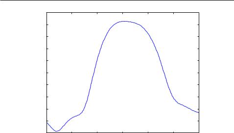
Si layer is 2.506 (ne 2). Therefore, the e ective index of the grating can be calculated by ne = ne 1=2 + ne 2=2, which is 2.668. Grating period of the desired grating can be calculated from the Bragg condition with the known e ective index of the grating, which is 580 nanometers in our case. Further optimization of design parameters such as grating period and duty cycle have been done using FDTD methods. Figure 5.2 shows simulation results of the insertion loss and back re ection to waveguide of an optimized regular vertical grating coupler. The blue curve denotes the insertion loss and the green curve denotes the back re ection to the waveguide. A valley is shown in the spectrum of the insertion loss, which is caused by the large back re ection.
71
5.1. Regular Vertical Grating Couplers
|
0 |
|
|
|
|
|
|
|
−5 |
|
|
|
|
|
|
|
−10 |
|
|
|
|
|
|
(dB) |
−15 |
|
|
|
|
|
|
|
|
|
|
|
|
|
|
power |
−20 |
|
|
|
|
|
|
|
|
|
|
|
|
|
|
|
−25 |
|
|
|
|
|
|
|
−30 |
|
|
Insertion loss |
|
|
|
|
|
|
|
|
|
|
|
|
−35 |
|
|
Reflection to WG |
|
|
|
|
1450 |
1500 |
1550 |
1600 |
1650 |
1700 |
|
|
1400 |
||||||
|
|
|
wavelength (nm) |
|
|
||
Figure 5.2: Insertion loss and back re ection of a regular vertical grating coupler
Di erent approaches have been employed to avoid the large second order re ection of the vertical grating couplers [4, 5, 40, 57]. Asymmetric grating structure [40] has been used to avoid the large Bragg re ection for vertical coupling. However, the extra etch depth required for fabrication increases the complexity as well as the cost. Chirped gratings were also implemented to minimize the mode mismatch between the grating and optical bre [4, 5]. However, high fabrication accuracy is required to fabricate those chirped grating couplers. Given the fabrication accuracy of the existing technology, the stability and repeatability of the chirped gratings are still doubted. Another drawback of the chided grating coupler is their small bandwidth. The reported 3dB bandwidth of the chirped vertical grating coupler is only about 45 nanometers. Slanted grating coupler was proposed to obtain high coupling e ciency to a vertically positioned optical bre [57]. However, the technology required for fabrication of the slanted grating slit is too compacted to be compatible with standard CMOS technology, and therefore only suitable for prototyping.
72
5.2.Bidirectional Grating Coupler
5.2Bidirectional Grating Coupler
5.2.1Device Layout
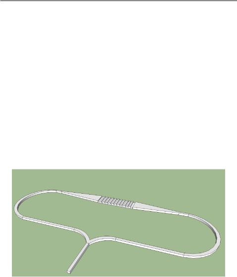
The regular vertical grating couplers only couple light from one side of the grating. Theoretically, the insertion loss of such vertical grating couplers with uniform gratings can exceed 50 %. Here we introduced a bidirectional grating coupler structure for vertical grating, which breaks the theoretical limitation of regular vertical grating couplers. A schematic of the bidirectional grating coupler is shown in Fig. 5.2. Basically, it is a symmetric structure with the grating in the centre. Two-dimensional tapers are connected to both sides of the grating to convert the mode into the waveguides. Bending waveguides are employed to direct the light from both sides of the grating into a 50-50 coupler. Finally, light from both sides of the grating is combined together with a 50-50 coupler.
Figure 5.3: Schematic of bidirectional grating coupler for vertical coupling
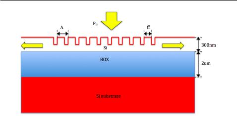
Figure 5.4 shows the cross-section of the bidirectional vertical grating coupler designed in a SOI wafter with a 2 um buried oxide and a 300 nm top Si layer. A shallow etch layer (ed = 155nm) has been employed by the design, and SiO2 is used as the cladding for protection. denotes the grating period and ff denotes the duty cycle of the grating coupler.
73
5.2. Bidirectional Grating Coupler
Figure 5.4: Cross section of a bidirectional grating coupler
5.2.2Design and Simulation
FDTD method has been used to design and simulate the bidirectional grating coupler design. The grating period of the grating coupler can be predicted by the Bragg condition. Given that the e ective index of the 300 nm slab waveguide is 3.052 (ne 1), and the e ective index of the 145 nm slab waveguide is 2.571 (ne 2), the e ective index of the grating (ne ) can be obtained, i.e., ne = 0:5 ne 1 + 0:5 ne 2, which is 2.812 in our case. The desired central wavelength is 1550 nanometers, so the grating period can be obtained from the Bragg condition, which is about 550 nm in our case.
2D FDTD simulations were used to further optimize the design. Three parameters, i.e., the number of grating, grating period, and the duty cycle were optimized using the Particle Swarm Optimization algorithm to achieve a design with low insertion loss and large bandwidth. The number of grating period determines the length of the coupling region. As the length of the grating region increases, the directionality of the grating increases, which means more power can be di racted to the bre, but extra scattering loss will be introduced as the light propagates from the grating to the waveguide. On the other hand, shorter grating region can reduce the scattering loss, but the directionality of the grating will decrease. The grating period along with
74
5.2. Bidirectional Grating Coupler
|
0 |
|
|
|
|
|
|
|
−2 |
|
|
|
|
|
|
|
−4 |
|
|
|
|
|
|
|
−6 |
|
|
|
|
|
|
(db) |
−8 |
|
|
|
|
|
|
|
|
|
|
|
|
|
|
power |
−10 |
|
|
|
|
|
|
−12 |
|
|
|
|
|
|
|
|
|
|
|
|
|
|
|
|
−14 |
|
|
|
|
|
|
|
−16 |
|
|
|
|
|
|
|
−18 |
|
|
|
|
|
|
|
−20 |
1450 |
1500 |
1550 |
1600 |
1650 |
1700 |
|
1400 |
||||||
|
|
|
wavelength (nm) |
|
|
||
Figure 5.5: The insertion loss of the optimized bidirectional grating coupler
the duty cycle of the grating determines the central wavelength of the grating coupler. The optimized design has a grating number of 13, a grating period of 580 nanometers, and a duty cycle of 240 nanometers. The insertion loss of the optimized bidirectional vertical grating couple is shown in Fig. 5.5. The insertion loss is calculated with the assumption that the taper and Y junction are lossless. The assumption holds because theoretically a tape with a length of 200 micron can achieve lossless conversion from 12 um grating to a 500 nm wire waveguide[50], and compact Y junction with low loss has been demonstrated [42, 61]. The insertion loss of the optimized grating coupler is only -1.5 dB, which is much smaller than of that of the regular vertical grating coupler. The 3dB bandwidth of the bidirectional grating coupler is more than 100 nanometers, which is more than twice of the value reported in [5].
The optical waves in di erent sides of the grating behave like two arms of a MZI. The insertion loss shown in Fig. 5.5 can be only obtained when the incident wave from the bre impinges in the middle of the grating coupler. In the case when the incident wave is o from the centre of the grating, optical
75
5.2. Bidirectional Grating Coupler
|
0 |
|
|
|
|
|
|
|
−5 |
|
|
|
|
|
|
|
−10 |
|
|
|
|
|
|
(dB) |
−15 |
|
|
|
|
|
|
|
|
|
|
|
|
|
|
power |
−20 |
|
|
|
|
|
|
|
|
|
dx=0 |
|
|
|
|
|
|
|
|
|
|
|
|
|
−25 |
|
|
dx=40nm |
|
|
|
|
|
|
dx=80nm |
|
|
||
|
|
|
|
|
|
||
|
−30 |
|
|
dx=120nm |
|
|
|
|
|
|
dx=160nm |
|
|
||
|
|
|
|
|
|
||
|
−35 |
1450 |
1500 |
1550 |
1600 |
1650 |
1700 |
|
1400 |
||||||
|
|
|
wavelength (nm) |
|
|
||
Figure 5.6: Insertion of the bidirectional vertical grating coupler as function of wavelength for di erent o set
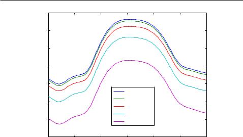
waves from the two arms interfere with each other at the junction of the 50-50 coupler. Depending on the deviation of the incident wave, either constructive interference or destructive interference can be obtained at the 50-50 coupler. Figure 5.6 shows the simulation results of the bidirectional grating coupler with various deviation values. The deviation of the input wave, i.e., dx shown in Fig. 5.7, is de ned as the distance from centre of the input bre core to the centre of the grating. The e ective index of the channel waveguide used in our case is about 2.4, and the central wavelength of the input wave is 1550nm. According to the phase condition between the propagated wave in the two arm, i.e., ne 2dx = =2, the rst destructive interference will obtained be when dx = 160nm. Fig. 5.6 shows the simulation results for various deviation values. As the deviation, dx, goes beyond 160 nm, the insertion loss of the vertical grating coupler will be somewhere in between the maximum value and the minimum value. From the simulation results shown in Fig. 5.6, we note that the insertion loss of the bidirectional vertical grating coupler is very sensitive to the position of the input bre, which results in
76