

Много теории
.pdf1.5.Polarization of Waveguide Modes
1.5Polarization of Waveguide Modes
If we orient our coordinate system so that the interface between the silicon and the cladding and the interface between the silicon and the buried oxide lie in the xz plane (shown in Fig. 1.3) and the guided mode propagates along the z axis, then the wave vectors for the incident, re ected, and transmitted waves are all contained in the yz plane. Thus the yz plane is called the plane of incidence [19]. Transverse electric (TE) modes are de ned as these modes having their electric elds perpendicular to the plane of incidence (i.e. x axis here) and transverse magnetic (TM) modes are de ned as these modes having their magnetic elds perpendicular to the plane of incidence. The amplitude of the electric eld and magnetic eld of the fundamental ( rst order or lowest order) TE-like mode are shown in Fig. 1.4. The amplitude of the electric eld and magnetic eld of the fundamental TM-like mode are shown in Fig. 1.5. By comparing the amplitude of the fundamental TE-like mode and the fundamental TM-like mode, we can see that the TE-like mode is better con ned than the TM-like mode. In all subsequent sections of this thesis, channel waveguides are assumed, and we will drop the -like extension and refer to the modes as simple TE and TM modes.
The propagation constant, , is employed to represent the behaviour of di erent modes within the channel waveguide and is de ned as [19]:
= |
2 |
|
n |
e |
(1.1) |
|
0 |
||||||
|
|
|
where 0 denotes the operation wavelength and ne denotes the e ective refractive index of the mode. The e ective refractive index is introduced to describe and compare the con ned modes within the channel waveguide and is de ned as:
ne = |
c |
= |
|
(1.2) |
|
|
|||
vp |
k0 |
where c is the speed of light in vacuum, vp is the phase velocity of the mode, and k0 denotes the wave vector in free space, i.e., k0 = 2 = .
7

1.6.State-of-the-art Grating Couplers
1.6State-of-the-art Grating Couplers
Some state-of-the-art grating couplers are listed in Table 1.1. Important parameters such as central wavelength, polarization, insertion loss, and bandwidth, for comparison purpose, are shown in the table. Corresponding fabrication details are also listed because the performance of a grating coupler is highly dependent on how it is made. The insertion loss of the grating coupler is mainly determined by the thickness of the top silicon layer and the thickness of the buried oxide (BOX), because these two values a ect the phase conditions of di erent wavelengths at the interface between the grating layer and the buried oxide layer. Bottom distributed Bragg re ectors (DBR) [31] and top overlays [56] have been used to decrease the insertion loss, but nonstandard wafers and fabrication processes are required for these approaches. Both shallow etched and fully etched grating couplers are shown in the table and the central wavelengths are around 1550 nm and 1310 nm, which are in the two most commonly used optical windows in telecommunications. These grating couplers listed are mainly designed for TE mode operation.
8
1.6. State-of-the-art Grating Couplers
micron
0.4
0.3
0.2
0.1
0
−0.1
−0.2
−0.3
−0.4 |
0 |
0.5 |
−0.5 |
micron
(a)
0.8
0.7
0.6
0.5
0.4
0.3
0.2
0.1
micron
0.4
0.3
0.2
0.1
0
−0.1
−0.2
−0.3
−0.4 |
0 |
0.5 |
−0.5 |
micron
(b)
x 10−5 7
6
5
4
3
2
1
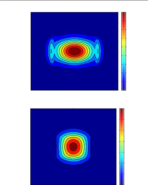
Figure 1.4: (a) The amplitude of the electric eld of the rst order TE-like mode in a rectangular channel waveguide; (b) The amplitude of the magneticeld of the rst order TE-like mode in a rectangular channel waveguide [9]
9
1.6. State-of-the-art Grating Couplers
micron
0.4
0.3
0.2
0.1
0
−0.1
−0.2
−0.3
−0.4 |
0 |
0.5 |
−0.5 |
micron
(a)
0.8
0.7
0.6
0.5
0.4
0.3
0.2
0.1
micron
0.4
0.3
0.2
0.1
0
−0.1
−0.2
−0.3
−0.4 |
0 |
0.5 |
−0.5 |
micron
(b)
x 10−5 4.5
4
3.5
3
2.5
2
1.5
1
0.5
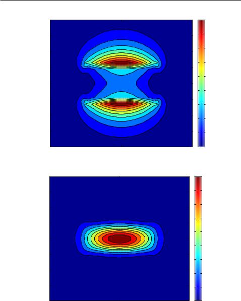
Figure 1.5: (a)The amplitude of the electric eld of the rst order TM-like mode in a rectangular channel waveguide; (b)The amplitude of the magneticled of the rst order TM-like mode in a rectangular channel waveguide [9]
10

|
|
Wavelength |
Polarization |
Insertion Loss |
Bandwidth |
Process |
|
|
|
|
|
|
|
2006 |
[48] |
1550nm |
TE |
-5.1 dB |
40nm (1dB) |
220nm Si, 1um BOX, shallow etch |
|
|
|
|
|
|
|
2010 |
[56] |
1530nm |
TE |
-1.6dB |
80nm (3dB) |
amorphous Si overlay, shallow etch |
|
|
|
|
|
|
|
2010 |
[3] |
1530nm |
TE |
-1.2dB |
N/A |
340nm Si, 2um BOX, shallow etch |
|
|
|
|
|
|
|
2011 |
[35] |
1310nm |
TE |
-3dB |
58nm |
400nm Si, shallow etch |
2012 |
[60] |
1550nm |
TE |
-4.4dB |
45nm (1.5dB) |
220nm Si, 2um BOX, shallow etch |
|
|
|
|
|
|
|
2012 |
[31] |
1490nm |
TE |
-0.75 dB |
N/A |
shallow etch, bottom DBR |
|
|
|
|
|
|
|
2010 |
[13] |
1550nm |
TM |
-3.7dB |
60nm |
full etch |
|
|
|
|
|
|
|
2012 |
[58] |
1550nm |
TE |
-2.29dB |
60nm |
full etch, 250 Si ,1um BOX |
|
|
|
|
|
|
|
Table 1.1: State-of-the-art grating couplers
11
Couplers Grating art-the-of-State .6.1
1.7. Measurement Setup
1.7Measurement Setup
(a)
(b)
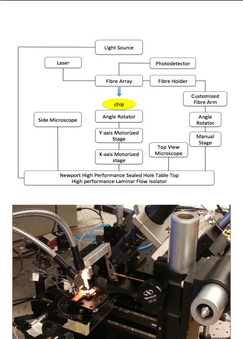
Figure 1.6: (a) Illustration of the automated setup; (b) automated setup
12
1.7. Measurement Setup
The automated setup used for the measurement of the devices shown in this thesis are built by Charlie Lin [26] and Jonas Flueckiger. The illustration and physical map of the automated setup are shown in Fig. 1.6 (a) and Fig. 1.6(b), respectively. The chip is placed on a platform which is on top of an angle rotator. An X-axis motorized stage and a Y-axis stage are seated below the angle rotator, which forms a cross con guration. Thebre array ribbon is held by a custom-made aluminum bre ribbon holder, which is suspended on top of the chip platform. An aluminum arm is used to hold the bre ribbon holder and is attached to an angle rotator (shown in Fig. 1.7). The angle rotator is xed onto a Z-axis actuator that is bolted to a raised platform so the bre ribbon height can be manually adjusted accordingly. The ribbon-to-chip image is captured two microscopes; one microscope shows the top view and is used for alignment purpose; the other microscope is angled from the side to display the height displacement between the bre array and the chip to prevent crashing the bre array into the chip during alignment. The light source for the microscopes illuminates the chip platform at an angle from behind the bre ribbon [26].
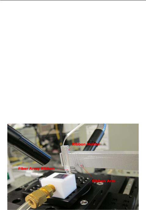
Figure 1.7: Fibre array ribbon, ribbon holder and ribbon arm [26]
13
Chapter 2
Theory And Numerical
Methods
In this chapter, we will give a short overview on the fundamental theories and numerical methods related to grating coupler design. We will start from Bragg's Law, from which we will derive the most fundamental theory to deal with periodic structures, i.e., the Bragg condition. Also, the e ective Index Method (EIM) will be introduced to obtain an approximation of the e ective index of refraction of a slab waveguide. Finally, the Finite-Di erence Time Domain (FDTD) method is introduced to obtain the optimized solution for the grating coupler design and to predict the performance.
2.1Bragg Condition
2.1.1Bragg's Law
A schematic of Bragg's Law is shown in Fig. 2.1. Periodic dots are seated in the air with a period of d in the y direction. A plane wave is incident on the periodic structure and is scattered by each plane periodic dots in such a way that the portion scattered from the second plane of dots undergoes an extra length of 2dsin( ), as compared to the portion scattered by the rst plane of dots. Depending on the phase condition, either constructive interference or destructive interference occurs. Constructive interference occurs when the extra length is equal to an integer multiple of the wavelength of the incident wave, i.e.:
2 d sin = m |
(2.1) |
14

2.1. Bragg Condition
where m is an integer, is the wavelength of the incident wave, and is the scattering angle.
Figure 2.1: Bragg's Law
2.1.2The Bragg Condition for Grating Coupler
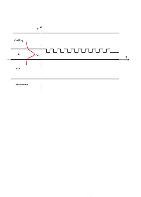
The most fundamental formula concerning periodic structures is Bragg condition. The grating coupler discussed in this thesis is a one-dimensional periodic structure, as shown in Fig. 2.2. In Fig. 2.2 we assume that the wave incident on the grating is a guided wave propagating in a slab waveguide, and its direction of propagation is in the same plane as the grating and is normal to the grating teeth. The general form of the Bragg condition can be expressed as:
kz = m K |
(2.2) |
where denotes the wave vector of the input wave, i.e., = 2 nwg= , nwg denotes the e ective index of the incident wave, kz denotes the component of the wave vector of the di racted wave in the direction of the incident wave, where kz = 2 nc= ; and K = 2 = , which is determined by the periodicity
15
2.1. Bragg Condition
of the structure. This relation can also be depicted by a diagram shown in Fig. 2.3, which is easier to understand.
Figure 2.2: Schematic of a grating coupler
The di ractions of a grating coupler can be observed in those directions where constructive interference is achieved. Each value of m that results in di raction is referred to as the m-th order di raction:
ne nc sin = m |
(2.3) |
where ne denotes the e ective index of the grating, nc denotes the e ective index of the bre mode in the cladding, denotes the period of the grating,
denotes the di raction angle, denotes the wavelength of the incident wave (or out-coupled wave), and m is an integer denoting the di raction order. The di raction order normally used for coupling is the rst order (i.e., m = 1), so the Bragg Condition for a grating coupler can be further simpli ed to:
ne nc sin( ) = |
|
(2.4) |
|
It should be noted that the Bragg condition is only exact for in nite gratings, i.e., one-dimensional grating with in nite grating period. In a
16