

Много теории
.pdf3.1. Detuned Shallow Etched Grating Coupler
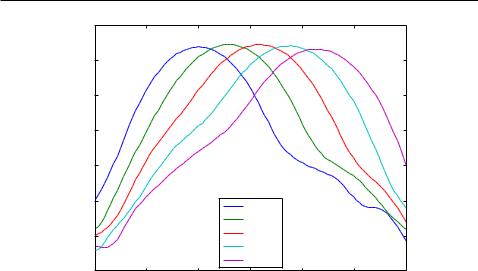
calculated to be 660 nanometers. The insertion loss and back re ection of the initial grating coupler are shown in Fig. 3.1. The central wavelength of the initial grating coupler design is 1553nm, with an insertion loss of -3.1dB and a 3dB bandwidth of 70nm.
|
0 |
|
|
|
|
|
|
|
−5 |
|
|
|
|
|
|
|
−10 |
|
|
|
|
|
|
(dB) |
−15 |
|
|
InsertionLoss |
|
|
|
|
|
|
|
|
|||
power |
|
|
|
|
|
||
−20 |
|
|
Reflection |
|
|
|
|
|
|
|
|
|
|
||
|
|
|
|
|
|
|
|
|
−25 |
|
|
|
|
|
|
|
−30 |
|
|
|
|
|
|
|
−35 |
1450 |
1500 |
1550 |
1600 |
1650 |
1700 |
|
1400 |
||||||
|
|
|
wavelength (nm) |
|
|
||
Figure 3.1: Insertion loss and back re ection to the waveguide of the initial grating coupler
3.1.2Design Parameters
Once we got the initial condition, optimization of the design can be achieved by sweeping di erent design parameters such as the grating period, the duty cycle, the etch depth, and the incident angle. The impacts that each of the parameters has on the grating coupler are described in the following sections.
Grating Period
Grating period in uences the performance of a grating coupler through the following equation:
= |
|
(3.3) |
ne nc sin( ) |
27
3.1. Detuned Shallow Etched Grating Coupler
|
0 |
|
|
|
|
|
|
|
−5 |
|
|
|
|
|
|
|
−10 |
|
|
|
|
|
|
(dB) |
−15 |
|
|
|
|
|
|
|
|
|
|
|
|
|
|
power |
−20 |
|
|
|
|
|
|
|
|
|
|
|
|
|
|
|
−25 |
|
|
620nm |
|
|
|
|
|
|
|
|
|
|
|
|
|
|
|
640nm |
|
|
|
|
−30 |
|
|
660nm |
|
|
|
|
|
|
|
680nm |
|
|
|
|
−35 |
|
|
700nm |
|
|
|
|
1450 |
1500 |
1550 |
1600 |
1650 |
1700 |
|
|
1400 |
||||||
|
|
|
wavelength (nm) |
|
|
||
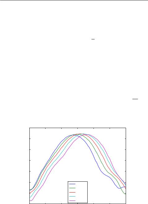
Figure 3.2: Variations of grating period
where denotes the period of the grating coupler, denotes the central wavelength, ne denotes the e ective index of the grating, nc denotes the e ective refractive index of the bre mode and denotes the incident angle. As shown in the equation, the central wavelength of the grating coupler is proportional to the grating period. Figure. 3.2 shows the simulation results for varying the grating period. We kept nc = 1, = 20 , and ff = 0:5. As we varied the grating period from 620 nanometers to 700 nanometers, the central wavelength of the grating coupler shifted from 1500 nanometers to 1612 nanometers. The redshift shown in the central wavelength is consistent with our analytical calculation. And the tuning coe cient of the grating period, which is de ned as = , was calculated to be 1.4 nm=nm.
28
3.1. Detuned Shallow Etched Grating Coupler
Duty Cycle
Duty cycle a ects the performance of a grating coupler through its impact on the e ective index of refraction of the grating:
ne = nc sin( ) + |
|
(3.4) |
|
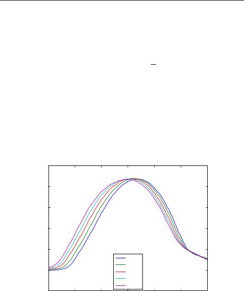
where ne denotes the e ective index of refraction of the grating, is the incident angle and is the central wavelength. For a given grating period, the e ective index of refraction of the grating is proportional to the duty cycle of the grating. Figure. 3.3 shows the simulation results for varying duty cycle. We kept grating period constant at 660 nanometers and varied the duty cycle from 230 nanometers to 430 nanometers. The central wavelength shifted from 1536 nanometers to 1579 nanometers as we varied the duty cycle. The tuning coe cient of the duty cycle, which is de ned as W , was calculated to be 0.215 nm=nm. By comparing Fig. 3.3 and Fig. 3.2, we note that grating period has a stronger impact on the central wavelength of the grating than the duty cycle does.
|
0 |
|
|
|
|
|
|
|
−5 |
|
|
|
|
|
|
|
−10 |
|
|
|
|
|
|
(dB) |
−15 |
|
|
|
|
|
|
|
|
|
|
|
|
|
|
power |
−20 |
|
|
|
|
|
|
|
|
|
|
|
|
|
|
|
−25 |
|
|
230nm |
|
|
|
|
|
|
|
|
|
|
|
|
|
|
|
280nm |
|
|
|
|
−30 |
|
|
330nm |
|
|
|
|
|
|
|
380nm |
|
|
|
|
−35 |
|
|
430nm |
|
|
|
|
1450 |
1500 |
1550 |
1600 |
1650 |
1700 |
|
|
1400 |
||||||
|
|
|
wavelength (nm) |
|
|
||
Figure 3.3: Variations of duty cycle
29
3.1. Detuned Shallow Etched Grating Coupler
Etch Depth
Etch depth of a grating coupler also in uences the performance of the grating coupler through its impact on the e ective index of refraction of the grating:
ne = nc sin( ) + |
|
(3.5) |
|
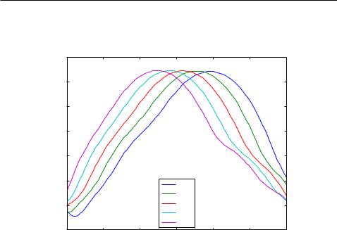
where ne denotes the e ective index of refraction of the grating, denotes the incident angle, and denotes the central wavelength. As the etch depth increases, the e ective index of refraction of the shallow etched area decreases, thus ne decreases. The e ective index of refraction is proportional to the central wavelength of the grating, so the etch depth of the grating coupler is inversely proportional to the central wavelength of the grating. Figure. 3.4 shows the simulation results for varying the etch depth. We
|
0 |
|
|
|
|
|
|
|
−5 |
|
|
|
|
|
|
|
−10 |
|
|
|
|
|
|
(dB) |
−15 |
|
|
|
|
|
|
power |
|
|
|
|
|
|
|
|
|
|
|
|
|
|
|
|
−20 |
|
|
|
|
|
|
|
|
|
|
60nm |
|
|
|
|
−25 |
|
|
65nm |
|
|
|
|
|
|
70nm |
|
|
|
|
|
|
|
|
75nm |
|
|
|
|
−30 |
|
|
80nm |
|
|
|
|
1450 |
1500 |
1550 |
1600 |
1650 |
1700 |
|
|
1400 |
||||||
|
|
|
wavelength (nm) |
|
|
||
Figure 3.4: Variations of etch depth
kept grating period, duty cycle, incident angle constant and varied the etch depth of the grating coupler from 60 nanometers to 80 nanometers. The central wavelength shows a blueshift as the etch depth increases, which is
30
3.1. Detuned Shallow Etched Grating Coupler
consistent with our analytical calculation. The tuning coe cient of the etch depth, which is de nes as = ed, was calculated to be 1.9 nm=nm.
|
0 |
|
|
|
|
|
|
|
−5 |
|
|
|
|
|
|
|
−10 |
|
|
|
|
|
|
(dB) |
−15 |
|
|
|
|
|
|
|
|
|
|
|
|
|
|
power |
−20 |
|
|
|
|
|
|
|
|
|
|
|
|
|
|
|
−25 |
|
|
15 |
|
|
|
|
|
|
|
|
|
|
|
|
|
|
|
17.5 |
|
|
|
|
−30 |
|
|
20 |
|
|
|
|
|
|
|
22.5 |
|
|
|
|
−35 |
|
|
25 |
|
|
|
|
1450 |
1500 |
1550 |
1600 |
1650 |
1700 |
|
|
1400 |
||||||
|
|
|
wavelength (nm) |
|
|
||
Figure 3.5: Variations of incident angle
Incident Angle
The incident angle of a grating coupler is de ned as the angle between the incident wave (or out-coupled wave) and the normal to the grating surface. A positive angle indicates the case in which the incident wave and the coupled wave in the waveguide propagate in the same direction and a negative angle indicates the case in which the incident wave and the coupled wave in the waveguide propagate in opposite directions. The incident angle in uences the central wavelength of the grating coupler through the following equation:
sin( ) = |
ne |
(3.6) |
|
nc |
|||
|
|
where ne denotes the e ective index of refraction of the grating, is the central wavelength, is the grating period and nc denotes the e ective index
31
3.1. Detuned Shallow Etched Grating Coupler
of the wave incident on the grating. Simulation results for varying incident angle are shown in Figure 3.5. We kept the grating period, duty cycle and etch depth of the grating constant. As we increased the incident angle from 15 degree to 25 degree, the central wavelength shifted from 1594 nanometers to1524 nanometers. So the tuning coe cient, which de ned as = , was calculated to be 7 nm=degree.
From the simulation results shown above, we can see that grating period, duty cycle, etch depth and incident angle all have impacts on the central wavelength of the grating coupler, but the tuning coe cient is different. Table 3.2 shows the comparison of the tuning coe cients of various parameters.
Parameter |
period |
duty cycle |
etch depth |
incident angle |
|
|
|
|
|
|
|
|
|
|
Tuning coe cient |
1.4 nm=nm |
0.215 nm=nm |
1.9 nm=nm |
7 nm=degree |
|
|
|
|
|
Table 3.2: Tuning coe cients of various parameters
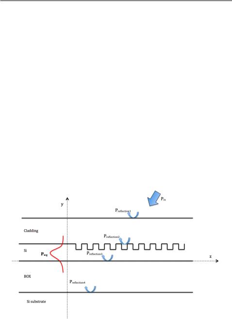
Figure 3.6: Schematic of re ections at di erent interfaces
32
3.1. Detuned Shallow Etched Grating Coupler
Cladding and Buried Oxide
The thickness of the buried oxide and the thickness of the cladding are two important factors that have impacts on the insertion loss of the grating coupler. An illustration of di erent re ections at various interfaces of the grating coupler is shown in Figure. 3.6. The phase conditions between those re ections determine the insertion loss of the grating coupler. Minimum insertion loss can be achieved when Pre ection1 and Pre ection2 result in destructive interference and Pre ection3 and Pre ection4 result in destructive interference.
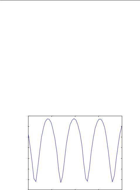
Simulation results for varying buried oxide are shown in Figure. 3.7. As we varied the thickness of the buried oxide from 1 um to 3 um, the insertion loss of the grating coupler changed in a sinusoidal way, which is determined by the phase condition between Pre ection1 and Pre ection2. The thickness of the buried oxide for a particular wafer type is chosen to achieve constructive interference between Pre ection1 and Pre ection2, therefore, low insertion loss can be obtained.
|
−3 |
|
−4 |
|
−5 |
(dB) |
−6 |
|
|
power |
−7 |
|
|
|
−8 |
|
−9 |
|
−10 |
1 |
1.5 |
2 |
2.5 |
3 |
|
|
thickness of the BOX (um) |
|
|
Figure 3.7: Variations for BOX thickness
33
3.1. Detuned Shallow Etched Grating Coupler
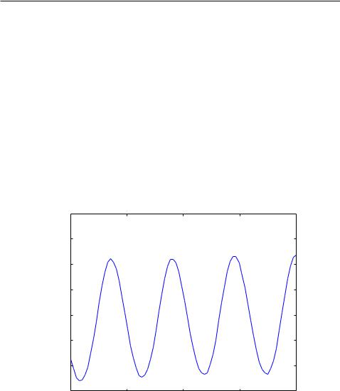
Similarly, the phase condition of Pre ection3 and Pre ection4 varies as the thickness of the cladding changes. We de ne the thickness of the cladding to be the height from the interface of the silicon and buried oxide to the top surface of the cladding. Figure. 3.8 shows the simulation results for varying the cladding thickness. Minimum insertion loss achieved where destructive interference occurs and maximum insertion loss achieved where constructive interference occurs. Depending on the incident angle and the central wavelength, the optimal thickness of cladding changes. By comparing Fig. 3.7 and Fig. 3.8 we note that the thickness of the buried oxide has a larger impact on the insertion loss of the grating. This is the case because the re ection coe cients of Pre ection3 and Pre ection4 are larger than those of
Pre ection1 and Pre ection2.
|
−2 |
|
−2.2 |
|
−2.4 |
(dB) |
−2.6 |
|
|
power |
−2.8 |
|
|
|
−3 |
|
−3.2 |
|
−3.4 |
1 |
1.5 |
2 |
2.5 |
3 |
|
thickness of the cladding (um) |
|
||
Figure 3.8: Variations for cladding thickness
3.1.3Optimization of the Grating Coupler
Optimization of a grating coupler involves simulation sweeps of various parameters such as grating period, duty cycle, and incident angle, etc, but
34
3.1. Detuned Shallow Etched Grating Coupler
not all of parameters are variable. The thickness of di erent layers are determined by the wafer type, whereas the etch depth and the cladding are normally determined by the fabrication process. So the design variables are the grating period, duty cycle, and incident angle. The optimization process requires a lot of simulation sweeps on those design variables. Figure. 3.9 shows the simulation and measurement results of the grating coupler designed for the fabrication process provided by Opsis-IME [1]. The designed grating coupler has a grating period of 650 nanometers with a duty cycle of 350 nanometers. The simulated results show an insertion loss of -2.74dB with a 3dB bandwidth of 79.8nm, and the measurement shows an insertion loss of -4.64dB with a 3dB bandwidth of 74.9nm. The simulation results shown in Fig. 3.9 is obtained from the model shown in Fig. 2.9 (a) with the assumption that the distance between the bre tip and the chip is negligible.
|
−2 |
|
|
|
|
|
|
−4 |
|
|
|
|
|
(dB) |
−6 |
|
|
|
|
|
|
|
|
|
|
|
|
power |
−8 |
|
|
|
|
|
|
|
Simulation |
|
|
||
|
|
|
|
|
||
|
−10 |
|
Measurement |
|
|
|
|
|
|
|
|
|
|
|
−12 |
1520 |
1540 |
1560 |
1580 |
1600 |
|
1500 |
|||||
|
|
|
wavelength (nm) |
|
|
|
Figure 3.9: Grating coupler design fabricated through OpSIS-IME
From Fig. 3.9 we note that the measured insertion loss is smaller than the simulated insertion loss. In addition, the bandwidth of the measured spectrum is narrower than that of the simulated one. The mismatches in insertion loss and bandwidth mainly results from the gap between the bre
35
3.1. Detuned Shallow Etched Grating Coupler
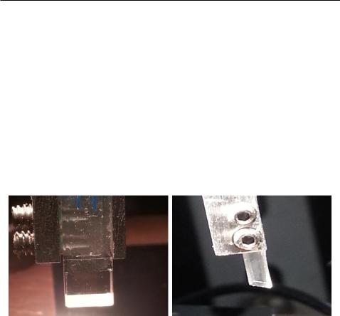
ribbon and the photonics chip. The images of the bre ribbon used in our measurement setup are shown in Fig. 3.10. The tip of the bre ribbon is polished at 20.3 degrees. According to Snell's Law, if the bre tip is parallel to the photonics chip, it will give us a 30 degree incident angle in the air. In order to get a 20 degree incident angle in air, we need to rotate the bre ribbon (as shown in the right image of Fig. 3.10). In this case, there will be a gap between the tip of the bre ribbon and the photonic chip. In addition, extra space is left intentionally to protect the chip from scratching by the ribbon. So a large air gap exists between the ribbon and the photonic chip. The mode pro le becomes larger as it propagates between the bre ribbon and the chip, which introduces extra loss and narrows the bandwidth.
Figure 3.10: Images of bre ribbon
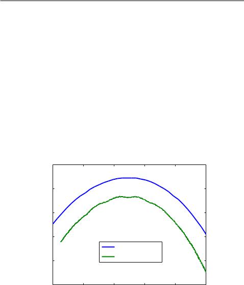
Figure. 3.11 shows the impact of the gap between the bre ribbon and the measured photonic chip. The blue curve indicates the change in insertion loss and the green curve indicates the change in bandwidth. For each value of the gap, i.e., the distance from the bre to the chip, we optimized the XY position of the bre to achieve lowest insertional loss. As we varied the gap from 0 to 200 nanometers, the insertion loss of the grating coupler decrease from -2.47dB to -6.08 dB and the bandwidth decreased from 77 nanometers to 44.5 nanometers.
36