

Много теории
.pdf2.2. E ective Index Method
Figure 2.3: Diagram for Bragg condition
nite grating, there is not a discrete k-vector for which di raction occurs, but a range of k-vectors around the one predicted by the Bragg condition [49].
2.2E ective Index Method
The E ective Index Method (EIM) was initially proposed for the analysis of dielectric waveguides with rectangular cores [24]. The basic idea of this method is to replace a two-dimensional waveguide with a one-dimensional one with an e ective index derived from the geometry and refractive index of the original structure [7]. The EIM has been applied to various structures such as optical waveguides [17, 29], optical bres [7], and waveguide arrays [8].
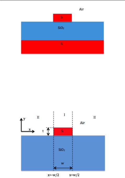
Figure 2.4 shows the schematic of a silicon-on-insulator waveguide. It is a three-layer structure with SiO2 (n=1.444) in the middle and Si (n=3.47) layers on the top and bottom. Air (n=1) has been employed as the cladding in this structure. The procedure for calculating the e ective index for silicon-
17
2.2. E ective Index Method
Figure 2.4: Cross section of silicon-on-insulator waveguide
on-insulator waveguide with a two-dimensional cross-section is shown in Fig. 2.5 and Fig. 2.6. The basic approach is to solve the mode condition for a particular mode type in one dimension and nd the propagation constant. The e ective index can be derived from the propagation constant, ne = =k0, and then applied to the other dimension of the structure [19].
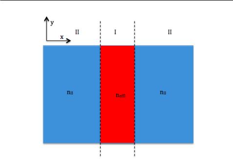
Figure 2.5: Schematic of a SOI strip waveguide
18
2.2. E ective Index Method
Figure 2.6: Schematic of the e ective index of a strip waveguide
To begin with, we divide the structure into three regions. These three regions are x < w=2, w=2 < x < w=2, and w=2 < x, where w denote the width of the silicon waveguide. The cladding of the waveguide is air, which has a refractive index of 1. Next we decide on the mode type that we wish to solve for. For the lowest order TE-like mode, the T E0 mode, we solve the mode condition for TE modes in the y-direction of a slab waveguide with the refractive index pro le in region I. The mode condition for TE modes within region I can be expressed by [19]:
ht = m + tan 1( |
q |
) + tan 1 |
( |
p |
); m = 0; 1; 2; ::: |
(2.5) |
||||||
|
|
|||||||||||
|
h |
|
h |
|
||||||||
h = q |
|
|
|
|
|
|||||||
k02n22 2 |
(2.6) |
|||||||||||
p = q |
|
|
|
|
||||||||
2 k02n32 |
(2.7) |
|||||||||||
q = q |
|
|
|
|||||||||
2 k02n12 |
(2.8) |
|||||||||||
19

2.2. E ective Index Method
where m is the mode order, n1, n2 , n3 , are the refractive index of the cladding, silicon core and SiO2, respectively. is the propagation constant of the mode supported by the slab waveguide, which is de ned as k0ne I, where ne I is the e ective index of the mode within the slab waveguide in region I.
Now we create the one-dimensional waveguide structure shown in Fig. 2.6, in which our calculated ne I is used for the central slab, i.e., for region I. The refractive index chosen for region II depends on the actual structure; nevertheless, for SOI strip waveguides with air cladding, one can use refractive index of the air, i.e., n=1. In the x-direction, the mode condition is solved for the appropriate TM mode of the structure. The condition for TM modes can be expressed as [19]:
ht = m + tan 1( |
q |
) + tan 1 |
( |
p |
); m = 0; 1; 2; ::: |
(2.9) |
||
|
|
|||||||
|
h |
|
|
|
h |
|
||
|
|
|
n2 |
|
|
|
|
|
|
p = |
2 |
p |
|
|
|
(2.10) |
|
|
n2 |
|
|
|
||||
|
|
|
3 |
|
|
|
|
|
|
|
|
n2 |
|
|
|
|
|
|
q = |
2 |
q |
|
|
|
(2.11) |
|
|
n2 |
|
|
|
||||
|
|
|
1 |
|
|
|
|
|
Using the EIM, we have now successfully converted a two-dimensional waveguide into a one-dimensional structure, and then solved for that structure. By doing this, the EIM enables us to simulate three-dimensional structures as two-dimensional ones, which saves signi cant computational e ort and time. Following on this idea, we can take complex three-dimensional waveguides and reduce them to two-dimensional systems in which each waveguide is replaced by its e ective index in a plane that is parallel to the the interface of the Si layer and the BOX layer.
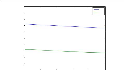
The e ective index of refraction of a strip waveguide, with a dimension of 220 nm by 500 nm, for both T E0 and T M0 modes, as a function of wavelength, are shown in Fig. 2.7. The T E0 mode has a larger e ective index than the T M0 mode because the TE mode is better con ned within the waveguide. In this thesis, we only use the rst step of the EIM to nd the e ective index of the slab waveguide which forms the grating coupler.
20
2.3. Finite-Di erence Time-Domain Method
effective index
3 |
|
|
|
|
TE |
|
|
|
|
|
|
2.8 |
|
|
|
|
TM |
2.6 |
|
|
|
|
|
2.4 |
|
|
|
|
|
2.2 |
|
|
|
|
|
2 |
|
|
|
|
|
1.8 |
|
|
|
|
|
1.6 |
|
|
|
|
|
1.4 |
|
|
|
|
|
1.2 |
|
|
|
|
|
1 |
1520 |
1540 |
1560 |
1580 |
1600 |
1500 |
wavelength (nm)
Figure 2.7: E ective index of TE and TM modes
2.3Finite-Di erence Time-Domain Method
The components used in photonic integrated circuits are normally complicated three-dimensional structures such as gratings, rings, waveguide couplers, etc. It is not possible to obtain the exact analytical solutions for these structures, except for some special cases. In practice, we use numerical methods to obtain the solutions for such structures. Finite-Di erential Time-Domain (FDTD) method is a very popular numerical method used for obtaining solutions to two-dimensional and three-dimensional structures.
When Maxwell's di erential equations are examined, it can be seen that the change in the E- eld in time (the time derivative) depends on the change in the H- eld in space (the curl). This results in the basic FDTD timestepping relation that, at any point in space, the updated value of the E- eld in time depends on the stored value of the E- eld and the numerical curl of the local distribution of the H- eld in space[59]. The H- eld is time-stepped in a similar manner. At any point in space, the updated value of the H- eld in time is dependent on the stored value of the H- eld and the numerical
21
2.3. Finite-Di erence Time-Domain Method
curl of the local distribution of the E- eld in space. Iterating the E- eld and H- eld updates results in a \marching-in-time" process, wherein sampleddata analogs of the continuous electromagnetic waves under consideration propagate in a numerical grid stored in the computer memory[18].
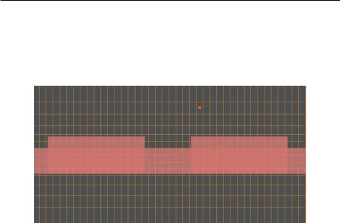
Figure 2.8: FDTD mesh for a grating coupler
During the simulation, the structure is discretized using a uniform grid as shown in Fig. 2.8. A brute-force calculation of Maxwell's equations on each mesh point will be operated within the time domain. The simulation accuracy is highly dependent on the grid size. A smaller grid size is required to get more accurate results. The advantage of the FDTD method is that it can deal with arbitrarily complicated structures. However, the drawback of this method is long calculation times and large computational memory is required for accurate simulations. The FDTD method may not be appropriate for simulating extra long structures, but it is ideal for simulating compact structures such as grating couplers. FDTD Solutions, a commercial product from Lumerical Solutions Inc., was employed as the simulation tool for all grating couplers in this thesis.
22

2.3. Finite-Di erence Time-Domain Method
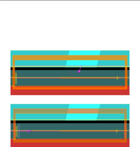
Two-dimensional simulations are generally used to simulate grating couplers because it takes much less computational memory and simulation time. After designing a grating using 2D simulations, 3D simulations are used to verify the behaviours of the nal design. The schematic shown in Fig. 2.9 depicts a general grating coupler structure: a Si layer on the bottom for mechanical strength, a functional Si layer on top of 2-um buried oxide, and a top oxide layer for protection. The orange rectangle de nes the simulation region and Perfectly Matched Layer (PML) boundary is used so that radiation appears to propagate out of the computational area and therefore, does not interfere with the elds inside. The yellow lines shown in the graphs represent frequency-domain power monitors which collect highaccuracy power ow information in the frequency domain from simulation results across spatial regions within the simulation. The green area denotes the bre, the purpose of which will be explained below.
Two types of simulation structures are often employed to simulate a grating coupler. Figure. 2.9 (a) is used to simulate the input grating coupler and Fig. 2.9 (b) is used to simulate the output grating coupler. A polished optical bre is presented on top of the cladding, with a light green area indicating the bre core and a dark green area indicating the cladding of the bre. For an input grating coupler, a fundamental TE mode is launched from the bre core and coupled into the waveguide by the grating. Power monitors are used to record the insertion loss and re ection to the bre of the grating coupler. For an output grating coupler, a fundamental TE mode is launched from the waveguide and out-coupled into the bre. A mode expansion monitor is used to calculate the power that goes into the fundamental mode of the bre [18]. This is essential for a coupler because not all of the power is coupled into the fundamental mode due to the mode mismatch.
23
2.3. Finite-Di erence Time-Domain Method
(a)
(b)
Figure 2.9: (a) Schematic of simulation structure for input grating coupler;
(b) Schematic of simulation structure for output grating coupler
24
Chapter 3
Detuned Grating Coupler
The most important properties for a grating coupler are the insertion loss, the back re ection to the waveguide, and the bandwidth. Compared to the fully etched grating couplers, shallow etched grating couplers have the advantages of high coupling e ciency and low back re ection to the waveguide. So it is more popularly employed in the integrated photonics circuits. A small angle is often employed between the incident wave and the normal of the grating surface, so that the large second order Bragg re ection can be avoided, which is called the detuned case.
In this chapter, the design ow for detuned shallow etched grating couplers will be presented, and the in uences of various factors on the properties of the grating couplers will be discussed in detail. In addition, a universal grating coupler design methodology will be introduced to generate shallow etched grating couplers, using analytic calculations instead of numeric simulations.
3.1Detuned Shallow Etched Grating Coupler
Designing a grating coupler follows a procedure. The rst step is to get the initial condition of the desired grating coupler using theoretical calculations, and the second step is to optimize the performance of the initial design by sweeping various parameters such as grating period, duty cycle, and incident angle.
25

3.1.Detuned Shallow Etched Grating Coupler
3.1.1Initial Condition
Designing a grating coupler should follow some restrictions: some of the parameters are determined by the wafer type we use, such as the thickness of the silicon layer and the thickness of the buried oxide; some of the parameters are determined by the fabrication process, such as the cladding material, the etch depth, and the minimum feature size; and some of the parameters are decided by the application and tunability of the measurement setup, such as the central wavelength and the incident angle. In our case, all the known initial values are listed in Table 3.1.
Si |
SiO2 |
Cladding |
Etch Depth |
|
|
|
|
|
|
|
|
220 nm |
2um |
air |
70 nm |
1550 nm |
20 degree |
Table 3.1: Initial values
Given the initial values listed in Table 3.1, we can calculate the e ective index of refraction of the grating. We used the Finite-di erence time-domain (FDTD) method to calculate the e ective index of refraction of the grating. The e ective index of refraction of the shallow etched slab waveguide, ne 1, is calculated to be 2.534, and the e ective index of refraction of the unetched slab waveguide, ne 2, is calculated to be 2.848. Thus, the overall e ective index of refraction of the grating ne can be calculated from the following equation:
ne = ne 1 ff + ne 2 (1 ff) |
(3.1) |
where ff denotes the ll factor of the grating coupler. With the e ective index of refraction of the grating, we can get the grating period, , from the Bragg condition:
nc sin = ne |
|
(3.2) |
|
where nc denotes the e ective index of the bre mode, denotes the incident angle, ne denotes the e ective index of refraction of the grating, and denotes the desired central wavelength. In our case, the grating period was
26