

Много теории
.pdf3.1. Detuned Shallow Etched Grating Coupler
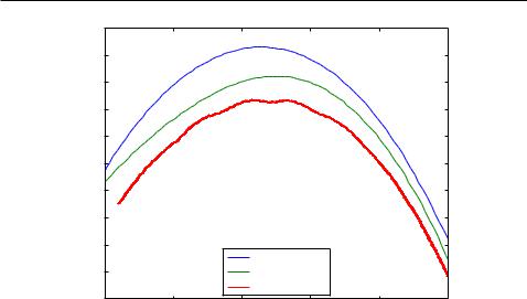
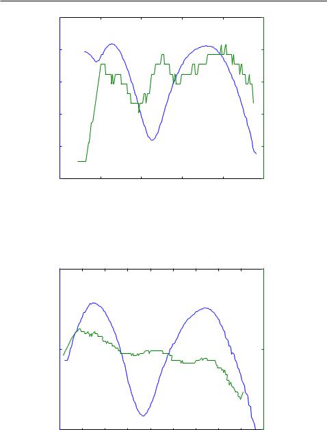
According to the simulation results shown in Fig. 3.11, we revised our simulation model and simulated the grating coupler design shown in Fig. 3.9 with a 25 um air gap between the bre ribbon tip and the chip. The comparison of the simulation results and measurement results of the grating coupler are shown in Fig. 3.12. The blue curve denotes the simulation results of the grating structure with 1um air gap between the bre ribbon tip and the chip, the green curve denotes the simulation results with a 25 um air gap between the grating and the chip, and the red curve denotes the measurement results for the same gating design. As we take the air gap between thebre ribbon tip and the grating into consideration, a closer match between the simulation results and the measurement results have been achieved. The remaining mismatch of insertion loss mainly comes from the optical connections of the measurement system, such as the connections between the bre and the laser and the connection between the bre and the detector.
0 |
|
|
|
80 |
|
−5 |
|
|
|
60 |
Bandwidth (nm) |
Insertion Loss(dB) |
|
|
|
|
|
−10 |
50 |
100 |
150 |
40 |
|
0 |
200 |
|
|||
|
Gap between fiber ribbon and chip (um) |
|
|
||
Figure 3.11: Impacts of the gap between bre ribbon tip and photonic chip on the insertion loss and bandwidth of the grating coupler
37
3.1. Detuned Shallow Etched Grating Coupler
|
−2 |
|
|
|
|
|
|
−3 |
|
|
|
|
|
|
−4 |
|
|
|
|
|
|
−5 |
|
|
|
|
|
(dB) |
−6 |
|
|
|
|
|
−7 |
|
|
|
|
|
|
power |
|
|
|
|
|
|
−8 |
|
|
|
|
|
|
|
|
|
|
|
|
|
|
−9 |
|
|
|
|
|
|
−10 |
|
Gap=1um |
|
|
|
|
|
|
|
|
||
|
−11 |
|
Gap=25um |
|
|
|
|
−12 |
|
Measurement |
|
|
|
|
1520 |
1540 |
1560 |
1580 |
1600 |
|
|
1500 |
|||||
|
|
|
wavelength (nm) |
|
|
|
Figure 3.12: Spectra of simulation results with di erent gap distance and measurement results
3.1.4Design Stability
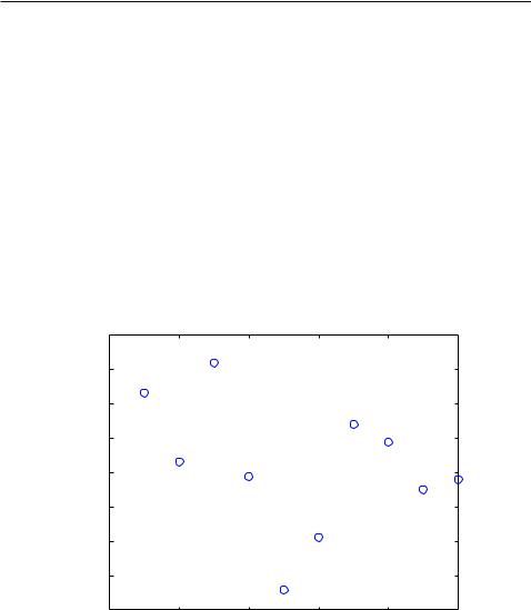
To examine the stability of the grating coupler design at di erent positions on the same photonic chip, we measured the performance of the same grating coupler design at di erent positions of the chip. The fabrication of the grating couplers were done by electron beam lithography at University of Washington. The grating coupler is designed based on a wafer with 2um buried oxide and 220 nm top Si layer. A shallow etch layer with an etch depth of 70 nm was used and air was employed as the cladding. The insertion losses, 3dB bandwidths, and the central wavelengths of the same design at 10 di erent positions were measured and the comparison of these results are shown in Fig. 3.13, Fig. 3.14, and Fig. 3.15. Fig. 3.13 shows the insertion losses of the same grating coupler design at di erent positions of the chip. The measured insertion losses are between -7.58dB and -8.24 dB. In order to protect the chip from scratching, we intentional left a gap between the chip the bre tip. Therefore, the insertion loss of the measurement results is
38
3.1. Detuned Shallow Etched Grating Coupler
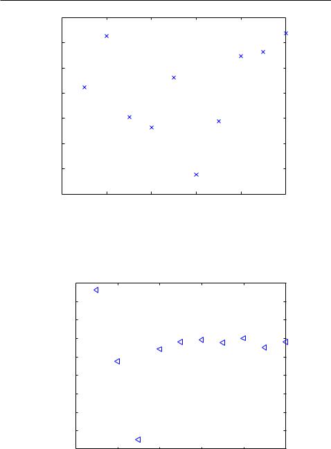
much larger than the simulation results. However, the stability in insertion loss of the grating coupler has been observed. Fig. 3.14 shows the measurement results of 3dB bandwidths of the same grating coupler at 10 di erent positions. The measured 3dB bandwidths of the grating coupler is between 47.5 nm and 42 nm. The chip may not perfectly aligned horizontally, which results in di erent gap distances between the bre ribbon tip and the chip at di erent positions. The variations in gap distances is the main source for di erences in bandwidth. Fig. 3.15 shows the central wavelengths of the same grating coupler design at di erent positions of the chip. Most of the measured grating couplers have a central wavelength of about 1550 nm, which is the designed central wavelength. The small discrepancy in central wavelength indicates the high accuracy of the fabrication process.
Insertion loss (dB)
−7.5
−7.6
−7.7
−7.8
−7.9
−8
−8.1
−8.2
−8.3
0 |
2 |
4 |
6 |
8 |
10 |
Device ID
Figure 3.13: The insertion losses of the same grating coupler design at different positions of the chip
39
3.1. Detuned Shallow Etched Grating Coupler
3dB bandwidth (nm)
48
47
46
45
44
43
42
41 |
2 |
4 |
6 |
8 |
10 |
0 |
Device ID
Figure 3.14: The 3dB bandwidths of the same grating coupler design at di erent positions of the chip
central wavelength (nm)
1551.5
1551
1550.5
1550
1549.5
1549
1548.5
1548
1547.5
1547 |
2 |
4 |
6 |
8 |
10 |
0 |
Device ID
Figure 3.15: The central wavelengths of the same grating coupler design at di erent positions of the chip
40

3.2.Universal Grating Coupler Design
3.2Universal Grating Coupler Design
Depending on the fabrication process and applications, various grating couplers are required [16, 32, 35, 44, 56]. The traditional way of designing grating couplers involves brute-force simulations on all of the design parameters, which is very time-consuming and a lot of computational memory is required. Here we present a methodology for designing grating couplers based on theoretical calculations instead of numeric simulations. This methodology is enabled by the combination of Bragg condition and E ective Index Method (EIM). It is has been validated for the wavelengths from 1260 nm to 1675 nm for both TE and TM mode waves. Based on this method, we also generated a script to draw the mask layout for grating couplers having only the central wavelength and the incident angle as inputs. The script accommodates various etch depths, silicon thickness (e.g.,220nm, 300nm), and cladding material (e.g., silicon oxide or air). This methodology has been veri ed by both FDTD simulations and measurement results.
3.2.1Design Approach
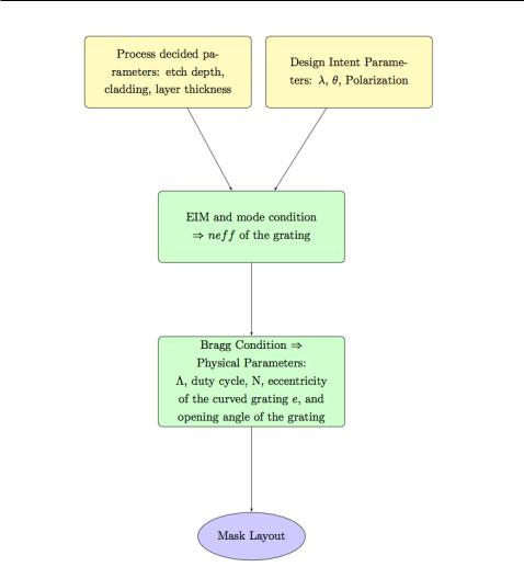
The design ow of the proposed design method is shown in the ow chart on the next page. For any speci c grating coupler there are two types of input parameters: process determined parameters and design intent parameters. The process determined parameters include the etch depth, the cladding material, and the thickness of each layer, which are determined by the fabrication process and wafer type. The design intent parameters include central wavelength, , incident angle, , and the polarization of the operational wave.
41
3.2. Universal Grating Coupler Design
Figure 3.16: Flow chart of the universal design method
42

3.2. Universal Grating Coupler Design
Knowning the cladding material, the thickness of the top silicon layer, and the etch depth, we can obtain the e ective index of the grating teeth and the e ective index of the grating slots using the EIM, under the assumption that the grating has a in nite width. This assumption holds under the condition that grating couplers for an optical bre normally have widths of more than 12 microns, which is much larger than the central wavelength. If we denote the e ective index of the grating tooth to be ne 1, and the e ective index of refraction of the grating slots to be ne 2, then the e ective index of the grating can be expressed as:
ne = ff ne 1 + (1 ff) ne 2 |
(3.7) |
where ff denotes the ll factor of the grating, which is de ned as the ratio of the duty cycle and the grating period, i.e., ff = w= .
After obtaining the e ective index ne of the grating, the Bragg condition is employed to calculate the grating period:
nc sin = ne m |
|
(3.8) |
|
where nc denotes the e ective index of the bre mode in the cladding, is the incident angle, is the desired central wavelength, and m denotes the di raction order. For a speci c grating coupler nc, , and are known. In addition, the e ective index of the grating ne can be calculated by the EIM. Therefore, we can get the period of the grating from Equation 3.18. This method is used to design a one-dimensional coupler, which can be simulated by 2D simulations in FDTD.
3.2.2Simulation Results
Simulation models have been built using FDTD Solutions (Scripts shown in Appendix A). Given the process determined parameters and design intent parameters, our model can generate the desired grating couplers and simulate them. The input parameters used in our case are listed in Table 3.3.
Extensive simulations have been done for the wavelengths ranging from
43

3.2. Universal Grating Coupler Design
Top Si thickness |
Etch depth |
Cladding |
|
|
Polarization |
|
|
|
|
|
|
|
|
|
|
|
|
220 nm |
70nm |
air/oxide |
1550 nm |
10 degree |
TE/TM |
Table 3.3: Input paramters
1260nm to 1675nm, which covers all of the six optical bands. Air cladding and SiO2 cladding have been examined for both TE and TM waves to verify the accuracy of the universal design method. The input parameters used in our case are shown in Table 3.3. Figure 3.17 shows the simulation results of the grating couplers for TE light with a 10 degree incident angle and SiO2 as the cladding. The x-axis denotes the designed central wavelength, . The left y-axis, indicated by the blue curve, denotes the insertion loss of the grating couplers generated by the model, and the right y-axis, indicating by the green curve, denotes the wavelength mismatches. The wavelength mismatch, , is de ned as the di erence between the actual central wavelength,
real, obtained from FDTD simulations and the design intent wavelength,, i.e., = real . The insertion loss of the grating couplers varies as the wavelength changes, which results from the phase condition changes between Pre ection3 and Pre ection4 as shown in Fig. 3.6. Constructive interferences is obtained between Pre ection3 and Pre ection3 around 1310nm and 1550nm, therefore, the insertion losses of the grating couplers around these wavelengths are smaller. However, destructive interference between Pre ection3 and Pre ection4 is obtained around 1400nm, therefore, the insertion loss of the grating couplers around these wavelengths are larger. For most wavelengths, the simulated central wavelengths are close to the designed central wavelengths, especially around the two most commonly used optical windows around 1310 nm and 1550 nm. The wavelength mismatch can be calibrated by adjusting the incident angle during the measurement or by compensating for the wavelength during the design stage. Given that the tuning coe cient is 7 nm=degree for TE light and 10 nm=degree for TM light, the wavelength mismatches are within 2 degrees in most cases.
Figure. 3.18 shows the simulation results of the grating couplers for TM light with a 10 degree incident angle and SiO2 as the cladding. The wave-
44

3.2. Universal Grating Coupler Design
length mismatches of grating couplers for TM light are larger than that of the grating couplers for TE light at some wavelengths. This is the case because the TM modes are less con ned within the waveguides, therefore, the central wavelengths of the grating couplers for TM light are more sensitive to refractive index change than the central wavelengths of the grating couplers for TE light.
For comparison purposes, we simulated the grating couplers generated by the universal design model with a 10 degree incident angle and employed air as the cladding. Figure 3.19 shows the simulation results of the grating couples for TE operation with a 10 degree incident angle and air as the cladding. Figure 3.20 shows the simulation results of the grating couplers for TM operation with a 10 degree incident angle and air as the cladding. The insertion loss of the grating couplers with SiO2 as the cladding are smaller than the ones with air cladding. This is the case because the refractive index contrast between the air and the top Si layer is reduced by employing the cladding layer, therefore, more light can be coupled into the grating by choosing the right thickness for the cladding layer. Also, the cladding layer mitigates the refractive index change of the grating as the period and the duty cycle of the grating varies, which results in the central wavelength being less sensitive to the changes in the duty cycle and grating period.
45
3.2. Universal Grating Coupler Design
|
−2 |
|
|
|
|
5 |
|
|
−3 |
|
|
|
|
0 |
(nm) |
|
|
|
|
|
|
|
|
power (dB) |
−4 |
|
|
|
|
−5 |
wavelength mismatch |
−5 |
|
|
|
|
−10 |
||
−6 |
|
|
|
|
−15 |
||
|
|
|
|
|
|
||
|
−7 |
1300 |
1400 |
1500 |
1600 |
−20 |
|
|
1200 |
1700 |
|
||||
|
|
|
wavelength (nm) |
|
|
|
|
Figure 3.17: Universal grating couplers with 10 degree incident angle for TE mode wave with oxide cladding
−2 |
|
|
|
|
|
|
|
|
50 |
|
|
|
|
|
|
|
|
|
(nm) |
−4 |
|
|
|
|
|
|
|
|
0 |
power(dB) |
|
|
|
|
|
|
|
|
wavelengthmismatch |
−6 |
1300 |
1350 |
1400 |
1450 |
1500 |
1550 |
1600 |
1650 |
−50 |
1250 |
1700 |
wavelength (nm)
Figure 3.18: Universal grating couplers with 10 degree incident angle for TM mode wave with oxide cladding
46