

Много теории
.pdfList of Figures
3.22 Mask layout of a grating coupler with focusing grating curve 50
3.23Measurement vs. simulation of universal grating couplers
with 10 degree incident angle . . . . . . . . . . . . . . . . . . 52
3.24Measurement vs. simulation of universal grating couplers
with 15 degree incident angle . . . . . . . . . . . . . . . . . . 52
3.25Measurement vs. simulation of universal grating couplers
with 20 degree incident angle . . . . . . . . . . . . . . . . . . 53
3.26(a) Peak power of simulation and measurement results with 10 incident angle; (b)comparison of simulated and measured
wavelength mismatch with 10 degree incident angle . . . . . . 54
3.27(a)Peak power of simulation and measurement results with 15 incident angle; (b)comparison of simulated and measured
wavelength mismatch with 15 degree incident angle . . . . . . 54
3.28(a)Peak power of simulation and measurement results with 20 incident angle; (b)comparison of simulated and measured
wavelength mismatch with 20 degree incident angle . . . . . . 55
4.1Schematic of fully etched grating coupler . . . . . . . . . . . . 57
4.2Schematic of di raction, re ection and penetration of a reg-
ular fully etched grating coupler . . . . . . . . . . . . . . . . 58
4.3Insertion loss of grating couplers with 20 degree incident angle for TE operation wave as function of the thickness of the
buried oxide. . . . . . . . . . . . . . . . . . . . . . . . . . . . 59
4.4Directionality, insertion loss and re ection to waveguide of a general fully-etched grating coupler . . . . . . . . . . . . . . . 61
4.5Mask layout of a fully etched grating coupler test structure . 62
4.6Comparison of measurement result and simulation result of fully-etched grating coupler . . . . . . . . . . . . . . . . . . . 63
4.7Comparison of back re ections between shallow-etched grat-
ing coupler and fully-etched grating coupler . . . . . . . . . . 64
4.8Schematic of a fully etched grating coupler with sub-wavelength gratings . . . . . . . . . . . . . . . . . . . . . . . . . . . . . . 66
xi

List of Figures
4.9Comparison of regular fully etched grating coupler and the fully etched grating coupler with minor sub-wavelength grat-
ings. . . . . . . . . . . . . . . . . . . . . . . . . . . . . . . . . 67
4.10Measurement results of the regular fully etched grating coupler and the fully-etched grating coupler with minor sub-
wavelength gratings . . . . . . . . . . . . . . . . . . . . . . . |
68 |
5.1 Diagram of wave vectors for vertical grating coupler . . . . . |
71 |
5.2Insertion loss and back re ection of a regular vertical grating
coupler . . . . . . . . . . . . . . . . . . . . . . . . . . . . . . 72
5.3Schematic of bidirectional grating coupler for vertical coupling 73
5.4 Cross section of a bidirectional grating coupler . . . . . . . . 74
5.5The insertion loss of the optimized bidirectional grating coupler 75
5.6Insertion of the bidirectional vertical grating coupler as func-
tion of wavelength for di erent o set . . . . . . . . . . . . . . 76
5.7Schematic of a bidirectional grating coupler with incident wave o from the centre of the grating. . . . . . . . . . . . . . 77
xii
Acknowledgements
I would like to thank my supervisor Dr. Lukas Chrostowski. For the care he provided to help me settle down when I rst came to the University of British Columbia as an international student, for the patient guidance and help he provided when I was faced with di culties and for the friendly and warm atmosphere he has created within our research group.
I would like also to thank Dr. Nicolas Jaeger for the helpful instruction and kindly help with my research.
Also, I would like to thank my colleagues Wei Shi, Xu Wang, Han Yun, Jonas Flueckiger, Samantha Grist, Charlie Lin, and Sahba Talebi Fard. Special thanks to Wei Shi for his instructive discussions and kind help.
In addition, I would also like to acknowledge the nano-fabrication center at University of Washington, CMC Microsystems and OpSIS IME for the fabrication of my devices and Lumerical Solutions Inc. for their technical support.
xiii
Dedication
To my father Junping Wang and my mother Miaoling Zhang, who have shown me what love is. Speci cally, the courage, determination and passion from my father to help me nd what I truly love and to follow my own heart, and the rationality from my mother, which helped me to think independently when I met obstacles in my life. To my ance Ge Shi, for her dedication and love.
xiv
Chapter 1
Introduction
1.1Silicon Photonics
After dominating the electronics industry for decades, silicon is on the verge of becoming the material of choice for the photonics industry [21]. The early work in the area of silicon photonics dates back to the late 1980s and the early 1990s [12, 20, 43, 46, 51, 52, 52, 53, 62]. The motivation for silicon photonics is its compatibility with the silicon Integrated Circuit (IC) manufacturing process, which represents the most spectacular convergence of technological sophistication and economies of scale. The industry is able to produce microprocessors with hundreds of millions of components, all integrated onto a thumb-size chip, and to o er them at extremely low price.
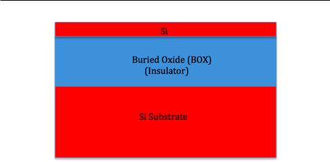
Another motivation is the availability of high-quality silicon-on-insulator (SOI) wafers, an ideal platform for creating planar waveguide circuits. A schematic of an SOI wafer is shown in Fig. 1.1. An SOI wafer consists of three layers: a silicon substrate at the bottom (of Fig. 1.1) for mechanical support, a buried oxide (BOX) layer (in the middle) acting as the insulator layer, and another silicon layer (on the top) acting as the functional wave guiding layer. There may be another cladding layer on top of the silicon layer for protection. The strong optical con nement o ered by the high index contrast between Si
(n=3.45) and SiO2(n = 1.45) makes it possible to make photonics devices on the scale of a few hundred nanometers. Such small dimensions are required for compatibility with the IC processing. The Smart Cut [2] technology commercialized by Soitec also propelled the commercial applications of SOI into exponential growth and entered the mainstream of Ultra Large Scale Integration (ULSI).
1
1.1. Silicon Photonics
Figure 1.1: Schematic of SOI wafer
The main application envisioned for silicon photonics is optical interconnects for CMOS electronics [34]. Conventional wisdom holds that optical interconnects are much better suited than copper interconnects in handling high data rates. The physical bene ts of changing the technology used for interconnects to silicon photonic chips in computing and switching systems have been detailed in [33]. With the advantages of design simpli - cation, architectural advantages and physical bene ts such as reduction of power dissipation in interconnects and voltage isolation etc., light beams that have dominated long-distance communication are progressively taking over in shorter distance networks. Luxtera announced the world's rst 40 Gigabit Optical Active Cable (OAC) in 2007 [28]. Intel demonstrated their 4x12.5 Gbps CWDM silicon photonics link using integrated hybrid silicon lasers [25, 37] in 2010. IBM unveiled the holey optochip to transfer information at terabit per second speed in 2012 [10]. All those advancess show the potential of silicon photonics as the future solution for optical interconnects.
Another important application of silicon photonics is bio-sensing. A disposable mass-produced sensor would be attractive as it could grow the market for biosensors. Sensor applications are somewhat di erent from optical communication ones as there are other low cost optical technologies that
2

1.2. Challenge of Coupling Light Into Nanophotonic Waveguide
compete in this space [23]. One likely application area for silicon photonics is the so-called lab-on-a-chip, in which both reaction and analysis are performed in a single device. In the future, this could be extended to include electronic intelligence and wireless communications to create intelligent sensor networks for environmental monitoring [21].
In addition, silicon has material properties that are important for a new class of mid-infrared (IR) photonics devices. These include the linear and non-linear optical properties in the mid-wave IR spectrum. The high optical intensity arising from the large index contrast (between Si and SiO2) makes it possible to observe nonlinear optical interactions, such as Raman and Kerr e ects, in chip-scale devices. Far from being limited to the near-IR data communication band, from 1.26 to 1.67 microns, silicon also has a low loss wavelength window extending from 1.1 to nearly 7 microns [22]. But oxide limits its use in SOI to 3 microns. Silicon has high thermal conductivity (10x higher than GaAs), high optical damage threshold (10x higher than GaAs), and high third-order optical nonlinearities [21].
1.2Challenge of Coupling Light Into Nanophotonic Waveguide
Due to the large refractive index contrast between the silicon core (n 3.47 at 1550 nanometers) and the silicon dioxide cladding (n 1.5 at 1550 nanometers), propagation modes are highly con ned within the waveguide with a dimension on the order of a few hundred nanometers, which enables largescale integration. However, the small feature size of the waveguide raises the problem of huge mode mismatch between the optical mode within an optical bre and the mode within the waveguide. The cross-sectional area of an optical bre-core (with a diameter of 10 microns) is almost 3,000 times larger than that of a silicon waveguide (with dimensions of 500 nanometers x 220 nanometers).
Several approaches have been demonstrated to tackle the problem of mode mismatch. Edge coupling using spot size converters and lensed -
3
1.2. Challenge of Coupling Light Into Nanophotonic Waveguide
bres is one solution used to address this, and high-e ciency coupling with an insertion loss below 0.5 dB has been demonstrated [30]. However, this approach can be only used at the edge of the chips, and the implementation of such designs requires complicated post-processes, which increase the packaging cost dramatically. The alignment of such devices during the measurement requires high accuracy, which often takes a lot of e ort.
The grating couplers are an alternative solution to tackle the issue of mode mismatch. Compared to the edge coupling, grating couplers have several advantages: alignment to grating couplers during measurement is much easier than alignment to edge couplers; the fabrication of grating couplers does not require post-processing, which reduces the fabrication cost; grating couplers can be put anywhere on a chip, which provides exibility in the design as well as enabling wafer scale automated testing. Both academic and industrial research groups have demonstrated high e ciency grating couplers [32, 35, 41].
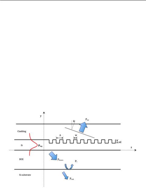
Figure 1.2: Schematic of grating coupler
4

1.3.Grating Coupler
1.3Grating Coupler
Figure 1.2 is a schematic of a shallow-etched grating coupler design in silicon- on-insulator. The thickness of the functional Si layer and the thickness of the buried oxide (BOX) layer are determined by the wafer type. A cladding layer is often employed to protect the functional silicon layer, as shown in Fig. 1.2. However, for some uses such as bio-sensing, air cladding is required. In Fig. 1.2 :
denotes the grating period, which represents the length of the periodic pattern;
W denotes duty cycle of the grating coupler, which is the width of the grating tooth;
ff denotes ll factor, which is de ned as the ratio of the grating period and the duty cycle, i.e, ff = =W ;
denotes the incident angle of the grating coupler, which is the angle between the incident wave and the normal to the grating surface;
ed denotes the heights of the grating teeth, which are de ned as etch depth.
In addition to the geometric variables de ned above, some other terms are often used when discussing grating couplers:
1.Directionality: the ratio between the power di racted upwards (Pup) and the input power from the waveguide (Pwg) [35], which is usually expressed in decibels (dB) as 10 log10(Pup=Pwg);
2.Insertion loss (coupling e ciency): the ratio between the power coupled into the fundamental mode of the bre (Pfund) and the input power from the waveguide (Pwg), which is usually expressed in dB as
10 log10(Pfund=Pwg);
3.Penetration loss: the ratio between the power lost in the substrate (Psub) and the input power from the waveguide, which is usually expressed in dB as 10 log10(Psub=Pwg);
5
1.4.Slab Waveguide and Channel Waveguide
4.Back re ection to the waveguide: due to the refractive index contrast between the silicon wire waveguide and the grating, part of the input light from the waveguide will be re ected back into the waveguide. The ratio between the re ected power and the input power from the waveguide is called back re ection to the waveguide. It is usually expressed in dB or in percentage. This back re ection is unwanted because it will cause Fabry-Perot oscillations by re ecting back and forth between the input and output grating couplers [35, 55].
1.4Slab Waveguide and Channel Waveguide
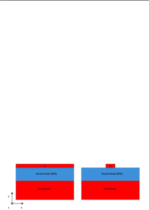
At angles of incidence above the critical angle it is possible to achieve total internal re ection from a dielectric interface given that the incident electromagnetic wave is in the medium with the higher refractive index. So, it should be possible to place a slab of dielectric with a high refractive index between two media with lower refractive indices and con ne a plane wave to propagate in the high index dielectric slab [19]. Such a waveguide is called the slab waveguide. A schematic of a slab waveguide in SOI is shown in the left side of Fig. 1.3. The slab is such that it extends to in nity in the x and z directions. However, the waveguide used in photonic systems are the ones with two-dimensional refractive index pro les, which is shown in the right side of Fig. 1.3. Such a waveguide is called the channel waveguide.
Figure 1.3: Schematic of slab waveguide and channel waveguide in SOI
6