

Много теории
.pdf3.2. Universal Grating Coupler Design
−2 |
|
|
|
|
20 |
|
−4 |
|
|
|
|
0 |
(nm) |
|
|
|
|
wavelength mismatch |
||
−6 |
|
|
|
|
−20 |
|
power(dB) |
|
|
|
|
|
|
−8 |
1300 |
1400 |
1500 |
1600 |
−40 |
|
1200 |
1700 |
|
||||
|
|
wavelength (nm) |
|
|
|
|
Figure 3.19: Universal grating coupler with 10 degree incident angle for TE mode wave with air cladding
−3 |
|
|
|
|
10 |
|
−4 |
|
|
|
|
0 |
|
−5 |
|
|
|
|
−10 |
(nm) |
|
|
|
|
wavelengthmismatch |
||
−6 |
|
|
|
|
−20 |
|
−7 |
|
|
|
|
−30 |
|
power(dB) |
|
|
|
|
|
|
−8 |
|
|
|
|
−40 |
|
−9 |
1300 |
1400 |
1500 |
1600 |
−50 |
|
1200 |
1700 |
|
||||
|
|
wavelength (nm) |
|
|
|
|
Figure 3.20: Universal grating coupler with 10 degree incident angle for TM mode wave with air cladding
47
3.2. Universal Grating Coupler Design
|
−2 |
|
|
|
|
|
|
−3 |
|
|
|
|
|
|
−4 |
|
|
|
|
|
(dB) |
−5 |
|
|
|
|
|
|
|
|
|
|
|
|
power |
−6 |
|
|
|
|
|
|
|
|
|
|
|
|
|
−7 |
|
|
|
|
|
|
−8 |
|
|
Optimized |
|
|
|
|
|
|
|
|
|
|
−9 |
|
|
UGC |
|
|
|
1520 |
1540 |
1560 |
1580 |
1600 |
|
|
1500 |
|||||
|
|
|
wavelength (nm) |
|
|
|
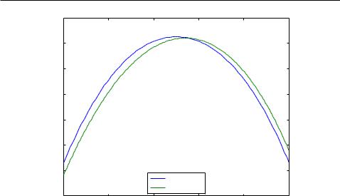
Figure 3.21: Comparison of designs generated by universal grating coupler model and the optimized design for 1550nm TE wave with 10 degree incident angle
In order to see the accuracy of the universal grating coupler design method, we picked the most commonly used wavelength in telecommunications, i.e., 1550 nm, to compare the spectrum of the grating coupler generated by the universal design model and the spectrum of the grating coupler design optimized by FDTD simulation. Figure. 3.21 shows the comparison of the simulation results of the grating coupler generated by the universal design method and the grating coupler optimized by FDTD simulations. The green dash curve denotes the spectrum of the grating coupler generated by the universal design method, which has an insertion loss of -2.79 and a 3dB bandwidth of 78.8 nm, and the blue curve denotes the spectrum of the grating coupler design optimized by FDTD simulations, which has an insertion loss of -2.74 and a 3dB bandwidth of 79.8 nm. The central wavelength mismatch between the two grating couplers is as small as 3 nanometers and the insertion loss only improved by 1% after hundreds of simulation sweeps for di erent design variables. In this thesis, the optimization of the grat-
48

3.2. Universal Grating Coupler Design
ing coupler we use only considered uniform gratings. The improvements in the insertion loss can be obtained by more sophisticated designs with non-uniform gratings [50].
3.2.3Mask Layout
With the physical parameters calculated from the Bragg condition, we can generate the mask layout of the grating coupler. So far, we have only addressed the grating couplers with straight gratings. For those grating couplers, two dimensional tapers are required to convert the mode from the grating into the waveguide. Typically, the width of the grating is about 12 microns, and the width of the waveguide is only about 500 nanometers. To achieve lossless conversion between the grating and the waveguide, two dimensional tapers with a length on the order of a few hundred microns are required [56], which is not space e cient. To tackle this issue, curved grating designs have been employed to make the grating couple more compact [54]. According to [54], compact grating structure can be obtained by curving the grating lines following the equation:
p
q 0 = ne y2 + z2 zntcos( c) (3.9)
where q is the integer indicating each grating lines, c denotes the angle between the bre and the chip surface, nt denotes the refractive index of the environment, 0 denotes the central wavelength, and ne denotes the e ective index of the grating. The expression of Bragg condition for the curved gratings can be also converted to a cylindrical system [32]:
nekr = nckrsin( )cos( ) + 2 N |
(3.10) |
where ne denotes the e ective of the mode propagating inside the grating, k denotes the wave vector in free space, nc denotes the e ective index of the wave in the cladding, denotes the incident angle, and denotes the angle subtended by an arbitrary points on the grating and to the z-axis. We generated a universal script in Pyxis (shown in Appendix B), a commercial
49
3.2. Universal Grating Coupler Design
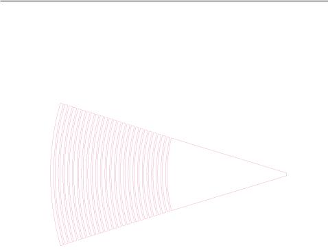
software from Mentor Graphics, to draw the mask layout of the desired grating couplers with curved gratings. Our script is based on the cylindrical expression of the curved grating as shown by Equation. 3.10. An example of the mask layout of the grating coupler generated by our model is shown in Fig. 3.22.
Figure 3.22: Mask layout of a grating coupler with focusing grating curve
3.2.4Measurement Results
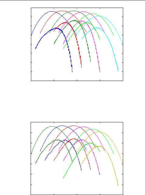
Test structures of the grating couplers generated by the universal design method have been fabricated through the electron beam lithography at University of Washington using the JEOL JBX-6300FS E-Beam Lithography system. Standard SOI wafer with a 220-nanometer top silicon layer and a 2-micron buried oxide were used for the fabrication. Silicon oxide was employed as the cladding layer to protect the functional structures. The etch depth of the shallow etched grating couplers is 70 nanometers. The grating couplers were designed for TE mode wave with incident angles of 10 degree, 15 degree and 20 degree. The target central wavelengths are 1500nm, 1520nm, 1540nm, 1560nm, 1580nm, and 1600nm.
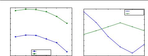
Figure 3.23 shows the simulated and measured spectra of the grating couplers generated by the universal design method with a 10 degree incident
50

3.2. Universal Grating Coupler Design
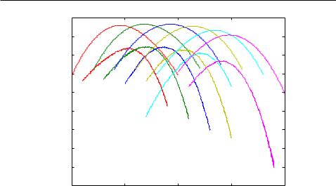
angle. The simulation and measurement results of the grating couplers with the same central wavelength are indicated by the same colour. Due to the misalignment, inevitable system loss and fabrication errors, the measured insertion loss of the grating couplers are larger than the simulated results. In addition, the bandwidths of the measured grating coupler are narrower than the simulated ones, which is hypothesized to be originating from the large air gap. Similarly, Figure 3.24 shows the simulated and measured spectra of the grating couplers generated by the universal design method with a 15 degree incident angle, and Fig. 3.25 shows the simulated and measured spectra of the grating couplers generated by the universal design method with a 20 degree incident angle. The spectra of the measurement results follows the same trend as the simulation results but with the addition of extra insertion loss. The mismatch in central wavelength between the simulation results and measurement results may caused by the fabrication errors,e.g., the possible fabrication errors in grating period, duty cycle, and the thickness variation of the Si layer across the samples. The sensitivity of central wavelength of the design as function of design parameters such as grating period, duty cycle etc have been shown in Table 3.4, which has been explained in the previous section.
Parameters |
period |
duty cycle |
etch depth |
incident angle |
|
|
|
|
|
|
|
|
|
|
Tuning coe cient |
1.4 |
0.215 |
1.9 |
7 nm=degree |
|
|
|
|
|
Table 3.4: Tuning coe cient of di erent parameters
51
3.2. Universal Grating Coupler Design
|
−2 |
|
|
|
|
|
−4 |
|
|
|
|
|
−6 |
|
|
|
|
(dB) |
−8 |
|
|
|
|
−10 |
|
|
|
|
|
Power |
|
|
|
|
|
−12 |
|
|
|
|
|
|
|
|
|
|
|
|
−14 |
|
|
|
|
|
−16 |
|
|
|
|
|
−18 |
1500 |
1550 |
1600 |
1650 |
|
1450 |
||||
|
|
|
Wavelength (nm) |
|
|
Figure 3.23: Measurement vs. simulation of universal grating couplers with 10 degree incident angle
|
−2 |
|
|
|
|
|
−4 |
|
|
|
|
|
−6 |
|
|
|
|
(dB) |
−8 |
|
|
|
|
|
|
|
|
|
|
Power |
−10 |
|
|
|
|
|
|
|
|
|
|
|
−12 |
|
|
|
|
|
−14 |
|
|
|
|
|
−16 |
1500 |
1550 |
1600 |
1650 |
|
1450 |
||||
|
|
|
Wavelength (nm) |
|
|
Figure 3.24: Measurement vs. simulation of universal grating couplers with 15 degree incident angle
52
3.2. Universal Grating Coupler Design
|
−2 |
|
|
|
|
|
−4 |
|
|
|
|
|
−6 |
|
|
|
|
(dB) |
−8 |
|
|
|
|
−10 |
|
|
|
|
|
Power |
−12 |
|
|
|
|
−14 |
|
|
|
|
|
|
|
|
|
|
|
|
−16 |
|
|
|
|
|
−18 |
|
|
|
|
|
−20 |
1500 |
1550 |
1600 |
1650 |
|
1450 |
||||
|
|
|
Wavelength (nm) |
|
|
Figure 3.25: Measurement vs. simulation of universal grating couplers with 20 degree incident angle
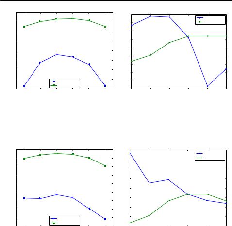
Further comparison of simulation and measurement results of the grating couplers generated by the universal design method are shown in Fig. 3.26 to Fig. 3.28. Figure. 3.26 (a) shows the comparison of the simulated and measured insertion loss of the grating couplers with 10 degree incident angle. Figure. 3.26 (b) shows the comparison of the simulated and measured central wavelength mismatch. Similarly, the comparison between simulation and measurement results of the grating couplers with 15 degree incident angle and 20 degree incident angle are shown in Fig. 3.27 to Fig. 3.28. Obviously, the insertion loss of the simulation results and measurement results follows the same trends. However, the central wavelength mismatch of the measurement results shows a random behaviour, which is not consistent with the simulation results. The discrepancy in central wavelength is mainly caused by the fabrication error because the possible fabrication errors in grating period, duty cycle, etch depth all have impacts on the central wavelength of the grating coupler.
53
|
|
|
3.2. Universal Grating Coupler Design |
|
|
|
|||||||
|
−2.5 |
|
|
|
|
|
|
6 |
|
|
|
|
|
|
|
|
|
|
|
|
|
|
|
|
measurement |
||
|
|
|
|
|
|
|
|
|
|
|
|
||
|
−3 |
|
|
|
|
|
|
4 |
|
|
|
simulation |
|
|
−3.5 |
|
|
|
|
|
(nm) |
2 |
|
|
|
|
|
|
|
|
|
|
|
|
0 |
|
|
|
|
|
|
(dB)power |
−5.5 |
|
|
|
|
|
mismatchwavelength |
|
|
|
|
|
|
|
−4 |
|
|
|
|
|
|
|
|
|
|
|
|
|
−4.5 |
|
|
|
|
|
|
−2 |
|
|
|
|
|
|
|
|
|
|
|
|
|
|
|
|
|
|
|
|
|
|
|
|
|
|
|
−4 |
|
|
|
|
|
|
−5 |
|
|
|
|
|
|
|
|
|
|
|
|
|
|
|
|
|
|
|
|
−6 |
|
|
|
|
|
|
|
|
|
|
|
|
|
−8 |
|
|
|
|
|
|
−6 |
|
measurement |
|
|
|
−10 |
|
|
|
|
|
|
|
|
|
|
|
|
|
|
|
|
|
|||
|
−6.5 |
|
simulation |
|
|
|
−12 |
|
|
|
|
|
|
|
1520 |
1540 |
1560 |
1580 |
1600 |
|
1520 |
1540 |
1560 |
1580 |
1600 |
||
|
1500 |
|
1500 |
||||||||||
|
|
|
wavelength (nm) |
|
|
|
|
|
wavelength (nm) |
|
|
||
(a) |
(b) |
Figure 3.26: (a) Peak power of simulation and measurement results with 10 incident angle; (b)comparison of simulated and measured wavelength mismatch with 10 degree incident angle
|
−2.5 |
|
|
|
|
|
|
10 |
|
|
|
measurement |
|
|
|
|
|
|
|
|
|
|
|
|
|
||
|
−3 |
|
|
|
|
|
|
8 |
|
|
|
simulation |
|
|
|
|
|
|
|
|
|
|
|
|
|
|
|
|
−3.5 |
|
|
|
|
|
(nm) |
6 |
|
|
|
|
|
|
|
|
|
|
|
|
|
|
|
|
|
||
|
|
|
|
|
|
|
|
|
|
|
|
|
|
(dB)power |
−4 |
|
|
|
|
|
mismatchwavelength |
−2 |
|
|
|
|
|
|
|
|
|
|
|
|
|
4 |
|
|
|
|
|
|
−4.5 |
|
|
|
|
|
|
|
|
|
|
|
|
|
−5 |
|
|
|
|
|
|
2 |
|
|
|
|
|
|
|
|
|
|
|
|
|
|
|
|
|
|
|
|
−5.5 |
|
|
|
|
|
|
0 |
|
|
|
|
|
|
|
|
|
|
|
|
|
|
|
|
|
|
|
|
−6 |
|
|
|
|
|
|
|
|
|
|
|
|
|
−6.5 |
|
measurement |
|
|
|
−4 |
|
|
|
|
|
|
|
−7 |
|
simulation |
|
|
|
−6 |
|
|
|
|
|
|
|
1520 |
1540 |
1560 |
1580 |
1600 |
|
1520 |
1540 |
1560 |
1580 |
1600 |
||
|
1500 |
|
1500 |
||||||||||
|
|
|
wavelength (nm) |
|
|
|
|
|
wavelength (nm) |
|
|
||
(a) (b)
Figure 3.27: (a)Peak power of simulation and measurement results with 15 incident angle; (b)comparison of simulated and measured wavelength mismatch with 15 degree incident angle
54
|
|
|
3.2. Universal Grating Coupler Design |
|
|
|
|||||||
|
−2.5 |
|
|
|
|
|
|
6 |
|
|
|
|
|
|
|
|
|
|
|
|
|
|
|
|
measurement |
||
|
−3 |
|
|
|
|
|
|
|
|
|
|
||
|
|
|
|
|
|
|
4 |
|
|
|
simulation |
|
|
|
−3.5 |
|
|
|
|
|
(nm) |
2 |
|
|
|
|
|
|
|
|
|
|
|
|
|
|
|
|
|
||
|
−4 |
|
|
|
|
|
0 |
|
|
|
|
|
|
|
|
|
|
|
|
mismatchwavelength |
|
|
|
|
|
||
(dB)power |
|
|
|
|
|
|
|
|
|
|
|
||
−4.5 |
|
|
|
|
|
−2 |
|
|
|
|
|
||
|
|
|
|
|
|
|
|
|
|
|
|
||
|
|
|
|
|
|
|
|
|
|
|
|
|
|
|
−5 |
|
|
|
|
|
|
−4 |
|
|
|
|
|
|
−5.5 |
|
|
|
|
|
|
−6 |
|
|
|
|
|
|
−6 |
|
|
|
|
|
|
−8 |
|
|
|
|
|
|
−6.5 |
|
measurement |
|
|
|
−10 |
|
|
|
|
|
|
|
−7 |
|
simulation |
|
|
|
−12 |
|
|
|
|
|
|
|
1520 |
1540 |
1560 |
1580 |
1600 |
|
1520 |
1540 |
1560 |
1580 |
1600 |
||
|
1500 |
|
1500 |
||||||||||
|
|
|
wavelength (nm) |
|
|
|
|
|
wavelength (nm) |
|
|
||
(a) (b)
Figure 3.28: (a)Peak power of simulation and measurement results with 20 incident angle; (b)comparison of simulated and measured wavelength mismatch with 20 degree incident angle
55
Chapter 4
Fully Etched Grating
Coupler
All of the grating couplers mentioned so far are shallow etched grating couplers, and the fabrication of these grating couplers requires two lithography steps. Shallow etched grating couplers have the advantage of smaller back re ection to the waveguide and lower insertion loss than the fully etched grating couplers. However, the additional lithography step also increases the fabrication cost and complexity. Fully etched grating couplers o er a fast and economic experimental solution for the coupling issue, especially for quick prototyping through electron beam lithography. All of the fundamental building blocks of the photonics integrated circuits can be fabricated in just one step by implementing the fully etched grating coupler. In this chapter, the performance of the traditional fully etched grating couplers will be presented rst, and the drawbacks of which will be pointed out. Then, fully etched grating couplers with refractive index engineered subwavelength structures will be introduced to improve the performance of the fully etched grating couplers.
4.1Regular Fully Etched Grating Coupler
Figure 4.1 is a schematic of a regular fully etched grating coupler in SOI with uniform gratings. The grating teeth are formed by fully etching through the functional silicon layer instead of partially etching. The thicknesses of the functional silicon layer and buried oxide used in our case are 2 um and 220 nm, respectively. Air is employed as the cladding for the grating coupler design.
56