

Много теории
.pdf4.1. Regular Fully Etched Grating Coupler
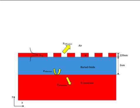
Figure 4.1: Schematic of fully etched grating coupler
4.1.1Bottlenecks of Regular Fully Etched Grating Couplers
The disadvantages of the regular fully etched grating couplers include the poor insertion loss and the large back re ection to the waveguide. The poor insertion loss is mainly caused by the mode mismatch and penetration loss, and the large back re ection to the waveguide results from the large refractive index contrast between the waveguide and the grating.
When considering the grating coupler as an output coupler (shown in Fig. 4.1), the power in the waveguide will be exponentially decaying due to the presence of the grating [49]:
Pwg(z) = Pwg(z = 0)exp( 2 z) |
(4.1) |
where 2 is the coupling strength or leakage factor of the grating, Pwg(z) denotes the power of the mode at z. The inverse of the coupling strength is de ned as the coupling length, i.e., Lc = (2 ) 1. For shallow etched grating couplers, the coupling strength is small, and the coupling length Lc of the grating couplers is similar to the diameter of the mode from an opticalbre. Therefore, a large mode overlap between the exponential mode from the grating and the Gaussian mode of a bre can be achieved. However,
57
4.1. Regular Fully Etched Grating Coupler
the coupling strength of fully etched grating couplers is much larger than that of the shallow etched ones, therefore the coupling length Lc of the fully etched grating couplers is much smaller than that of the shallow etched ones, which results in a larger mode mismatch between the grating and the opticalbre.
Figure 4.2: Schematic of di raction, re ection and penetration of a regular fully etched grating coupler
The large penetration loss is another reason leading to the poor insertion loss of the fully etched grating couplers. Figure 4.2 shows the di raction, re ection, and penetration behaviours of a fully etched grating coupler. As the incident wave impinges on the gratings, a portion of the light is di racted upwards to the air and a potion of the light is scattered downward to the substrate. At the interface of the buried oxide and the Si substrate, part of the light scattered downward from the grating is re ected back to the grating and the other part of the light penetrates into the substrate. At the interface of the functional Si layer and the buried oxide, the re ected light from the lower interface interferes with the portion of light di racted upwards. Depending on the phase condition, either constructive interference or destructive interference can be obtained. Lowest insertion loss can be achieved when constructive interference is obtained.
58
4.1. Regular Fully Etched Grating Coupler
|
−3 |
|
|
−4 |
|
(dB) |
−5 |
|
|
||
Loss |
−6 |
|
|
||
Insertionl |
−7 |
|
−8 |
||
|
||
|
−9 |
|
|
Fully etched GC |
|
|
Shallow etched GC |
|
|
−10 |
1 |
1.5 |
2 |
2.5 |
3 |
|
Thickness of the buried oxide (um) |
|
||
Figure 4.3: Insertion loss of grating couplers with 20 degree incident angle for TE operation wave as function of the thickness of the buried oxide.
The phase condition between the di racted wave, i.e., Pdi raction, and the re ected wave, i.e., Pre ected, depends on the thickness of the buried oxide. Figure 4.3 shows the insertion loss of grating couplers with 20 degree incident angles for TE operation wave as function of the thickness of the buried oxide. As we vary the thickness of the buried oxide from 1 um to 3 um, the insertion loss of the grating couplers varies as the phase conditions changes. The standard SOI wafers normally have a 2-um thick buried oxide, which is chosen for the shallow etched grating couplers, but not ideal for fully etched grating couplers.
The large back re ection to the waveguide of the fully etched grating couplers results from the Fresnels re ection. The re ection coe cient for TE wave can be expressed as:
rT E = |
n1 |
cos( i) n2 cos( t) |
(4.2) |
|
|
||||
n1 |
cos( i) + n2 cos( t) |
|||
|
|
59

4.1. Regular Fully Etched Grating Coupler
where n1, n2 are the refractive indices of corresponding layers. And i , t are the incident angle and transmission angle, respectively. In our case, n1 equals to the refractive index of silicon, i.e., n1 = 3:47, and n2 equals to the refractive index of cladding material. The Fresnels re ection coe cient is as high as 0.414 in the case with silica as cladding material, which means more than 17% of the power will be re ected back into the waveguide. The back re ection to waveguide is even larger in the case with air as cladding since air has a lower refractive index than silica.
4.1.2Optimization of the Regular Fully Etched Grating Couplers
Insertion loss, back re ection to the waveguide, and bandwidth are the most important gures of merit for a grating coupler. The optimization of a regular fully etched grating coupler involves optimizations for di erent design parameters such as incident angle, grating period, duty cycle, etc.
Two e ciencies determine the overall e ciency of the fully etched grating couplers. The rst e ciency, 1, is de ned as the ratio of the light scattered upwards and the input power from the waveguide:
1 = |
Pup |
(4.3) |
|
Pwg |
|||
|
|
where Pup denotes the portion of light scattered upwards and Pwg denotes the input power from the waveguide. 1 is also called the directionality of the grating coupler. Theoretically, 1 can be maximized by employing the optimal thickness of the buried oxide [11, 47, 54]. However, the thickness of the buried oxide is determined by the wafer type, which is not changeable. The second e ciency, 2, is de ned as the ratio of the power coupled into the desired mode, i.e., the fundamental mode of the bre, and the power scattered upward:
2 = |
Pfund |
(4.4) |
|
Pup |
|||
|
|
where Pfund denotes the power coupled in the fundamental mode of thebre, and Pup denotes the power scattered upwards by the grating. This
60
4.1. Regular Fully Etched Grating Coupler
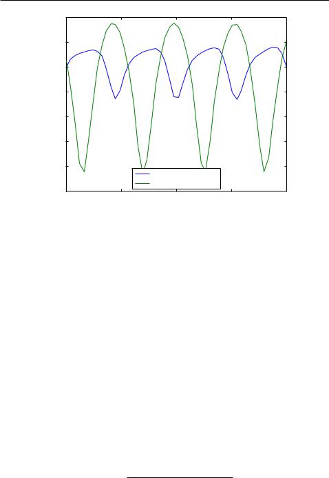
e ciency indicates the overlap between the exponential scattering mode from the grating and the Gaussian mode in an optical bre. The exponential scattering pattern can be engineered by varying the coupling strength of the grating coupler, and the maximized overlap was reported to be 80% [36], which is consistent with our simulation results shown in Fig. 4.4. The overall coupling e ciency (insertion loss) of the grating coupler can be expressed as the product of the two partial e ciency:
|
|
|
= 1 2 |
|
(4.5) |
|
|
−3 |
|
Directionality |
|
|
|
|
|
|
|
|
||
|
−4 |
|
Insertion loss |
|
|
|
|
−5 |
|
Reflction |
|
|
|
|
|
|
|
|
|
|
|
−6 |
|
|
|
|
|
(dB) |
−7 |
|
|
|
|
|
−8 |
|
|
|
|
|
|
power |
|
|
|
|
|
|
−9 |
|
|
|
|
|
|
|
|
|
|
|
|
|
|
−10 |
|
|
|
|
|
|
−11 |
|
|
|
|
|
|
−12 |
|
|
|
|
|
|
−13 |
1520 |
1540 |
1560 |
1580 |
1600 |
|
1500 |
|||||
|
|
|
wavelength (nm) |
|
|
|
Figure 4.4: Directionality, insertion loss and re ection to waveguide of a general fully-etched grating coupler
An optimal design can be found by optimizing the two partial e ciencies
1 and 2. The thickness of the buried oxide is determined by the wafer type, which is 2um in our case, 1 is xed with the given central wavelength and incident angle. The simulation results of a fully etched grating coupler with air cladding operated for TE mode at 1550nm have been shown in Fig. 4.4. The blue curve denotes the directionality of the grating, the green curve
61
4.1. Regular Fully Etched Grating Coupler
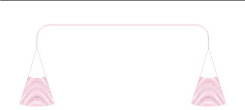
Figure 4.5: Mask layout of a fully etched grating coupler test structure
denotes the insertion loss of the grating, and the red curve denotes the back re ection to the waveguide of the grating. Due to the large refractive index contrast between the waveguide and the grating, the back re ection of the fully etched grating coupler is huge, which is even larger than the insertion loss of the grating coupler.
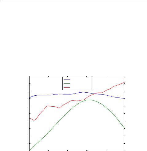
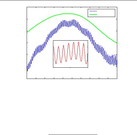
A mask layout of a fully etched grating coupler test structure is shown in Fig. 4.5. An input coupler and an output coupler are connected by a u-shape silicon wire waveguide. The centre-to-centre distance between the two grating couplers is 127 microns, which is determined by the pitch of thebre ribbon used in our lab. The comparison of simulation and measurement results for such a test structure is shown in Fig. 4.6. The green curve denotes the simulated insertion loss of the grating pair and the blue curve denotes the measured insertion loss of the same structure. Since the simulation result is obtained from the simulation of a single grating coupler, and the back re ection to the waveguide is not taken into consideration, no oscillations are shown in the simulation spectrum. Strong oscillations have been observed in the measurement spectrum of the grating structure, which is resulting from the large back re ection of the grating coupler. Such big ripples strongly a ect the performance of resonator structures such as ring resonators, disks, and Bragg gratings, etc.
62
4.1. Regular Fully Etched Grating Coupler
|
−10 |
|
|
|
|
|
|
|
|
|
|
|
|
|
|
|
|
|
|
|
Measurement |
|
|
|
|
|
|
|
|
|
|
|
Simulation |
|
|
|
−15 |
|
|
|
|
|
|
|
|
|
|
|
−20 |
|
|
|
|
|
|
|
|
|
|
(dB) |
−25 |
|
|
−15 |
|
|
|
|
|
|
|
power |
|
|
|
|
|
|
|
|
|
|
|
|
|
(dB) |
−16 |
|
|
|
|
|
|
|
|
|
|
−17 |
|
|
|
|
|
|
|
||
|
−30 |
|
power |
|
|
|
|
|
|
|
|
|
|
|
−18 |
|
|
|
|
|
|
|
|
|
|
|
|
|
|
|
|
|
|
|
|
|
−35 |
|
|
−19 |
|
1550 |
|
1555 |
|
|
|
|
|
|
|
1545 |
|
|
|
|
|
||
|
|
|
|
|
wavelength (um) |
|
|
|
|
||
|
−40 |
1510 |
1520 |
1530 |
1540 |
1550 |
1560 |
1570 |
1580 |
1590 |
1600 |
|
1500 |
||||||||||
wavelength (um)
Figure 4.6: Comparison of measurement result and simulation result of fullyetched grating coupler
The extinction ratio of the ripples shown in the measurement spectrum can be calculated by the transmission function of the Fabry-Perot cavity:
T = |
|
(1 R)2 |
|
(4.6) |
|
R)2 + 4 R sin2 |
|
||
(1 |
( =2) |
|||
where T denotes the transmitted power of a Fabry-Perot cavity, R is the re ectivity of the mirror, i.e., grating couplers in our case, and is the round trip phase shift. The re ectivity of the grating coupler is about 20% as shown in Fig. 4.4, so the extinction ratio of the ripples is about 2.8dB which is consistent with our measurement results shown in the inset of Fig. 4.6.
63
4.2.Improved Fully Etched Grating Coupler
4.2Improved Fully Etched Grating Coupler
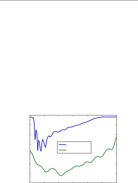
As we have discussed in the previous section, the bottlenecks faced by the fully etched grating couplers are the large back re ection to the waveguide and the high insertion loss. The strong back re ection of the fully etched grating couplers results from the large refractive index contrast between the waveguide and the grating. The simulation results of the back re ections of both shallow etched grating couplers and fully etched grating couplers are shown in Fig. 4.7. The green curve denotes the normalized back re ection of a shallow etched grating coupler designed based on a SOI with a 2-um buried oxide, 220 nm top Si layer, and air as the cladding. The blue curve denotes the back re ection of a fully etched grating coupler designed with the same wafer type and cladding. The grating couplers are designed for TE mode with a central wavelength of 1550 nm. The back re ection of the shallow etched grating coupler at the designed central wavelength is much smaller than that of the fully etched grating coupler and a di erence of more than 20 dB has been observed.
|
0 |
|
|
|
|
|
|
|
−5 |
|
|
|
|
|
|
|
−10 |
|
|
|
|
|
|
(dB) |
−15 |
|
|
full−etch |
|
|
|
power |
−20 |
|
|
shallow−etch |
|
|
|
|
|
|
|
|
|
||
|
|
|
|
|
|
|
|
|
−25 |
|
|
|
|
|
|
|
−30 |
|
|
|
|
|
|
|
−35 |
1450 |
1500 |
1550 |
1600 |
1650 |
1700 |
|
1400 |
||||||
|
|
|
wavelength (nm) |
|
|
||
Figure 4.7: Comparison of back re ections between shallow-etched grating coupler and fully-etched grating coupler
64

4.2. Improved Fully Etched Grating Coupler
Di erent approaches have been employed to tackle the issues of large back re ection and high insertion loss of fully etched grating couplers. Photonic crystal structures have been implemented in fully etched grating couplers to achieve low insertion loss [27]. However, customized wafers have been used to meet the requirement of the optimized design, which cannot be applied to the general cases with standard SOI wafers. Sub-wavelength structures [13, 14] have been used to reduce the back re ection and improve the insertion loss of the fully etched grating coupler at the same time. However, the reported designs are only applied for TM mode wave. In addition, all of the reported grating couplers are one-dimensional periodic structures and adiabatic tapers on the order of a few hundred micrometers are required to convert the optical mode from the grating to the waveguide, which waste a lot of precious space on the chip.
In this section, we will demonstrate a fully etched grating coupler for TE mode wave operated at 1550 nm with reduced back re ection and improved coupling e ciency. The proposed design is based on a SOI wafer with a 2um buried oxide and 220 nm top Si layer. The proposed design also has the potential to be converted to a compact structure with curved gratings, which has a much smaller footprint.
4.2.1Design Approach
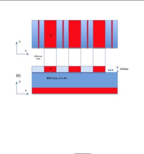
In order to reduce the back re ection of the fully etched grating couplers, we proposed a fully etched grating with e ective index areas consisting of air gaps and minor sub-wavelength gratings (show in Fig. 4.8). The major (wider) gratings determine the period and duty cycle of the grating coupler and the minor sub-wavelength gratings are employed to mitigate the refractive index contrast between the major gratings and the original air gaps. Those minor gratings are easier to be fabricated than the holes or rectangles [13, 14, 27]. Another advantage of the proposed design is the potential to be converted to compact structures with curved gratings. Based on the ideal mentioned in [6], one-dimensional gratings can be converted to more compact strcutures with curved gratings, which enables a much
65
4.2. Improved Fully Etched Grating Coupler
smaller footprint.
Figure 4.8: Schematic of a fully etched grating coupler with sub-wavelength gratings
According to the e ective medium theory (EMT), zeroth-order approximation can be applied to sub-wavelength structures with period-to-wavelength ratio, de ned as R = ne = , much smaller than 1:
1 |
= [ |
ff |
+ |
(1 ff) |
]1=2 |
(4.7) |
|
n(0) |
nL2 |
nsi2 |
|||||
|
|
|
|
||||
T E |
|
|
|
|
|
|
where n(0)TE denotes the refractive index of the approximated grating region, nL denotes the refractive index of the e ective index area with minor subwavelength gratings, nsi denotes the refractive index of the major grating, and ff is de ned as the ll factor of the grating. Second-order EMT can be used as a more accurate approximation to explore structures with lateral feature size of the same order as the wavelength in the medium [38]:
(2) |
(0) |
|
2 2 |
|
2 |
2 |
2 |
2 |
2 |
|
nT(0)M |
2 |
|
nT(0)E 4 |
|
1=2 |
|
|||
nT E |
= nT E |
[1 + |
|
|
R |
ff |
|
(1 ff) |
(nL nsi) |
|
( |
|
) |
( |
|
) |
] |
|
(4.8) |
|
|
3 |
|
|
ne |
nLnsi |
|
||||||||||||||
66