

Waves_in_Metamaterials
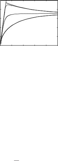
.pdfpropagation length [m]
3.3Surface plasmon–polaritons. Semi-infinite case, TM polarization 85
10−2
10−4
10−6 |
J /Z = 0.01 |
|
p p |
|
Jp/Zp= 0.1 |
|
free O |
10−8 |
OSPP |
10−6 |
10−5 |
|
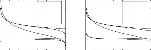
Fig. 3.7 Propagation length. fp = |
free space wavelength O[m] |
ωp/2π = 1200 THz |
|
3.3.3Penetration depth
The penetration depth into the dielectric, δd, or into the metal, δm, is the distance in the z direction from the surface over which the intensity of the field is reduced by a factor of e. It follows immediately that the penetration depth is inversely proportional to the imaginary part of the z component of the wave vector,
δd = |
1 |
, |
δm = |
1 |
. |
(3.23) |
||
|
|
|
|
|||||
2k |
|
2k |
|
|||||
|
z1 |
|
|
z1 |
|
|||
|
|
|
|
|
|
|||
In Section 1.10 we have already calculated the values of the normal components of the k vector in both media. The relationship is
kz1 = |
εr1μr1k02 − kx2 |
, kz2 = |
εr2μr2k02 − kx2 |
. |
(3.24) |
Disregarding losses we have seen already that the normal components are purely imaginary, which means that the field amplitudes decay away from the surface,
kz1 = −j κ1 , kz2 = −j κ2 . |
(3.25) |
A number of important conclusions may be drawn. case it may be shown that
δd |
|
εr2 |
. |
δm |
|
εr1 |
|
|
|
|
|
|
|
|
|
For the lossless
(3.26)
Since in the frequency range of surface plasmon–polaritons |εr2| ≥ εr1 (see eqns (3.10)), this means that the penetration depth in the surface active medium, metal, is always smaller than in the dielectric. At low frequencies, ω ωs, the penetration depth in the metal is much smaller than in the dielectric, whereas in the high-frequency limit with ω → ωs the penetration depths in the two media become comparable. Another
86 |
Plasmon–polaritons |
|
|
|
|
|
|||
|
|
10−4 |
|
|
|
|
δair |
|
|
|
|
|
|
|
|
δ |
|
|
|
|
|
|
|
|
|
|
metal |
|
|
|
|
|
|
|
|
|
skin depth |
|
|
|
[m] |
|
|
|
|
|
free space λ |
[m] |
|
|
|
|
|
|
|
λSPP |
|
||
|
penetration |
10−6 |
|
|
|
|
|
penetration |
|
|
|
|
|
|
|
|
|
||
|
|
|
|
|
|
|
|
|
|
|
|
10−8 |
|
|
|
|
|
|
|
|
|
0 |
0.1 |
0.2 |
0.3 |
0.4 |
0.5 |
0.6 |
0.7 |
|
|
|
|
|
|
ω/ωp |
|
|
|
|
|
|
|
|
|
(a) |
|
|
|
δair
10−4 |
δ |
|
metal |
skin depth free space λ
λSPP
10−6
10−8
0 |
0.1 |
0.2 |
0.3 |
0.4 |
0.5 |
0.6 |
0.7 |
ω/ωp
(b)
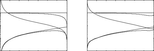
Fig. 3.8 Penetration depth for (a) γp = 0, (b) γp = 0.1ωp
interesting point is their very di erent asymptotic behaviour at low frequency,
δm |
λp |
, |
δd |
λ2 |
|
|
|
|
. |
(3.27) |
|||
4π |
4πλp |
|||||
The penetration depth in the metal in the low-frequency limit is practically frequency-independent, whereas the penetration depth in the dielectric is strongly frequency-dependent and can be quite large in the infra-red (Abeles, 1986).
Barnes et al. (2003) in their review pointed out the importance for the SPP-based nanocircuitry of these three characteristic length scales, the propagation length, the penetration depth into the dielectric and into the metal. The propagation length of the SPP mode, LSPP, is usually determined by the loss in the metal. For a low-loss metal, for example, silver, at a wavelength of 500 nm it is as large as 20 mm. The propagation length sets the upper size limit for any photonic circuit based on SPPs. The penetration depth into the dielectric material, δd, is typically of the order of one half the wavelength of light involved and dictates the maximum height of any individual features, and thus components, that might be used to control SPPs. The ratio of LSPP/δd thus gives one a measure of the number of SPP-based components that may be integrated together. The penetration depth into the metal, δm, determines the minimum feature size that can be used; this is between one and two orders of magnitude smaller than the wavelength involved, thus highlighting the need for good control of fabrication at the nanometer scale.
Another important point is that the penetration depth into the metal gives an idea of what thickness is required to allow coupling between the modes on the two surfaces of a thin metallic film. As shown later in Fig. 3.17(b) for a certain set of parameters, and as will be discussed in much
3.3Surface plasmon–polaritons. Semi-infinite case, TM polarization 87
|
101 |
|
|
|
|
|
|
|
|
101 |
|
|
|
|
|
|
|
|
100 |
|
|
|
|
|
free space λ |
|
100 |
|
|
|
|
|
free space λ |
||
δ/λ |
|
|
δair |
|
|
|
λSPP |
|
δ/λ |
|
|
δair |
|
|
|
λSPP |
|
penetration |
10−1 |
|
|
|
|
|
|
penetration |
10−1 |
|
|
|
|
|
|
||
|
|
|
skin depth |
|
|
|
|
|
skin depth |
|
|
||||||
|
|
|
|
|
|
|
|
|
|
|
|
||||||
|
|
|
|
|
|
δ |
|
|
|
|
|
|
|
δ |
|
||
|
|
|
|
|
|
metal |
|
|
|
|
|
|
|
metal |
|
||
|
|
|
|
|
|
|
|
|
|
|
|
|
|
|
|
||
|
10−2 |
|
|
|
|
|
|
|
|
10−2 |
|
|
|
|
|
|
|
|
10−3 |
0.1 |
0.2 |
0.3 |
0.4 |
0.5 |
0.6 |
0.7 |
|
10−3 |
0.1 |
0.2 |
0.3 |
0.4 |
0.5 |
0.6 |
0.7 |
|
0 |
|
0 |
||||||||||||||
|
|
|
|
|
ω/ωp |
|
|
|
|
|
|
|
|
ω/ωp |
|
|
|
|
|
|
|
|
(a) |
|
|
|
|
|
|
|
|
(b) |
|
|
|
|
|
Fig. 3.9 Penetration depth normalized to the free-space wavelength for (a) γp = 0, (b) γp = 0.1ωp |
|
||||||||||||||
more detail in Chapter 5, a film of 60 nm thickness at a wavelength around 360 nm may be regarded as too thick for an e ective coupling between the two surfaces. The subwavelength imaging mechanism relies on this coupling and therefore very thin films are essential there.
The penetration depth into the dielectric and into the metal are plotted in Figs. 3.8(a) and (b) as a function of ω/ωp for the lossless case, and for γp = 0.1ωp within the range of the SPPs from 0 to ωs. The free-space wavelength and the SPP wavelength are plotted as well for comparison. The penetration depth in the metal exhibits a remarkably constant value for a wide range of frequencies and there is not much di erence whether losses are present or not. There is though a di erence at very low frequencies where the penetration depth increases with decreasing frequency. At this stage it is interesting to compare the penetration depth with the skin depth (see, e.g., Solymar 1984), well known from undergraduate studies. Both the penetration depth and the skin depth stand for the same thing: how far the field will penetrate into the metal. The di erence between them is that the usual measure of the skin depth is for perpendicular incidence, implying a kx = 0, whereas kx is finite in the SPP case. As may be seen in Fig. 3.8, the deviation of the penetration depth from the skin depth is quite small. The curves of Fig. 3.8 are replotted in Fig. 3.9 but now normalized to the free-space wavelength.
The penetration depth into the dielectric is lower than λSPP at higher frequencies and larger than λSPP at lower frequencies. That increase, relative to the free-space wavelength, arises because at lower frequencies the metal is a better conductor and the dispersion of the SPP is closer to the light line and is less confined to the surface.
It is interesting to note that the penetration depth into the dielectric for a localized mode associated with nanoparticles can become much
88 Plasmon–polaritons
normalized eld at the boundary
1
0.8
0.6 |
|
E |
|
|
z1 |
|
|
Ez2 |
0.4 |
|
Ex |
0.2 |
|
|
0 |
10−5 |
10−4 |
10−6 |
free space wavelength O [m]
the boundary |
100 |
|
|
|
10−2 |
|
|
|
|
eld at |
|
|
|
|
normalized |
|
Ez1 |
|
|
−4 |
Ez2 |
|
|
|
10 |
Ex |
|
|
|
|
|
|
||
|
|
10−6 |
10−5 |
10 −4 |
free space wavelength O [m]
(a) |
(b) |
Fig. 3.10 Electric-field components at the metal–air interface
smaller, of the order of 10 nm (Whitney et al., 2005; Barnes, 2006). This is attributed to the divergence of the electric field around the tips of such structures. The larger the localization of the field near the metal surface, the larger is the field enhancement (Barnes, 1998). This enhanced field makes SPP modes sensitive to changes at the surface and opens up possibilities to use SPP modes for sensor applications (Barnes, 2006; Homola, 2003).
We can conclude from looking at Figs. 3.8 and 3.9 that as the freespace wavelength decreases both the propagation length and the penetration depth into the dielectric decrease. As ω approaches ωs, the wave penetrates to equal extents into both the dielectric and the metal, and as this happens the propagation length declines as well. So the correlation between confinement and attenuation may be roughly expressed as follows: the smaller the fraction of the wave in the metal, the smaller is the attenuation. We will return to this question when discussing the case of two interfaces.
3.3.4Field distributions in the lossless case
Next, we shall look at field distributions at the boundary. As seen before there is only one component of the magnetic field, Hy, along the y axis, while the electric field has two components, Ex and Ez in the sagittal plane that is defined by the normal to the surface (the z axis) and the direction of propagation (the x axis).
The field in the z direction is evanescent, reflecting the bound nonradiative nature of the SPP. No power is transferred in the normal direction away from the surface. The Hy and Ex components are continuous at the boundary, whereas the Ez component changes sign and can have a large discontinuity in its magnitude, depending on the ratio εr2/εr1.
normalized eld
1
0
−1
3.3 Surface plasmon–polaritons. Semi-infinite case, TM polarization 89
Ex
Ez
H y
−200 |
0 |
200 |
−100 |
0 |
100 |
−20 |
0 |
20 |
|
z [nm] |
|
|
z [nm] |
|
|
z [nm] |
|
|
(a) |
|
|
(b) |
|
|
(c) |
|
Fig. 3.11 Field amplitudes as a function of z for (a) ω/ωp = 0.25, (b) ω/ωp = 0.5, (c) ω/ωp = 0.7
The ratio of the transverse and longitudinal components of the electric field in the dielectric medium may be obtained from eqns (1.69) and (3.12) as
Ezx |
= j |
−εr1 |
= j |
|
|
|
|
|
(3.28) |
ε |
|
−ω2 . |
|||||||
|
|
|
|
|
ωp2 |
ω2 |
|
|
|
E 1 |
|
εr2 |
|
|
|||||
|
|
|
|
|
r1 |
|
|||
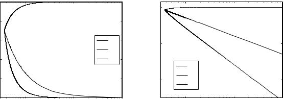
The transverse component is dominant in the electric field of SPPs with small wave numbers and low frequencies (light-like case) for which the dispersion curve is close to the dielectric light line. When kx k0 then the transverse and longitudinal components are comparable. They are equal when kx → ∞. The two components of the electric field at the boundary as a function of frequency, normalized to its maximum, are plotted in Fig. 3.10(a). They are replotted in Fig. 3.10(b) using a logarithmic scale in order to show how much smaller Ex is for most of the range.
The decay of the fields is faster in the metal than in the dielectric as follows from |κ2| being always larger than |κ1|. In Figs. 3.11(a)–(c) we
show the decay of Ez, |Ex| and Hy as a function of z in both media for
√
ω/ωp = 0.25, 0.5 and 0.7. It may be seen that as ω tends towards ωp/ 2 the decay in air becomes relatively stronger and the x and z components of the electric field become equal. The absolute decay strongly increases as ω increases, which may be seen by realizing that the scales in the three figures are di erent.
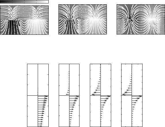
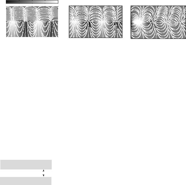
The amplitude of the magnetic field in the xz plane is shown in Figs. 3.12(a)–(c) by the gray-scale contrast for ω/ωp = 0.25, 0.5 and 0.7. The magnetic field may be seen to be more confined at ω/ωp = 0.7. Notice again the change of scale. The SPP wavelength is strongly reduced as ω approaches ωs. The electric field lines are also plotted in the same figure.
90 |
Plasmon–polaritons |
|
|
||
|
−1 |
−0.5 |
0 |
0.5 |
1 |
250 |
|
|
|
|
|
[nm] |
0 |
|
|
|
|
z |
|
|
|
|
|
−250 |
|
|
|
|
|
|
−500 |
−250 |
0 |
250 |
500 |
|
|
|
x [nm] |
|
|
(a)
100 |
|
|
|
|
20 |
|
|
|
|
[nm] 0 |
|
|
|
[nm] |
0 |
|
|
|
|
z |
|
|
|
z |
|
|
|
|
|
−100 |
|
|
|
−20 |
|
|
|
|
|
−200 |
−100 |
0 |
100 |
200 |
−40 |
−20 |
0 |
20 |
40 |
|
|
x [nm] |
|
|
|
|
x [nm] |
|
|
|
|
(b) |
|
|
|
|
(c) |
|
|
Fig. 3.12 Magnetic-field (contour plot) and electric-field (field lines) distribution at the metal–air boundary for (a) ω/ωp = 0.25,
(b) ω/ωp = 0.5, (c) ω/ωp = 0.7
z [nm]
200
100
0
−100
−200
z [nm]
x=0
(a)
80
40
0
−40
−80
x=0
(b)
|
30 |
|
20 |
|
20 |
|
15 |
|
|
|
|
|
|
|
10 |
|
10 |
|
5 |
|
|
|
|
z [nm] |
0 |
z [nm] |
0 |
|
|
||
|
−10 |
|
−5 |
|
|
|
|
|
|
|
−10 |
|
−20 |
|
−15 |
|
|
|
|
|
−30 |
|
−20 |
|
x=0 |
|
x=0 |
|
(c) |
|
(d) |
Fig. 3.13 Poynting vector in the vicinity of the metal–air interface for (a) ω/ωp = 0.25, (b) ω/ωp = 0.5, (c) ω/ωp = 0.685, (d) ω/ωp = 0.7. Lossless case
3.3.5Poynting vector: lossless and lossy
Knowing all field components we can easily calculate the magnitude and direction of the energy flow in the two media using the definition for the Poynting vector (Section 1.13). Without losses, there can be no Poynting vector component across the interface. Along the interface the x component of the Poynting vector may be written as
|
|
|
|
1 |
|
EzHy . |
|
|
|
||
|
|
|
|
Sx = − |
|
Re |
|
|
(3.29) |
||
|
|
|
|
2 |
|
|
|||||
With the aid of eqns (1.69) and (1.70) it takes the form |
|
|
|||||||||
Sx1 = |
kx |
|B|2 e |
2κ1z |
and |
Sx2 = |
kx |
|B|2 e |
−2κ2z , |
(3.30) |
||
2ωεr1 |
2ωεr2 |
||||||||||
3.3 Surface plasmon–polaritons. Semi-infinite case, TM polarization 91
z [nm]
200
100
0
−100
−200
z [nm]
x=0
(a)
|
|
30 |
|
20 |
|
80 |
|
|
|
15 |
|
|
|
20 |
|
||
|
|
|
|
||
40 |
|
|
|
10 |
|
|
10 |
|
|
||
|
|
|
5 |
||
|
[nm]z |
|
[nm]z |
||
0 |
0 |
0 |
|||
|
|
||||
|
|
−10 |
|
−5 |
|
−40 |
|
|
|
||
|
|
|
−10 |
||
|
|
|
|
||
|
|
−20 |
|
−15 |
|
−80 |
|
|
|
||
|
|
|
|
||
|
|
−30 |
|
−20 |
|
|
x=0 |
|
x=0 |
|
|
|
(b) |
|
(c) |
|
x=0 |
(d) |
Fig. 3.14 Poynting vector in the vicinity of the metal–air interface for (a) ω/ωp = 0.25, (b) ω/ωp = 0.5, (c) ω/ωp = 0.685, (d) ω/ωp = 0.7. Lossy case
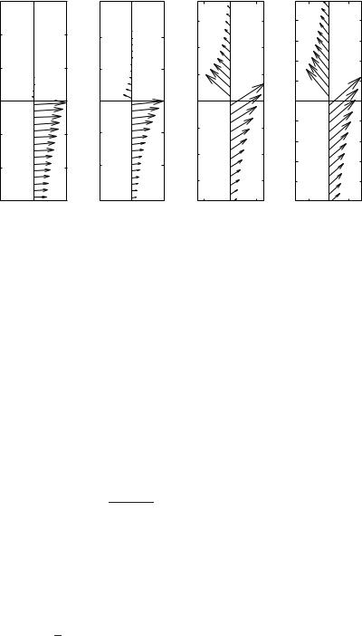
where Sx1 and Sx2 are the x components of the Poynting vector in the dielectric and in the metal, respectively. Taking εr1 = 1 the distribution of the Poynting vector is shown in Figs. 3.13(a)–(d) both in air and in the metal for ω/ωp = 0.25, 0.5, 0.685 and 0.7. It is interesting to note that practically all the power is flowing in air at ω/ωp = 0.25. The corresponding wave vector is close to the light line. As ω/ωp increases some of the power flows in the metal, oddly enough in the opposite direction. In the vicinity of the asymptote at ω/ωp = 0.7 the flow of power flowing in the positive and negative directions is nearly the same. There is very little net power flowing. If we want to find the net power of the SPP moving in the positive x direction we need to integrate Sx1 for z from −∞ to zero, and Sx2 from z = 0 to z = ∞. The integration can be easily performed. The final result after some algebra can be found as
Net power = B 2 |
kx |
|
εr22 − εr12 |
. |
(3.31) |
|
|
||||
| | |
4ωκ1 εr12 εr22 |
|
|||
When εr1 = |εr2| there is no net power flow at all. Otherwise, the net power is in the forward direction. We have a forward wave as follows anyway from the dispersion curve.
Why is there no Poynting vector component in the z direction? Both Ex and Hy are non-zero hence the normal component of the Poynting vector
|
1 |
ExHy |
|
Sz = |
2 Re |
(3.32) |
should exist. It does not for the reason that Ex and Hy are 90 degrees out of phase, and their product has zero real part.12 However, in the presence of losses (γp = 0.01ωp) Sz must be finite. The Poynting vector
12The same picture is known to occur in the case of total internal reflection.
92 |
Plasmon–polaritons |
|
|
|
|
|
|
|
|
|
|
|
|
||
|
−1 |
−0.5 |
0 |
0.5 |
1 |
|
|
|
|
|
|
|
|
|
|
500 |
|
|
|
200 |
|
|
|
|
40 |
|
|
|
|
||
[nm] |
0 |
|
|
|
[nm] |
0 |
|
|
|
[nm] |
0 |
|
|
|
|
z |
|
|
|
|
z |
|
|
|
|
z |
|
|
|
|
|
−500 |
|
|
|
−200 |
|
|
|
−40 |
|
|
|
|
|||
|
−1000 |
−500 |
0 |
500 |
1000 |
−400 |
−200 |
0 |
200 |
400 |
−80 |
−40 |
0 |
40 |
80 |
|
|
|
x [nm] |
|
|
||||||||||
|
|
|
|
|
|
|
x [nm] |
|
|
|
|
x [nm] |
|
|
|
(a) |
(b) |
(c) |
Fig. 3.15 Magnetic-field (contour plot) and electric-field (streamlines) distribution at the metal–air boundary. Lossy case
must cross the boundary between the dielectric and the metal in order to replenish the absorption occurring in the metal. This is shown in Figs. 3.14(a)–(d) for the same set of frequencies. An obvious consequence of losses is that the wave attenuates as it propagates in the x direction. Figures 3.15(a) and (b) show again (as in Fig. 3.12) the contour plots of Hy in the xz plane, and the field lines of the electric field. The strong decline of the magnetic field at ω = 0.7ωp may be clearly seen. There is a bright spot between x = −80 nm and −40 nm but one period away the intensity has so much declined that the maximum is hardly visible. Note also that the field lines, just as the streamlines of the Poynting vector, are slanted.
Dielectric
Metal |
|
d |
|
||
|
|
|
Dielectric
Fig. 3.16 Metallic slab surrounded by two identical semi-infinite dielectrics
3.4Surface plasmon–polaritons on a slab: TM polarization
So far we have had a single interface between two semi-infinite media. Now we consider a metallic slab of dielectric constant ε2 and thickness d in the z direction (see Fig. 3.16), and infinitely large in the other two directions. It is sandwiched between two homogeneous isotropic semiinfinite media of dielectric constant ε1. If the two surfaces are far away from each other then each one is unaware of the existence of the other one and no new phenomena occur. However, if the slab is su ciently thin then the SPP at one of the surfaces ‘feels’ the existence of the SPP at the other surface. A ‘repulsion of levels’ occurs, and the dispersion curves for the SPP localized at each of the two interfaces become split due to the interaction of these waves (Zayats et al., 2005).
3.4.1The dispersion equation
We have already considered the oblique incidence of a TM wave upon a slab in Section 1.11 and have already looked upon the transfer function with ‘perfect imaging’ in mind. Our interest now is to derive the disper-
3.4 Surface plasmon–polaritons on a slab: TM polarization 93
1 |
|
|
|
|
|
102 |
|
0.8 |
|
|
|
kpd=0.25 |
|
|
|
|
|
|
|
|
|
|
|
0.6 |
|
|
|
|
p |
|
1 |
p |
|
|
|
|
10 |
||
|
|
|
|
k |
|
||
ZZ/ |
|
|
kpd=0.5 |
|
/ |
|
|
|
|
|
x |
|
|
||
|
|
|
k |
|
|
||
0.4 |
|
|
|
|
|
|
|
|
|
kpd=1 |
|
|
|
|
|
0 2 |
|
|
|
|
|
|
|
|
|
|
|
|
|
100 |
|
0 |
2 |
4 |
6 |
8 |
10 |
|
|
0 |
|
|
|||||
|
|
|
kx /kp |
|
|
|
|
|
Hr=-1 |
|
|
|
|
Hr=-2 |
|
0 |
50 |
100 |
150 |
|
|
d [nm] |
|
(a) |
(b) |
Fig. 3.17 (a) Dispersion curves for thin slabs for kpd = 0.25, 0.5 and 1. (b) kx versus thickness for two di erent values of ω corresponding to εr = −1 and −2
sion equation. Like in the single-interface case we wish to find a solution with non-zero components Hy, Ex and Ez. The relationship between the input wave with amplitude A and the output wave with amplitude F is given by eqn (1.76). We have an eigensolution when there is an output without an input. This occurs when the denominator of eqn (1.76) is zero,13
(1 + ζe)2 − e −2κ2d(1 − ζe)2 = 0 , |
(3.33) |
where ζe = κ2ε1/(κ1ε2). The two solutions are |
|
(1 + ζe) = ±e −κ2d(1 − ζe) , |
(3.34) |
representing two modes guided by the metallic slab (in which the wave, now aware of both surfaces, travels with one single velocity), one symmetric and one antisymmetric with respect to their field distributions. As far as the dispersion curve is concerned it may be expected that the unperturbed dispersion curve (i.e. the one for the single interface) will split. The two branches of the dispersion equation given by eqn (3.34) can be expressed in more concise form as
ζe = −tanh |
κ2d |
, |
(3.35) |
|
2 |
|
|||
and |
|
|
|
|
ζe = −coth |
κ2d |
|
|
|
|
. |
(3.36) |
||
2 |
||||
These transcendental equations can be easily solved numerically. As shown above there are two solutions, first reported by Oliner and Tamir (1962). We shall denote the upper branch of the solution by ω(+) and
13The presence of a pole in expressions for field amplitudes is a typical feature of an eigenmode of a system. An alternative derivation, based on Maxwell’s equations, is given in Appendix G.
94 Plasmon–polaritons
Fig. 3.18 Electrostatic approximation and full solution for a slab. kpd = 0.25
|
1 |
|
|
|
|
|
|
0.8 |
|
|
|
|
|
p |
0.6 |
|
|
|
|
|
Z/Z |
0.4 |
|
|
|
|
|
|
|
|
|
|
|
|
|
0.2 |
|
|
|
|
|
|
00 |
2 |
4 |
6 |
8 |
10 |
|
|
|
|
kx/kp |
|
|
14It makes good sense that the surface modes that exist on a single interface at a given ω will split when the two surfaces are coupled. It is, however, less obvious that in the presence of coupling the so far prohibited territory between ωs and ωp may also be inhabited by a new mode, the upper branch of the dispersion curve. Physical considerations would suggest that such a mode is permissible because the basic condition εr2 < 0, is still valid, allowing charges to accumulate at the surface.
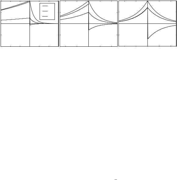
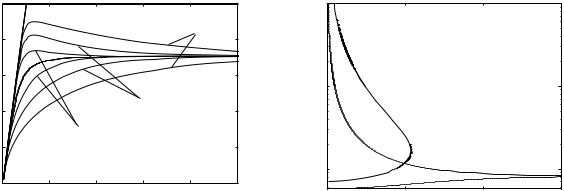
the lower branch by ω(−). In Fig. 3.17(a) we plot the upper and lower branches for εr1 = 1 and for three di erent thicknesses (kpd = 0.25, 0.5 and 1) together with the solution for the single interface (d → ∞) that is plotted with the dotted line. The meaning of the adjectives ‘upper’ and ‘lower’ make sense because they are above and below the dotted line. For large kx both curves tend towards ωs, the same limit as for the single interface. For small kx both types of dispersion curves tend to the light line. We also find, not unexpectedly, that the split between the modes becomes smaller as the slab becomes thicker. The propagation coe cient is plotted in Fig. 3.17(b) as a function of slab thickness for two di erent values of ω corresponding to εr = −1 and −2. It may be seen that for a large enough thickness only one mode may exist, or even none. The two surfaces are then uncoupled.14
It is always nice to find analytical approximations. They give a sense of security. We know what is going on. The first one presented is the electrostatic approximation that we have already come across in Section 2.12.4. It is described in Appendix F. For the present case we find the two branches of the dispersion equation in the form
|
ω2 |
|
ω2 |
= 2p 1 ± e −kxd . |
(3.37) |
For thin enough slabs the electrostatic approximation turns out to be extremely good for the lower branch, as may be seen in Fig. 3.18. It is good too for the upper branch until it reaches the light line but then it fails miserably. It cannot possibly follow the light line. This is of course not surprising. When the wave velocity is close to the velocity of light then nobody would expect an electrostatic approximation to work. Interestingly, the approximation for the lower branch is still quite good in the vicinity of the light line, although for su ciently low values of kx the approximation is bound to fail. How the approximation deteriorates for the lower branch as well as for low values of kx may be seen in Figs. 3.19(a)–(c) for three di erent thicknesses. The approximate curve is denoted by dashed lines. It may be seen that firstly the approximation crosses the light line and secondly that the approximation becomes worse as the thickness increases.