

2900
.pdfHow Probe works
Probe is another way to view simulation results. It lets you point to a location in a schematic and see the waveforms. It functions exactly like a normal simulation, saving all of the variables at each solution point in a disk file. When you click the mouse in the schematic, Probe determines where the mouse pointer is, extracts from the file the appropriate values for both the vertical and horizontal axes, and plots the resulting waveform. If you want, you can also enter expressions using circuit variables as you can in a standard analysis.
To illustrate Probe, load the file ECLGATE. Select Probe Transient from the Analysis menu. If a current analysis results file is not already available, the program runs a transient analysis on the circuit and saves the results in a file called ECLGATE.TSA. It then presents the Probe display. Click on the Probe menu. It provides these options:
•New Run: (F2) This option forces a new run. Probe automatically does a new run when the time of the last saved run is earlier than the time of the last edit to the schematic. However, if you have changed RELTOL or some other Global Settings value or option that can affect a simulation run, you may want to force a new run using the new value.
•Add Plot: This option lets you add a plot defined by a literal expression using any circuit variable. For example you might enter VCE(Q1)*IC(Q1) to plot a transistor's collector power.
•Delete Plots: This option lets you selectively remove waveforms.
•Delete All Plots: (CTRL + F9) This removes all waveforms.
•Separate Analog and Digital: This mode places the analog and digital waveforms in separate plot groups.
•One Trace: In this mode, only one waveform is plotted. Each time the schematic is probed, the old waveform is replaced with the new one.
38
•Many Traces: In this mode, new waveforms do not replace old ones, so many waveforms are plotted together, with common or individual vertical scales. The choice of common or individual scales is made by enabling or disabling the Same Y Scales option from the Scope menu.
•Save All: This option forces Probe to save all variables. Use it only if you need to display power, charge, flux, resistance, capacitance, inductance, В field, or H field.
•Save V and I Only: During a run, MC6 generates many variables. Saving them all to disk for display by Probe can create huge files. This option saves file space and lowers access time by saving only time, digital states, and voltage and current variables. It discards the remainder, including power, charge, flux, capacitance, inductance, resistance, and magnetic field values.
•Graph Group: This option lets you pick the plot group to place the next curve in. The next time you add an expression or click in the schematic to plot a curve it will be placed in the specified plot group. There are as many graphs as there are plot groups.
•Exit Probe (F3) : This exits Probe.
Transient analysis variables
The Vertical menu selects the vertical variable and the Horizontal menu selects the horizontal variable. Where the arrow tip of the mouse cursor touches the schematic, Probe determines whether the object is a node or a component and whether it is analog or digital.
If the object is a digital node, Probe plots the state waveform of the node.
If the object is analog, Probe extracts the vertical and horizontal variables specified by these menus and uses them to plot the analog curve or waveform. The analog variables available in transient analysis include:
39
•Voltage: If the mouse probes on a node, a node voltage is selected. If the mouse probes on the shape of a two-lead component, the voltage across the component is selected. If the mouse probes between two leads of a three or four lead active device, the lead-to-lead difference voltage is selected.
•Current: If the mouse probes on the shape of a two-lead component, the current through the component is selected. If the mouse probes on a lead of a three or four lead active device, the current into the lead is selected.
•Power: If the mouse probes on a component, it plots the power dissipated (PD), power generated (PG), or power stored (PS) in that component. If the component has more than one of these, a list appears allowing selection. In addition, the total circuit power generated PGT, the total circuit power dissipated PDT, and the total circuit power stored PST are available by clicking in any empty portion of the schematic.
•Resistance: If the mouse clicks on a resistor, this selects its resistance.
•Charge: If the mouse clicks on a capacitor, the capacitor's charge is selected. If the probe occurs between the leads of a semiconductor device, the charge of the internal capacitor between the two leads is selected. For example, a click between an NPN base and emitter selects the CBE charge.
•Capacitance: This is the capacitance associated with the charge.
•Flux: If the mouse clicks on the body of an inductor, this selects its flux.
•Inductance: This is the inductance associated with the flux.
•В Field: If the mouse clicks on a core, this selects the В field of the core.
•H Field: If the mouse clicks on a core, this selects the H field of the core.
•Time: This selects the transient analysis simulation time variable.
40
•Linear: This selects a linear plot.
•Log: This selects a log plot.
Probing node voltages
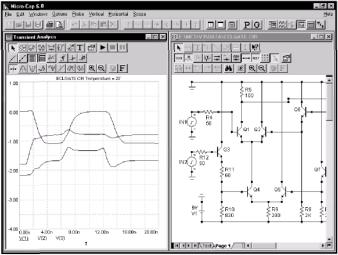
Click the Vertical menu and select Voltage. Select Time on the Horizontal menu. Click the left mouse button on the dot above the Ql collector lead. Probe scans the schematic, determines that the mouse is pointing to node 1, and plots V(l) vs. time. Probe on Ql's base lead dot, then probe on its emitter lead dot. The display should now look like this:
Figure 8-1 Probing node voltages
Probe uses a priority system to determine what it is looking at. It first checks to see if the location is within the shape outline of a component. If so and if the component is digital or a subckt or macro, Probe presents a list of pin names and lets you select one. If the part is anything else (e.g. a standard analog part), Probe tries to match the selected vertical and horizontal variables, like voltage or
41
current, with the variables available from the component. If there is a match, the variables are assigned and retrieved from the file. If there is no match, Probe checks to see if one of the selected variables is voltage and the location is on a non-ground node. If it is, it assigns the node's digital state or analog voltage to the variable and retrieves the values from the file.
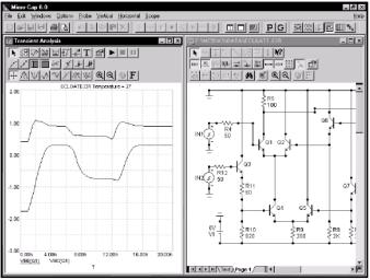
To illustrate plotting lead-to-lead voltages, press CTRL + F9 to remove all waveforms. Click the mouse midway between the Ql base lead dot and the Ql emitter lead. This plots one of the waveforms, VBE(Ql) or VEB(Ql), depending upon which lead the probe was closest to. It may take some practice to get the feel for where to probe. Add the VBC(Ql) waveform by clicking midway between the
Probing lead-to-lead voltages
The lead-to-lead voltage waveforms look like this:
Figure 8-2 Probing lead-to-lead voltages
42
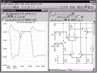
Lead currents can be plotted just as easily. Select Current from the Vertical menu. Press CTRL + F9 to remove all waveforms. Click on the base and emitter leads of Ql. The resulting waveforms show the current into each of these leads:
Figure 8-3 Probing lead currents
Navigating the schematic
Suppose you want to probe in an area of the schematic that is not visible? You can use any of the usual methods: scroll bars, mouse or keyboard panning, changing the scale, SHIFT + click relocation, or flag relocation.
To move around quickly use the SHIFT + click method. Press the SHIFT key and click the right mouse button anywhere in the circuit. The circuit shrinks. Move the mouse to another part of the circuit and press SHIFT + click. The scale reverts to normal and the view is centered at the mouse position.
Keyboard panning uses CTRL + any arrow key to move the view in the direction of the arrow. CTRL + PGUP and CTRL + PGDN move the
43
view up or down one page. The circuit window must be selected to pan the circuit view.
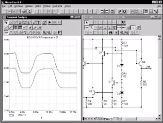
Mouse panning is the best way of navigating a localized area of the schematic. To illustrate, click in the Probe display and press CTRL + F9. Select Voltage from the Vertical menu. Click the left mouse button on Ql's collector dot to plot V(l) vs. time. Point the mouse near the middle of the circuit window, click the right mouse button, and hold it down. Drag the mouse to the left until the mouse is near the window border. Release the button and repeat the procedure until the Q8 transistor is in view. Click on the dot by the node labeled Out. The screen should look like this:
Figure 8-4 Waveforms from widely separated areas
An AC example
How about AC? The basic operation is the same, but there are differences. To illustrate the differences, press F3 to exit Probe and unload the ECLGATE circuit. Load the file DIFFAMP. Select Probe AC from the Analysis menu. Click on the Vertical menu. It looks like this:
44
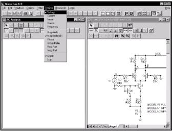
Figure 8-5 AC Probe variables and operators
The list of variables includes the usual voltage and current variables, but excludes charge, capacitance, flux, inductance, В, Н, and time. There are several new variables; INOISE, ONOISE, and frequency. Additionally, the complex math operators, Magnitude, Magnitude (dB), Phase (PH), Group Delay (GD), Real Part (RE), and Imag Part (IM) are available. The short form is shown in parentheses. One of these operators is always selected. When you choose a circuit variable by clicking in the schematic, the selected operator is applied to the circuit variable and the result plotted. Magnitude is the default operator. For example, V(10) is the magnitude of V(10). PH(V(10)) is the phase of V(10). As in normal AC analysis, the noise variables can not be mixed with other variables, such as voltage or current.
Click on the dot near the node labeled A. Using the right mouse button, pan the schematic to the left by dragging in the schematic. Pan until the right portion of the diffamp is visible. Click on the dot near
the node labeled OutA. Click on the Cursor mode button  to enable the Cursor mode. The results should look like Figure 8-6.
45
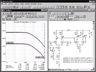
Figure 8-6 Reading AC gains using the Cursor mode
The left plot cursor is initially placed at the first data point, IKhz. The low frequency gain at the two nodes A and OutA can be read out directly under the Left column. Use the left mouse button to move the left cursor to obtain additional readings. The right plot cursor is controlled by the right mouse button.
Press CTRL + F9. Select Magnitude, Log, and ONOISE from the Vertical menu and click anywhere in the schematic. Select INOISE from the Vertical menu and click anywhere in the schematic. This plots input and output noise as shown at Fig. 8-7.
A DC example
We'll use the file DIFFAMP to illustrate the use of Probe in DC. Exit the AC Probe routine by pressing F3. Select Probe DC from the Analysis menu. Click on the Vertical menu. It looks like Fig. 8-8.
46
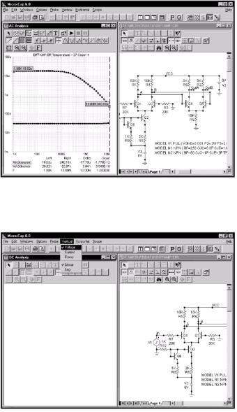
Figure 8-7 AC noise plots
Figure 8-8 DC Probe variables
47