

Учебное пособие 800637
.pdfPt
IrMn


GdFeCo


Pt
Ta
Glass
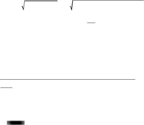
Figure. (a) Structure of the sample, (b) MFM profile of crater burned by femtosecond laser
The work was supported by Ministry of Education and Science of the Russian Federation (grant 3.1992.2017 /4.6). We are grateful to Prof. S.Mangin for fruitful discussions and samples presented in our disposal.
References
1.Hohlfeld J., Gerrits Th., Bilderbeek M., Rasing Th., Awano H., Ohta N. // Phys. Rev. B. – 2001. – V.65. – P.012413
2.Kato T., Nakazawa K., Komiya R., Nishizawa N., Tsunashima S., and Iwata De S.//Transactions on magnetic.- 2008.- V. 44.- P. 3380 - 3383.
537.9
,
|
|
|
|
|
|
Ё |
|
|
|
. . |
1, . . |
|
ё 2, . |
. |
3 . . |
4, . . |
5 |
|
|
|
1 |
- |
|
.- . |
, |
, kotovln@mail.ru |
|
|
|
|
|
|
2 |
. |
., mplasek@yandex.ru |
|
|
|
|
|
|
|
|
|
|
|
|||
|
3 |
. |
|
.- . |
, |
, uamkom@yandex.ru |
|
|
|
|
|
|
|
|
|||||
|
|
|
|
« |
. |
|
» |
|
|
|
4 |
- |
.- . |
, |
, kalinin48@mail.ru |
|
|
||
|
5 |
- |
.- . |
, |
, sitnikov04@mail.ru |
|
|||
|
« |
|
|
|
|
|
» |
|
|
(Co0.86+Nb0.12+Ta0.02)x+(SiO2)(1-x)/3. |
|
|
|
ё |
|
||||
|
|
|
|
. |
|||||
|
|
|
|
|
, |
|
|
ё |
|
|
|
- |
|
|
|
|
|
||
|
|
: |
|
|
ё . |
|
, |
ё |
, |
|
|
|
|
|
|
||||
, |
- |
|
|
, |
|
, |
|
. |
|
|
|
|
|
|
ё |
|
ё |
[1] |
- |
|
|
|
|
|
|
|
|
||
2- |
|
|
|
|
|
|
|
[2]. |
- |
|
ё |
|
|
|
|
|
|
. |
- |
|
|
|
|
|
|
|
|
||
|
|
|
|
. |
, |
|
|
|
- |
|
|
|
|
, |
. |
|
|
, |
- |
|
|
|
|
|
ё |
|
|
|
|
|
|
|
|
|
|
|
|
|
|
150
ё |
|
. |
|
, |
|
|
|
|
(Co0.86+Nb0.12+Ta0.02)x+(SiO2)(1-x)/3 ( |
|
|
||||
÷ 0.78) |
250 |
370 |
x ~ 0.14 |
||||
|
|
- |
|
|
|||
|
10-4 |
|
|
|
[3]. |
|
|
|
|
|
|
|
|
|
- |
. |
E6-17. |
|
|
ё |
|
|
- |
|
|
|
|
|
|
|
|
|
, |
|
|
|
GSP-7830, |
|
- |
|
|
12 |
3 |
50 |
1 |
, |
, |
|
|
ё |
[4]. |
|
|
||
|
|
|
|
|
|
||
|
|
|
ё |
. |
|
ё |
|
|
|
|
|
|
|
, |
- |
|
|
|
|
, |
|
|
- |
, |
|
|
. |
|
|
|
- |
|
|
|
x=0.78 |
|
|
|
|
x=0.62 |
|
|
. |
|
|
|
|
ё |
|
|
ё |
|
|
|
- |
, |
|
|
|
x=0.78 |
, |
|
ё |
x=0.62. |
|
|
|
|
|
|
- |
ё |
|
, |
|
|
( .1). |
|
|
|
x, |
|
|
|
, |
|
- |
|
|
|
|
|
|
|
- |
. |
x |
|
|
|
|
|
- |
. |
|
|
|
|
|
|
|
. |
|
|
|
|
|
ё |
x |
|
|
ё |
|
|
ё |
|
|
550 °C |
- |
|
|
|
|
|
|
, |
, |
|
|
|
|
|
|
|
. |
|
|
150001 ). |
|
|
|
|
( |
: №17–02–01138 , 17-57- |
||
|
|
|
|
|
|
|
|
|
1. |
, |
. . |
|
|
|
|
|
|
|
|
« |
- |
» |
|
|
/ . . |
|
[ |
.] // |
|
|
. – 2014. – N 4. – P.1-45. |
|
|
||
2. |
, . . |
|
|
|
|
|
|
|
1. – .26-37. |
– |
|
/ . . |
[ |
.] // |
. |
. 1. – 2009. – |
№ |
|
|
|
|
|
|
|
|
|
151
|
3. |
, |
. |
. |
|
- |
|
|
/ . . |
|
, . . |
, . . |
// |
|
|
. 2001. № 5. |
. 14–20. |
|
|
|
|
4. |
, . . |
|
, |
|
|
ё |
/ |
. . |
[ |
.] // |
. – 2015. – № 22 (377). – . 75-82. |
|
538.935, 538.975
|
. . |
1, |
|
|
1 |
|
|
2 |
3 |
. |
. |
|
4
«
10-4
,
77-300 K
350° .
200°
:
, |
, |
.
.
450°
,
,
.
[1].
. ,
-
sp2 –
. . |
2, |
. . |
3, . . |
4 |
|
|
|
, vlad_makagonov@mail.ru |
|
||
- |
|
, srgpank@mail.ru |
|
|
|
« |
|
|
|
» |
|
anton18885@yandex.ru |
|
|
|||
|
, vadim.foshin@yandex.ru |
» |
|
||
|
|
|
|
|
|
|
|
|
. |
, |
|
|
|
|
, |
|
|
|
, |
|
|
77 , |
|
|
. |
|
|
|
|
|
|
|
|
|
|
|
, |
|
, |
|
, |
|
|
|
, |
. |
|
|
~ 40 |
|
|
- |
|
|
|
|
|
~ 6·10-4 |
- |
|
|
-50, |
|
50° . |
- |
|
|
|
|
|
|
|
. |
|
|
, |
|
|
, |
|
|
|
|
|
|
|
10-4 |
|
|
|
|
10-4 |
. |
|
|
|
|
|
|
||
|
|
|
|
|
- |
|
|
|
. |
|
- |
|
|
|
77-300 K |
|
|
|
|
|
350° ( |
1 ), |
|
|
|
|
, |
, |
|
|
|
|
|
|
|
|
|
|
, |
225 ° |
|
|
|
|
|
- |
|
|
|
|
|
|
|
|
( |
1 ), |
|
- |
|
|
|
|
, |
, |
- |
|
|
|
|
|
|
|
|
|
[2], |
|
2D |
152
электроперенос в условиях слабой локализации электронов проводимости [3].
|
24 |
|
|
|
|
|
|
|
|
0,00 |
|
|
|
|
|
|
|
|
225 C |
|
|
22 |
|
|
|
|
|
|
|
% |
|
|
|
|
|
|
|
|
|
|
|
|
|
|
|
|
|
|
|
|
|
|
|
|
|
|
|
|
|
|
||
|
|
|
|
|
|
|
as deposited |
0,02 |
|
|
|
|
|
|
|
|
|
|
||
|
18 |
|
|
|
|
|
100, |
|
|
|
|
|
|
|
|
337 C |
||||
|
|
|
|
|
|
|
|
0,04 |
|
|
|
|
|
|
|
|
||||
|
20 |
|
|
|
|
|
|
|
|
|
|
|
|
|
|
|
|
|
||
m |
|
|
|
|
|
|
|
|
) |
0,08 |
|
|
|
|
|
|
|
|
450 C |
|
|
|
|
|
|
|
|
|
H |
|
|
|
|
|
|
|
|
||||
|
16 |
|
|
|
|
|
|
|
0 |
|
|
|
|
|
|
|
|
|
|
|
|
|
|
|
|
|
|
|
225 C |
/ |
0,06 |
|
|
|
|
|
|
|
|
|
|
|
14 |
|
|
|
|
|
|
337 C |
0 |
|
|
|
|
|
|
|
|
|
|
|
|
|
|
|
|
|
|
|
|
|
|
|
|
|
|
|
|
|
|
||
|
12 |
|
|
|
|
|
|
450 C |
- |
|
|
|
|
|
|
|
|
|
|
|
|
|
|
|
|
|
|
-( |
|
|
|
|
|
|
|
|
|
|
|
||
|
10 |
120 |
150 |
180 |
210 |
240 |
270 |
300 |
0,10 |
-8 |
-6 |
-4 |
-2 |
0 |
2 |
4 |
6 |
8 |
10 |
|
|
|
|||||||||||||||||||
|
90 |
|
-10 |
|||||||||||||||||
T, K |
H, kOe |
а) |
б) |
Рисунок. Зависимости удельного электросопротивления от температуры (а)
и магнитосопротивления (б) тонких пленок аморфного углерода в исходном состоянии и после термообработки при различных температурах
Таким образом, термообработка тонких пленок аморфного углерода, полученных методом ионно-лучевого распыления, приводит к смене механизма электропроводности от прыжков моттовского типа с переменной длиной прыжка [2] к слабой локализации и появлению квантовых поправок к проводимости [4].
Работа выполнена при поддержке грантов РФФИ № 19-48-360010 р_а.
Литература
1.Шкловский Б.И. Электронные свойства легированных полупроводников / Б.И. Шкловский, А.Л. Эфрос. – М.: Наука, 1979. – 416 с.
2.Калинин Ю.Е. Электрические свойства тонких пленок аморфного углерода, полученных методом ионно-лучевого напыления / Ю.Е. Калинин, М.А. Каширин, В.А. Макагонов, С.Ю. Панков, А.В. Ситников // Журнал технической физики. – 2017. – Т. 87. - Вып. 11. - С. 1722-1728.
3.Saleemi A.S. Structure dependent negative and positive magnetoresistance of amorphous carbon films / A.S. Saleemi, Sun W., Singh R., Luo Z., Zhang X. // Journal Of Applied Physics. 2017.
–Т. 121. – Вып. 23. - C. 233903.
4.Гантмахер, В.Ф. Электроны в неупорядоченных средах. 2–е изд. испр. и доп. / В.Ф.Гантмахер– М.: Физматлит, 2005. –232 с.
УДК 537.9
ИНТЕРПРЕТАЦИЯ ИЗМЕНЕНИЙ ПЛОТНОСТИ В ХОДЕ СТРУКТУРНОЙ РЕЛАКСАЦИИ И КРИСТАЛЛИЗАЦИ АМОРФНЫХ СПЛАВОВ
А.С. Макаров1, Ю.П. Митрофанов2, Р.А. Кончаков3, Н.П. Кобелев4, K. Csach5, J.C. Qiao6, В.А. Хоник7
1К-т физ.-мат. наук, доцент, a.s.makarov.vrn@gmail.com 2К-т физ.-мат. наук, доцент, ymitrofanov@vspu.ac.ru 3К-т физ.-мат. наук, доцент, konchakov@mail.ru 4К-т физ.-мат. наук, доцент, kobelev@issp.ac.ru 5Ph.D., csach@saske.sk
6Ph.D., qjczy@hotmail.com
7Д-р физ.-мат. наук, зав. кафедрой, v.a.khonik@vspu.ac.ru
1,2,3,7ФГБОУ ВО «Воронежский государственный педагогический университет» 4ФГБУН Институт физики твердого тела РАН, Черноголовка, РФ
5Institute of Experimental Physics SAS, Košice, Slovak Republic
6Northwestern Polytechnical University, Xi'an, China
В ходе анализа экспериментальных данных дилатометрических исследований и
измерений нерелаксированного модуля сдвига установлено, что изменения плотности,
153
. |
. |
|
|
|
|
|
|
: |
|
|
, |
, |
, |
|
|
|
|
|
|
||||
ё , |
. |
|
|
|
|
|
|
|
|
|
( |
) |
|
|
0,3– |
2% |
|
|
|
. |
|
|
- |
|
|
( |
). |
|
0,1–0,5% |
- |
|
|
|
|
|
[1]. |
|
|
- |
|
|
. |
|
, |
|
|
- |
|
|
|
|
|
. |
- |
|
|
|
|
|
|
|
||
|
|
|
|
. |
|
|
- |
|
[2] |
|
|
ё |
( |
|
- |
|
) |
[3]. |
|
|
|
|
- |
|
|
|
|
|
. |
|
- |
« |
ё |
» (free volume) « |
» (flow units) [4–5]. |
||||
, |
|
|
|
/ |
, |
|
- |
|
. |
|
|
|
|
|
|
|
|
|
|
|
|
- |
|
|
( |
) |
[6]. |
|
|
|
|
|
|
( |
) |
- |
|||
|
|
|
|
|
|||
. |
. |
|
|
|
|
, |
- |
|
|
|
- |
|
|
||
. |
|
|
|
|
|
|
- |
|
|
|
|
c |
|
- |
|
|
|
|
|
V / V (αi 1)c , |
|
||
|
|
|
ё |
V – |
|
ё , |
|
αi – |
ё |
|
|
. |
|
|
- |
c |
μ – |
|
|
G |
|
|
|
G μ exp( αg βc) , |
|
|
, αg 1 |
|
, |
- |
|
|
|
|
|
, β – |
|
. |
|
|
|
|
ё |
|
(1) |
|
|
|
|
|
|
|
|
|
|
(2):
|
|
|
ρ(t) |
|
αi |
1 |
|
|
G(t) |
, |
|
|
|||||
|
|
|
|
|
|
|
|
|
ln |
|
|
|
|||||
|
ρ |
|
|
β |
G0 |
(1) |
|
||||||||||
|
|
|
|
iso |
|
|
|
|
|
|
|
||||||
|
|
|
ρ(T ) |
|
|
|
|
|
μrt |
|
G(T ) |
|
|
|
|
||
|
|
|
|
αi 1 ln |
|
|
|
, |
|
|
|||||||
|
|
|
ρrt |
|
|
|
|
|
(2) |
|
|||||||
|
|
|
|
|
β |
|
Grt |
|
|
μ(T ) |
|
|
|||||
G0 |
G – |
|
( |
|
t 0 ) |
|
|
|
|
|
( |
|
|||||
t ) |
. |
|
|
«rt» |
|
|
|
|
|
|
|
|
|
|
- |
||
|
|
|
. |
|
|
|
|
|
|
|
|
|
|
|
|
- |
|
|
|
|
|
|
|
|
|
, |
|
|
|
|
|
|
(1) |
(2) |
- |
|
, |
|
|
|
|
|
|
|
|
|
|
|
|
|
, |
|
. |
|
|
, |
|
|
|
|
|
|
|
|
|
|
|
. |
|
||
|
|
|
|
|
|
|
|
|
|
|
|
|
|
|
|
||
|
|
|
|
|
|
|
|
|
|
|
|
|
|
|
|
№3.1310.2017/4.6. |
|
|
|
|
|
|
|
|
154 |
|
|
|
|
|
|
|
|
||
1.Wang W.H. The elastic properties, elastic models and elastic perspectives of metallic glasses / W.H. Wang // Prog. Mater. Sci. – 2012. - V. 57. - P. 487–656.
2.Egami T. Structural relaxation in amorphous alloys - compositional short range ordering / T. Egami // Mater. Res. Bull. – 1978. - V. 13. - P. 557–562.
3.Beukel A. On the kinetics of structural relaxation in metallic glasses / A. van den Beukel, S. Radelaar // Acta Metall. – 1983. - V. 31. - P. 419–427.
4.Xue R.J. Characterization of flow units in metallic glass through density variation / R.J. Xue, D.P. Wang, Z.G. Zhu, D.W. Ding, B. Zhang, W.H. Wang // J. Appl. Phys. – 2013. - V. 114. - P. 123514.
5.Gulzar A. Correlation between flow units and crystallization in metallic glasses / A. Gulzar, L.Z. Zhao, R.J. Xue, K. Shahzad, D.Q. Zhao, W.H. Wang // J. Non-Cryst. Sol. – 2017. - V. 461. - P. 61–66.
6.Granato A.V. Interstitialcy model for condensed matter states of face-centered-cubic metals / A.V. Granato // Phys. Rev. Lett. – 1992. - V. 68. - P. 974–977.
537.226.4
|
|
|
|
" |
|
|
- |
|
" |
|
|
|
. . |
|
|
1, . . |
|
2, . . |
3, . . |
4 |
|
|
|
1 |
. |
.- |
. |
, |
|
|
, dmakarev@rambler.ru |
|
|
||
|
|
|
|
|
|||||||
|
|
|
|
2 |
, lugovaya_maria@mail.ru |
|
|
|
|
||
|
|
|
|
|
|
|
|
|
|||
|
|
|
3 |
|
|
, reznichenkoan@yahoo.com |
|
|
|
||
|
|
|
|
|
|
|
|
|
|||
4 - |
|
.- |
. |
, |
|
|
, arybyanets@gmail.com |
|
|
||
|
|
|
|
« |
|
|
|
» |
|
|
|
|
|
|
" |
|
- |
" |
" |
|
- |
- |
", |
|
|
|
|
|
|
|
|
. |
|
. |
|
|
|
|
: |
|
|
, |
|
|
, |
|
|
|
|
|
|
|
|
|
|
|
|||
, |
|
|
, |
|
. |
|
|
|
|
|
|
|
|
|
|
|
|
|
[1]. |
|
|
|
- |
, |
|
|
|
3D |
|
|
|
|
|
|
- |
|
|
|
|
|
|
|
, |
. . |
|
. |
- |
|
. |
|
|
|
|
, |
|
|
|
|
- |
|
|
|
|
|
|
|
|
|
|
- |
|
. |
|
|
|
|
, |
|
|
|
: |
|
|
|
|
|
|
|
|
|
|
|
|||
|
|
|
|
|
, |
|
|
|
|
|
- |
, |
|
, |
|
|
, |
|
|
|
|
|
- |
|
, |
|
|
|
. |
|
|
, |
|
|
- |
|
|
|
|
|
|
|
|
|
|||
|
|
|
. |
|
|
|
|
|
|
|
- |
|
|
|
|
|
|
|
|
|
|
- |
|
|
|
|
|
|
|
|
|
|
|
|
|
|
|
|
, |
|
|
|
|
|
|
|
, |
|
|
. |
|
|
|
|
|
|
|
|
- |
|
|
|
|
|
|
155 |
|
|
|
|
|
|
|
|
-1 |
|
20 |
|
40%. |
|
|
|
- |
|
|
|
|
|
, |
|
|
|
|
|
- |
|
|
|
. |
|
|
|
|
|
|
. |
- |
[2]. |
|
|
|
|
|
|
|
|
|
|
- |
|
|
|
|
|
|
|
|
|
|
|
. |
|
, |
|
|
|
|
, |
|
|
|
|
- |
|
|
, |
|
|
|
|
|
|
|
, |
- |
|
[3]. |
|
|
, |
|
|
|
|
|
, |
- |
|
|
|
. |
|
, |
|
|
|
|
, |
, |
(9÷14) |
106 / |
2 . |
|
|
|
|
|
|
|
|
|
|
|
|
|
|
|
|
|
|
|||
|
|
|
|
|
|
|
|
|
|
|
- |
|
|
|
|
|
|
|
|
. |
|
, |
- |
|
|
|
, |
|
96%. |
|
|
235 |
, |
|
- |
|
|
|
|
|
|
|
|
|
|||
|
|
|
|
. |
|
|
|
|
|
|
- |
|
|
|
|
50 |
900 |
. |
|
5 |
|
, |
- |
|
|
|
|
|
|
|
|
|
|||
|
|
. |
, |
|
|
|
|
|
|
|
- |
|
|
|
|
|
|
|
|
|
( |
|
|
|
|
, |
№ 12.5425.2017/8.9) |
|
|
|
|
- |
|||
|
|
|
|
|
|
|
|||||
|
( |
№ 16-58-48009- |
- |
). |
|
|
|
|
|
|
|
|
1. |
|
. . |
|
|
|
|
|
|
/ . . |
|
|
. |
: |
, 2016. – 400 . |
|
|
|
|
|
|
|
|
|
2. |
. . |
|
|
|
|
|
|
|
" |
- |
- |
" |
|
0-3 / . . |
, |
. . |
|
, . . |
|
// |
|
|
. – 2005. |
. 31. - № 15. – . 80-84. |
|
|
|
|
|
|
|
|
||
|
3. |
. . |
− |
" / |
. . |
, |
. . |
, . |
. |
// |
- |
|
|
" |
|
||||||||
|
. – 2015. – .41. – |
. 7. – C. 22-27. |
|
|
|
|
|
|
|
||
UDC 537.9
INFLUENCE OF THERMAL TREATMENT ON STRUCTURE
AND ELECTRICAL PROPERTIES MULTILAYERED THIN FILMS BASED
ON OXIDE SEMICONDUCTORS
S.Yu. Pankov1, V.A. Makagonov2, O.V. Zhilova3, A.V. Sitnikov4, Yu.E. Kalinin5 1Ingeneer researcher, srgpank@mail.ru
2Cand. Phys.-Mat. of sciences, junior researcher, vlad_makagonov@mail.ru 3 Cand. Phys.-Mat. of sciences, junior researcher, zhilova105@mail.ru 4Dr. Phys.-Mat. sciences, professor, sitnikov04@mail.ru
5Dr. Phys.-Mat. sciences, professor, kalinin48@mail.ru Voronezh state technical university
Multilayered (In2O3/SnO2)69 thin films were obtained by ion-beam sputtering. XRD and TEM analysis showed that (In2O3/SnO2)69 samples are multilayered and In2O3 and SnO2 layers are
amorphous. The results showed that the multilayered samples were thermally stable up to the heat treatment temperature T <400°C. An increase in the temperature of heat treatment above 400°C
156
simultaneously leads to the crystallization of the amorphous phase for all values of the bilayer thickness and the destruction of the layered structure at bilayer thicknesses hbl > 2.5 nm.
Key words: multilayered heterostructures, oxide semiconductors, heat treatment, electrical resistivity, XRD.
At present time, multilayered heterostructures consisting of oxide semiconductors layers attract significant and growing interest for electronics devices application [1-3], gas sensors [4], etc. In most cases, such heterostructures exhibit improved or new physical properties and can combine the properties of two different materials. Multilayering is also a tool for regulating such structural parameters as the band gap width by influencing the structure of one layer on the structure of another [5,6].
In this paper, we presents results of research influence of thermal treatment on structure and electrical properties (In2O3/SnO2)69 multilayered heterostructures prepared by ionbeam sputtering. The structure of the samples was studied by X-ray diffraction methods
(XRD) on a Bruker D2 Phaser diffractometer ( CuKα1 = 1.54 |
|
). Heat treatment was provided |
in the vacuum chamber at the pressure is 10-2 Torr and in the temperature range 250- |
||
within 30 minutes. |
|
600 °C |
XRD analysis showed that (In2O3/SnO2)69 samples are multilayered and In2O3 and
SnO2 layers are amorphous (showed on figure). The results showed that the multilayered samples were thermally stable up to the heat treatment temperature T < 400 °C. An increase in the temperature of heat treatment above 400°C simultaneously leads to the crystallization
of the amorphous phase for all values of the bilayer thickness and the destruction of the layered structure at bilayer thicknesses hbl > 2.5 nm.
For samples with both small and large hbl, the conduction mechanism is thermally activated, in the temperature range close to room temperature. The results of the estimation of the activation energy correspond to the energy levels of oxygen vacancies in single-crystal SnO2.
(a) (b)
Figure. XRD patterns for (In2O3/SnO2)69 multilayered thin film sample (bilayer thickness hbl = 2,939 nm) (original and after annealing)
This work was supported by the Ministry of Education and Science of the Russian Federation as the project part of the state task (No 3.1867.2017/4.6).
References
1.Sanctis S. Stacked indium oxide/zinc oxide heterostructures as semiconductors in thin film
transistor devices: a case study using atomic layer deposition / S. Sanctis, J. Krausmann, C. Guhl // Journal of Materials Chemistry C. - 2018. – Vol. 6. – Issue. 3. - P. 464-472.
2.Lee S.J. High-Performance Amorphous Multi layered ZnO-SnO2 Heterostructure Thin-Film Transistors: Fabrication and Characteristics / Lee S.-J., Hwang C.-S., Pi J.-E., et.al. // Etri Journal. -
2015. – Vol. 37. – Issue. 6. - . 1135-1142.
3. Cui G., Han D., Dong J., et. al. Effects of channel structure consisting of ZnO /Al2O3 multilayers on thin-film transistors fabricated by atomic layer deposition / Cui G., Han D., Dong J., et. al. // Japanese Journal of Applied Physics. - 2017. – Vol. 56. – Issue. 4.– . 04CG03.
157
4. Mitu B. Multilayered metal oxide thin film gas sensors obtained by conventional and RF plasma-assisted laser ablation / Mitu B., Marotta V., Orlando S. // Applied Surface Science. - 2006. – Vol. 252. – Issue. 13. - . 4637-4641.
5. Bhattacharya P. Fabrication of stable wide-band-gap ZnO/MgO multilayer thin films / P. Bhattacharya, Rasmi R. Das, R. S. Katiyar // Appl. Phys. Lett. - 2003. – Vol. 83. - Issue. 10. - . 20102012.
6. Kaushal A. Pulsed laser deposition of transparent ZnO/MgO multilayers / A. Kaushal, D. Kaur // Journal of Alloys and Compounds. - 2011. – Vol. 509. – Issue. 2. - . 200-205.
UDC 537.9
INFLUENCE OF DISSIPATIVE PROPERTIES ON THE MAGNETOELECTRIC
COEFFICIENT IN MULTILAYER FILMS
V.N. Nechaev1, A.V. Shuba2
1Doct. of phys.-math. sci, Prof., wladnic@mail.ru 2Cand. of phys.-math. sci, Assoc. prof., shandvit@rambler.ru
Military Educational and Scientific Centre of the Air Force N.E. Zhukovsky
and Y.A. Gagarin Air Force Academy (Voronezh)
The dissipative properties of a two-layer ferromagnetic-piezoelectric system are taking into account to estimate the maximum value of the longitudinal coefficient of the magnetoelectric coupling Keywords: longitudinal magnetoelectric effect, dissipative properties of the ferromagnet-
piezoelectric system.
At the transition from a bulk sample to a film, as a result of the transition to another mathematical model — boundary problems for differential equations — the dependence of
the magnetoelectric (ME) coefficient αE on the geometric dimensions of the system is appear- ing. However, the restricted geometry consideration [1,2] can’t change the order of effect magnitude in resonance condition in the general case. If don’t consider the energy dissipation
processes in the structure, the response of the system will be abnormally large E . Let the two-layer structure of a ferromagnetic-piezoelectric be located in the x0y plane
perpendicular to the polarization P and magnetization M vectors. The equations of motion of the ferromagnetic (1) and piezoelectric (2) layers with lm and lp thicknesses have the form
|
|
|
1 |
2u 1 |
|
|
|
1 |
|
|
2u 1 |
|
1 |
3u 1 |
|
|
|
|
|
|||||||||
|
|
|
|
|
|
x |
G |
|
|
|
x |
|
|
|
|
|
x |
|
; |
|
|
|
(1) |
|||||
|
|
|
t 2 |
|
|
z2 |
|
|
t z 2 |
|
|
|
||||||||||||||||
|
|
|
|
|
|
|
|
|
|
|
|
|
|
|
|
|
|
|
|
|
|
|
|
|
|
|
|
|
|
|
2 |
2ux2 |
|
2 |
2ux2 |
G |
2 |
dzxz |
2 |
|
2 3ux2 |
, |
|||||||||||||||
|
|
|
t |
2 |
G |
|
|
|
|
z |
2 |
|
|
z |
2 |
t z |
2 |
|||||||||||
|
|
|
|
|
|
|
|
|
|
|
|
|
|
|
|
|
|
|
|
|
(2) |
|||||||
|
|
|
|
|
|
|
|
|
|
|
2 |
|
|
|
|
|
|
|
2u 2 |
|
|
|
||||||
zz |
|
|
|
|
|
2 |
|
|
|
|
|
|
|
2 |
|
|
|
|
||||||||||
4 dzxz2 |
G |
|
|
2 4 dzxzG |
|
|
x |
|
0. |
|
|
|||||||||||||||||
|
|
|
|
|
|
2 |
|
|
||||||||||||||||||||
|
|
|
|
|
|
|
|
|
|
|
z |
|
|
|
|
|
|
|
|
|
|
z |
|
|
|
|||
|
|
|
|
|
|
|
|
|
|
|
|
|
|
|
|
|
|
|
|
|
|
|
|
|||||
where j G j , j ,u j |
are the densities, shear modules, internal friction coefficients and |
|||||||||||||||||||||||||||
|
x |
|
|
|
|
|
|
|
|
|
|
ux j ,uz j for ferromagnetic (1) and piezoelec- |
||||||||||||||||
components of displacement vectors u j |
||||||||||||||||||||||||||||
tric (2) layers, respectively; φ is the electric potential of piezolayer; zz, dzxz are the components of the permittivity and piezoelectric modules tensors.
Solutions of equations (1), (2) will be found in the form
u j z,t g j z e i t , j 1, 2;
x (3)
z,t h z e i t ,
where ω is the frequency of external magnetic field oscillations, applied parallel to the P , M vectors. Substituting functions (3) into equations (1), (2), we obtain the equations for the amplitudes of the unknown functions:
158
|
|
2 g j |
|
2 |
j |
|
|
|
|
|
|
|||||||
|
|
|
|
|
|
|
|
|
|
|
g |
0, j 1, 2, |
(4) |
|||||
|
|
z |
2 |
|
|
j |
|
|
|
|||||||||
|
|
|
C |
|
|
|
|
|
|
|
|
|
|
|||||
|
|
|
|
|
|
|
|
|
|
|
|
|
|
|
|
|||
where C 1 |
G 1 i 1 |
/ 1 ,C 2 G |
2 |
zz |
/ |
|
zz |
4 d 2 |
|
G 2 |
i 2 |
/ 2 are rates propa- |
||||||
|
|
|
|
|
|
|
|
|
|
zxz |
|
|
|
|
||||
gation of elastic waves in the layers. Consideration the expression for the ME coefficient
E  Ez
Ez  ,
,
H0
where  Ez
Ez  is the average value of the electric field strength of the structure, and, linearizing
the denominator of the obtained expression for the coefficient of viscosity j , we get ME ratio for resonant frequencies ωi (i=0,1,2,3,…):
|
max |
|
8 dzxz |
2 C 1 C |
2 3 a |
|
|
E |
zzlp i2 cos ilm |
/ C 1 cos ilp / C 2 |
|||||
|
|
|
|||||
|
|
|
|
||||
(5)
2
2 C 2
|
ilpC |
|
/ C |
|
|
|
|
2 |
|
|
|
|
1 |
|
|||
|
1 |
2 |
|
|
|
1 |
|
|
|
||||||||
|
|
|
|
|
|
|
|
tg ilm / C |
|
|
|
|
|
|
|||
|
|
|
|
|
|
|
|
|
|
|
|
|
|
||||
2 |
ilp |
/ C |
2 |
|
|
|
1 |
C |
1 |
||||||||
cos |
|
|
|
|
|
|
|
|
|||||||||
|
|
|
|
|
|
|
|
|
|
|
|
|
|
|
|
|
|
|
|
|
|
|
|
C |
|
|
|
2 |
|
|
|
. |
|
|
2 |
|
1 |
|
|
|
|||||||
|
|
|
|
|
|
|
||||||||
|
ilmC |
|
|
/ |
|
|
|
|
2 |
|
|
|||
|
|
|
|
|
|
|
|
|
|
tg ilp / C |
|
|
|
|
2 |
ilm |
/ C |
1 |
|
|
|
||||||||
cos |
|
|
|
|
|
|
||||||||
|
|
|
|
|
|
|
|
|
|
|
|
|
|
|
The results, obtained by formula (5) for the nickel/PZT system, are shown in table.
Table The values of the ME coefficient Emax , V/ cm Oe at natural oscillations frequencies i , MHz ,
i 0, 3 of the composite at different thicknesses lp of the piezoelectric layer and thickness lm = 1 mm of the ferromagnetic layer
Piezolayer |
|
i=0 |
i=1 |
|
i=2 |
i=3 |
|
|
|||||
thickness |
ωi |
|
max |
ωi |
|
max |
ωi |
|
max |
ωi |
|
max |
|
lp, mm |
|
|
E |
|
|
E |
|
|
E |
|
|
E |
|
0.5 |
6.0621 |
|
4.418 |
12.1792 |
|
2.199 |
18.2384 |
|
1.468 |
24.3036 |
|
1.102 |
|
1.0 |
4.5440 |
|
125.533 |
9.0858 |
|
62.780 |
13.6319 |
|
41.844 |
18.1715 |
|
31.391 |
|
1.5 |
3.6346 |
|
18.610 |
7.2413 |
|
9.341 |
10.8919 |
|
6.210 |
14.5011 |
|
4.664 |
|
It should be noted that the evaluation method max |
in the papers [1,2] is not clear, |
||||||||||||
|
|
|
|
|
|
|
E |
|
|
|
|
|
|
since the parameters of the dissipative materials are absent in the corresponding formulas.
References
1.Bichurin M.I., Filippov D.A., Petrov V.M., Laletsin V.M., Paddubnaya N., Srinivasan G. // Phys. Rev. B. 2003. V. 68. P.132408.
2.Bichurin M.I., Petrov V.M., Averkin S.V., and Filippov A.V. // Phys. Solid State. 2010. V.
52.10. P. 2116.
:537.9
Ni-(AlZrO)
. . |
|
1, |
. . |
2, . |
3, . . |
4 |
1 |
|
|
, kristina_yakovleva_555@mail.ru |
|
||
|
|
|
|
|
|
|
|
|
2 |
|
, deadpank@mail.ru |
|
|
|
|
|
|
|
||
|
3 |
|
|
, Hemzaadili0@gmail.com |
|
|
|
|
|
|
|
||
4 |
- |
.- |
. |
, |
, sto@sci.vrn.ru |
|
« |
|
|
|
|
|
» |
159