

MAX44242
Typical Application Circuit
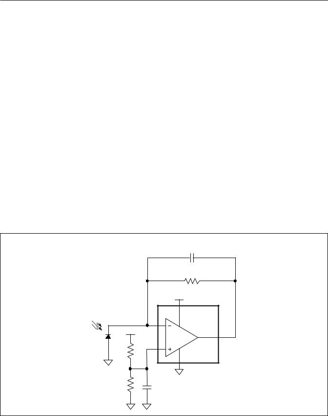
High-Impedance Sensor Application
High impedance sources like pH sensor, photodiodes in applications require negligible input leakage currents to the input transimpedance/buffer structure. The MAX44242 benefits with clean and precise signal conditioning due to its input structure.
The device interfaces to both current-output sensors (photodiodes) (Figure 1), and high-impedance voltage sources (piezoelectric sensors). For current output sensors, a transimpedance amplifier is the most noise-effi- cient method for converting the input signal to a voltage. High-value feedback resistors are commonly chosen to create large gains, while feedback capacitors help stabilize the amplifier by cancelling any poles introduced in the feedback loop by the highly capacitive sensor or cabling. A combination of low-current noise and low-voltage noise is important for these applications. Take care to calibrate out photodiode dark current if DC accuracy is important. The high bandwidth and slew rate also allow AC signal processing in certain medical photodiode sensor applications such as pulse-oximetry. For voltage-output sensors, a noninverting amplifier is typically used to buffer and/or
20V, Low Input Bias-Current,
Low-Noise, Dual Op Amplifier
apply a small gain to the input voltage signal. Due to the extremely high impedance of the sensor output, a low input bias current with minimal temperature variation is very important for these applications.
Transimpedance Amplifier
As shown in Figure 2, the noninverting pin is biased at 2V with C2 added to bypass high-frequency noise. This bias voltage to reverse biases the photodiode D1 at 2V which is often enough to minimize the capacitance across the junction. Hence, the reverse current (IR) produced by the photodiode as light photons are incident on it, a proportional voltage is produced at the output of the amplifier by the given relation:
VOUT = IR × R1
The addition of C1 is to compensate for the instability caused due to the additional capacitance at the input (junction capacitance Cj and input capacitance of the op amp CIN), which results in loss of phase margin. More information about stabilizing the transimpedance amplifier can be found in Application Note 5129: Stabilize Your Transimpedance Amplifier.
|
C1 |
|
15nF |
|
R1 |
|
100kΩ |
|
+5V |
|
MAX44242 |
5V |
D1 |
|
R2
30kΩ
R3 |
C2 |
20kΩ |
10nF |
Figure 1. High-Impedance Source/Sensor Preamp Application
www.maximintegrated.com |
Maxim Integrated │ 9 |