

бакМИТ_КП2015 / Компоненты по вариантам / Операционные_усилители / MAX9910EXK
.pdf19-3406; Rev 2; 10/10
200kHz, 4µA, Rail-to-Rail I/O Op Amps with Shutdown
General Description
The single MAX9910/MAX9911 and dual MAX9912/ MAX9913 operational amplifiers (op amps) feature a maximized ratio of gain bandwidth (GBW) to supply current and are ideal for battery-powered applications such as portable instrumentation, portable medical equipment, and wireless handsets. These CMOS op amps feature an ultra-low input-bias current of 1pA, rail- to-rail inputs and outputs, low supply current of 4µA, and operate from a single 1.8V to 5.5V supply. For additional power conservation, the MAX9911/MAX9913 feature a low-power shutdown mode that reduces supply current to 1nA, and puts the amplifiers’ outputs in a high-impedance state. These devices are unity-gain stable with a 200kHz GBW product.
The MAX9910 is available in a 5-pin SC70 package. The MAX9911 is available in tiny 6-bump WLP and a 6-pin SC70 packages. The MAX9912 is available in an 8-pin SOT23 package, and the MAX9913 is available in a 10pin µMAX® package. All devices are specified over the -40°C to +85°C extended operating temperature range.
Applications
Portable Medical Devices
Portable Test Equipment
Laptops
Data-Acquisition Equipment
Typical Operating Circuit
|
|
1.8V TO 5.5V |
|
OUTA |
|
VDD |
|
|
|
|
|
INA- |
|
OUTB |
VOUT |
|
|
|
25kΩ |
INA+ |
|
INB- |
|
VMID |
|
|
|
VSS |
|
INB+ |
VMID + VBIAS |
|
|
||
MAX9913 |
|
|
|
ON |
|
|
ON |
SHDNA |
|
SHDNB |
|
OFF |
|
|
OFF |
1MΩ |
RE |
|
|
|
|
|
|
CE |
GLUCOSE |
WE |
|
SENSOR |
|
||
THREE ELECTRODE GLUCOSE METER APPLICATION WITH SHUTDOWN |
|
||
Features
♦200kHz GBW
♦Ultra-Low 4µA Supply Current
♦Single 1.8V to 5.5V Supply Voltage Range
♦Ultra-Low 1pA Input Bias Current
♦Rail-to-Rail Input and Output Voltage Ranges
♦Low ±200µV Input Offset Voltage
♦Low 0.001µA Shutdown Current
♦High-Impedance Output During Shutdown (MAX9911/MAX9913)
♦Unity-Gain Stable
♦Available in Tiny WLP, SC70, SOT23, and µMAX Packages
Ordering Information
PART |
TEMP RANGE |
PIN- |
TOP |
|
PACKAGE |
MARK |
|||
|
|
|||
|
|
|
|
|
MAX9910EXK+T |
-40°C to +85°C |
5 SC70 |
AGA |
|
MAX9910EXK-T |
-40°C to +85°C |
5 SC70 |
AGA |
|
|
|
|
|
|
MAX9911EXT+T |
-40°C to +85°C |
6 SC70 |
ACA |
|
|
|
|
|
|
MAX9911EXT-T |
-40°C to +85°C |
6 SC70 |
ACA |
|
|
|
|
|
|
MAX9911EWT+ |
-40°C to +85°C |
6 WLP |
BQ |
|
|
|
|
|
|
MAX9912EKA+T |
-40°C to +85°C |
8 SOT23 |
AEJY |
|
|
|
|
|
|
MAX9912EKA-T |
-40°C to +85°C |
8 SOT23 |
AEJY |
|
|
|
|
|
|
MAX9913EUB |
-40°C to +85°C |
10 µMAX |
— |
|
|
|
|
|
|
MAX9913EUB+ |
-40°C to +85°C |
10 µMAX |
— |
|
|
|
|
|
+Denotes lead(Pb)-free/RoHS-compliant package.
Selector Guide
PART |
AMPLIFIERS |
SHUTDOWN |
|
PER PACKAGE |
MODE |
||
|
|||
|
|
|
|
MAX9910EXK-T |
1 |
No |
|
|
|
|
|
MAX9911EXT-T |
1 |
Yes |
|
|
|
|
|
MAX9912EKA-T |
2 |
No |
|
|
|
|
|
MAX9913EUB |
2 |
Yes |
µMAX is a registered trademark of Maxim Integrated Products, Inc.
________________________________________________________________ Maxim Integrated Products 1
MAX9913–MAX9910
For pricing, delivery, and ordering information, please contact Maxim Direct at 1-888-629-4642, or visit Maxim’s website at www.mxim-ic.com.

MAX9910–MAX9913
200kHz, 4µA, Rail-to-Rail I/O Op Amps with Shutdown
ABSOLUTE MAXIMUM RATINGS
Power-Supply Voltage (VDD to VSS) |
...................... |
-0.3V to +6.0V |
8-Pin SOT23 (derate 9.1mW/°C above +70°C)........... |
727mW |
||
IN_+, IN_-, OUT_, SHDN_............... |
(V SS - 0.3V) to (VDD + 0.3V) |
10-Pin µMAX (derate 5.6mW/°C above +70°C) ........... |
444mW |
|||
Current into IN_+, IN_- ...................................................... |
|
|
±20mA |
Operating Temperature Range .......................... |
-40°C to +85°C |
|
Output Short-Circuit Duration to VDD ..............or VSS |
|
Continuous |
Junction Temperature ..................................................... |
|
+150°C |
|
Continuous Power Dissipation (TA = +70°C) |
|
|
Storage Temperature Range ............................ |
-65°C to +150°C |
||
5-Pin SC70 (derate 3.1mW/°C above .............+70°C) |
|
247mW |
Lead Temperature (excluding WLP, soldering 10s) ........ |
+300°C |
||
6-Bump WLP (derate 10.5mW/°C above +70°C) |
.........840mW |
Soldering Temperature (reflow) |
|
|
||
6-Pin SC70 (derate 3.1mW/°C above .............+70°C) |
|
245mW |
Lead(Pb)-Free Packages............................................. |
|
+260°C |
|
|
|
|
|
Packages Containing Lead(Pb)................................... |
|
+240°C |
Stresses beyond those listed under “Absolute Maximum Ratings” may cause permanent damage to the device. These are stress ratings only, and functional operation of the device at these or any other conditions beyond those indicated in the operational sections of the specifications is not implied. Exposure to absolute maximum rating conditions for extended periods may affect device reliability.
ELECTRICAL CHARACTERISTICS
(VDD = 1.8V to 5.5V, VSS = 0V, VCM = 0V, VOUT = VDD / 2, RL = ∞ connected to VDD / 2, SHDN_ = VDD, TA = +25°C, unless otherwise noted.) (Note 1)
PARAMETER |
SYMBOL |
CONDITIONS |
MIN |
TYP |
MAX |
UNITS |
|
Supply Voltage Range |
VDD |
Guaranteed by PSRR test |
1.8 |
|
5.5 |
V |
|
|
|
MAX9910/MAX9911 |
VDD = 1.8V |
|
4 |
|
|
Supply Current |
IDD |
VDD = 5.5V |
|
4 |
5.0 |
µA |
|
|
|
||||||
MAX9912/MAX9913 |
VDD = 1.8V |
|
7 |
|
|||
|
|
|
|
|
|||
|
|
VDD = 5.5V |
|
7 |
9 |
|
|
|
|
|
|
|
|||
Shutdown Supply Current |
IDD(SHDN_) |
SHDN_ = GND, MAX9911/MAX9913 |
|
0.001 |
0.5 |
µA |
|
Input Offset Voltage |
VOS |
|
|
|
±0.2 |
±1 |
mV |
Input-Offset-Voltage Matching |
|
MAX9912/MAX9913 |
|
|
±250 |
|
µV |
Input Bias Current |
IB |
(Note 2) |
|
|
±1 |
±10 |
pA |
Input Offset Current |
IOS |
(Note 2) |
|
|
±1 |
±10 |
pA |
Input Resistance |
RIN |
Common mode |
|
|
1 |
|
GΩ |
|
|
|
|
|
|||
Differential mode, -1mV < VIN < +1mV |
|
10 |
|
||||
|
|
|
|
|
|||
Input Common-Mode Range |
VCM |
Guaranteed by CMRR test |
VSS - |
|
VDD + |
V |
|
0.1 |
|
0.1 |
|||||
|
|
|
|
|
|
||
|
|
|
|
|
|
|
|
Common-Mode Rejection Ratio |
CMRR |
-0.1V < VCM < VDD + 0.1V, VDD = 5.5V |
70 |
80 |
|
dB |
|
Power-Supply Rejection Ratio |
PSRR |
1.8V < VDD < 5.5V |
|
65 |
95 |
|
dB |
|
|
25mV < VOUT < VDD - 25mV, |
95 |
120 |
|
|
|
|
|
RL = 100kΩ, VDD = 5.5V |
|
|
|||
Open-Loop Gain |
AVOL |
|
|
|
dB |
||
100mV < VOUT < VDD - 100mV, |
95 |
110 |
|
||||
|
|
|
|
||||
|
|
RL = 5kΩ, VDD = 5.5V |
|
|
|
||
|
|
|
|
|
|
|
|
|
|
|
RL = 100kΩ |
|
2.5 |
5 |
|
Output-Voltage-Swing High |
VOH |
VDD - VOUT |
RL = 5kΩ |
|
50 |
70 |
mV |
|
|
|
RL = 1kΩ |
|
250 |
|
|
|
|
|
RL = 100kΩ |
|
2.5 |
5 |
|
Output-Voltage-Swing Low |
VOL |
VOUT - VSS |
RL = 5kΩ |
|
50 |
70 |
mV |
|
|
|
RL = 1kΩ |
|
250 |
|
|
Channel-to-Channel Isolation |
CHISO |
Specified at DC, MAX9912/MAX9913 |
|
100 |
|
dB |
|
Output Short-Circuit Current |
IOUT(SC) |
|
|
|
±15 |
|
mA |
2_______________________________________________________________________________________

200kHz, 4µA, Rail-to-Rail I/O Op Amps with Shutdown
ELECTRICAL CHARACTERISTICS (continued)
(VDD = 1.8V to 5.5V, VSS = 0V, VCM = 0V, VOUT = VDD / 2, RL = ∞ connected to VDD / 2, SHDN_ = VDD, TA = +25°C, unless otherwise noted.) (Note 1)
PARAMETER |
SYMBOL |
|
CONDITIONS |
MIN |
TYP |
MAX |
UNITS |
||
|
|
|
|
|
|
|
|
|
|
SHDN_ Logic Low |
VIL |
VDD = 1.8V to 3.6V, MAX9911/MAX9913 |
|
|
0.4 |
V |
|||
VDD = 3.6V to 5.5V, MAX9911/MAX9913 |
|
|
0.8 |
||||||
|
|
|
|
|
|
||||
SHDN_ Logic High |
VIH |
VDD = 1.8V to 3.6V, MAX9911/MAX9913 |
1.4 |
|
|
V |
|||
VDD = 3.6V to 5.5V, MAX9911/MAX9913 |
2 |
|
|
||||||
|
|
|
|
|
|
||||
SHDN_ Input Bias Current |
IIL |
SHDN_ = VSS, MAX9911/MAX9913 (Note 2) |
|
|
1 |
nA |
|||
IIH |
SHDN_ = VDD , MAX9911/MAX9913 |
|
|
500 |
|||||
|
|
|
|
||||||
Output Leakage in Shutdown |
IOUT(SHDN_) |
SHDN_ = VSS, VOUT = 0V to VDD, |
|
1 |
500 |
nA |
|||
MAX9911/MAX9913 |
|
||||||||
|
|
|
|
|
|
|
|
|
|
Gain-Bandwidth Product |
|
|
|
|
|
|
200 |
|
kHz |
|
|
|
|
|
|
|
|
|
|
Slew Rate |
|
|
|
|
|
|
0.1 |
|
V/µs |
|
|
|
|
|
|
|
|
|
|
Capacitive-Load Stability (See |
|
|
|
|
AV = 1V/V |
|
30 |
|
|
|
|
No sustained |
|
AV = 10V/V |
|
250 |
|
|
|
the Driving Capacitive Loads |
CLOAD |
|
|
|
|
pF |
|||
|
oscillations |
|
RL = 5kΩ, AV = 1V/V |
|
200 |
|
|||
Section) |
|
|
|
|
|
|
|||
|
|
|
|
RISO = 1kΩ, AV = 1V/V |
|
100 |
|
|
|
|
|
|
|
|
|
|
|
||
Input Voltage-Noise Density |
|
|
f = 1kHz |
|
|
|
400 |
|
nV/√Hz |
Input Current-Noise Density |
|
|
f = 1kHz |
|
|
|
0.001 |
|
pA/√Hz |
Settling Time |
|
|
To 0.1%, VOUT = 2V step, AV = -1V/V |
|
18 |
|
µs |
||
Delay Time to Shutdown |
tSH |
IDD = 5% of normal operation, |
|
2 |
|
µs |
|||
VDD = 5.5V, VSHDN_ = 5.5V to 0 step |
|
|
|||||||
|
|
|
|
|
|
|
|||
Delay Time to Enable |
tEN |
VOUT = 2.7V, VOUT settles to 0.1%, |
|
30 |
|
µs |
|||
VDD = 5.5V, VSHDN_ = 0 to 5.5V step |
|
|
|||||||
|
|
|
|
|
|
|
|||
Power-Up Time |
|
|
VDD = 0 to 5.5V step |
|
5 |
|
µs |
||
MAX9913–MAX9910
ELECTRICAL CHARACTERISTICS
(VDD = 1.8V to 5.5V, VSS = 0V, VCM = 0V, VOUT = VDD / 2, RL = ∞ connected to VDD / 2, SHDN_ = VDD, TA = -40°C to +85°C, unless otherwise noted.) (Note 1)
PARAMETER |
SYMBOL |
CONDITIONS |
MIN |
TYP |
MAX |
UNITS |
|
|
|
|
|
|
|
|
|
Supply Voltage Range |
VDD |
Guaranteed by PSRR test |
1.8 |
|
5.5 |
V |
|
Supply Current |
IDD |
MAX9910/MAX9911 |
VDD = 5.5V |
|
|
5.5 |
µA |
|
|
|
|
||||
MAX9912/MAX9913 |
|
|
11 |
||||
|
|
|
|
|
|
||
Shutdown Supply Current |
IDD(SHDN_) |
SHDN_ = GND, MAX9911/MAX9913 |
|
|
1 |
µA |
|
Input Offset Voltage |
VOS |
|
|
|
|
±5 |
mV |
Input-Offset-Voltage |
TCVOS |
|
|
|
±5 |
|
µV/°C |
Temperature Coefficient |
|
|
|
|
|||
|
|
|
|
|
|
|
|
|
|
|
|
|
|
|
|
_______________________________________________________________________________________ 3

MAX9910–MAX9913
200kHz, 4µA, Rail-to-Rail I/O Op Amps with Shutdown
ELECTRICAL CHARACTERISTICS (continued)
(VDD = 1.8V to 5.5V, VSS = 0V, VCM = 0V, VOUT = VDD / 2, RL = ∞ connected to VDD / 2, SHDN_ = VDD, TA = -40°C to +85°C, unless otherwise noted.) (Note 1)
PARAMETER |
SYMBOL |
CONDITIONS |
MIN |
TYP |
MAX |
UNITS |
|
|
|
|
|
|
|
|
|
Input Bias Current |
IB |
|
|
|
|
±30 |
pA |
Input Offset Current |
IOS |
|
|
|
|
±20 |
pA |
Input Common-Mode Range |
VCM |
Guaranteed by CMRR test |
VSS - |
|
VDD + |
V |
|
0.05 |
|
0.05 |
|||||
|
|
|
|
|
|
||
|
|
|
|
|
|
|
|
Common-Mode Rejection Ratio |
CMRR |
-0.05V < VCM < VDD + 0.05V, VDD = 5.5V |
60 |
|
|
dB |
|
Power-Supply Rejection Ratio |
PSRR |
1.8V < VDD < 5.5V |
|
59 |
|
|
dB |
|
|
25mV < VOUT < VDD - 25mV, |
85 |
|
|
|
|
|
|
RL = 100kΩ, VDD = 5.5V |
|
|
|
||
Open-Loop Gain |
AVOL |
|
|
|
dB |
||
150mV < VOUT < VDD - 150mV, |
80 |
|
|
||||
|
|
|
|
|
|||
|
|
RL = 5kΩ, VDD = 5.5V |
|
|
|
|
|
|
|
|
|
|
|
|
|
Output-Voltage-Swing High |
VOH |
VDD - VOUT |
RL = 100kΩ |
|
|
5 |
mV |
RL = 5kΩ |
|
|
90 |
||||
|
|
|
|
|
|
||
Output-Voltage-Swing Low |
VOL |
VOUT - VSS |
RL = 100kΩ |
|
|
5 |
mV |
RL = 5kΩ |
|
|
90 |
||||
|
|
|
|
|
|
||
SHDN_ Logic Low |
VIL |
VDD = 1.8V to 3.6V |
|
|
|
0.4 |
V |
VDD = 3.6V to 5.5V |
|
|
|
0.8 |
|||
|
|
|
|
|
|
||
SHDN_ Logic High |
VIH |
VDD = 1.8V to 3.6V, MAX9911/MAX9913 |
1.4 |
|
|
V |
|
VDD = 3.6V to 5.5V, MAX9911/MAX9913 |
2 |
|
|
||||
|
|
|
|
|
|||
SHDN_ Input-Bias Current |
IIL |
SHDN_ = VSS, MAX9911/MAX9913 |
|
|
5 |
nA |
|
IIH |
SHDN_ = VDD, MAX9911/MAX9913 |
|
|
1000 |
nA |
||
|
|
|
|||||
Output Leakage in Shutdown |
IOUT(SHDN_) |
SHDN_ = VSS, VOUT = 0V to VDD, |
|
|
1000 |
nA |
|
MAX9911/MAX9913 |
|
|
|
||||
|
|
|
|
|
|
|
|
Note 1: Specifications are 100% tested at TA = +25°C (exceptions noted). All temperature limits are guaranteed by design. Note 2: Guaranteed by design, not production tested.
4_______________________________________________________________________________________
200kHz, 4µA, Rail-to-Rail I/O Op Amps with Shutdown
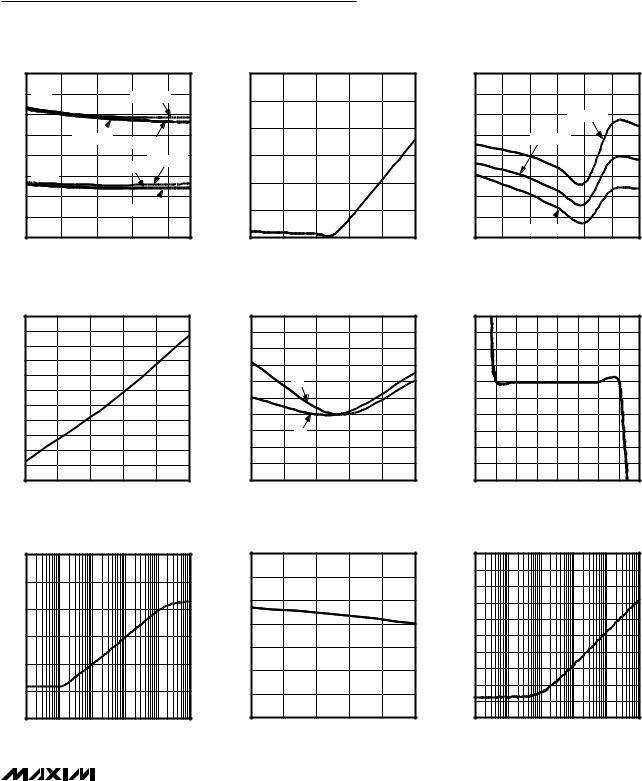
Typical Operating Characteristics
(VDD = 3V, VSS = VCM = 0V, RL to VDD / 2, TA = +25°C, unless otherwise noted.)
SUPPLY CURRENT |
SHUTDOWN SUPPLY CURRENT |
INPUT OFFSET VOLTAGE |
vs. SUPPLY VOLTAGE |
vs. TEMPERATURE |
vs. INPUT COMMON-MODE VOLTAGE |
|
9 |
|
|
|
|
toc01 |
|
12 |
|
|
|
|
|
|
|
|
|
|
8 |
DUAL |
|
TA = -40°C |
MAX9910 |
(nA) |
10 |
|
|
|
|
||||||
|
7 |
|
|
|
|
|
CURRENT |
|
|
6 |
|
TA = +85°C |
|
|
|
8 |
|
A) |
|
TA = +25°C |
|
|
||||
|
|
|
|
|||||
( |
5 |
|
|
|
TA = -40°C |
|
SUPPLY |
6 |
CC |
|
TA = +25°C |
|
|||||
|
|
|
|
|||||
I |
|
SINGLE |
|
|
|
|||
|
4 |
|
|
|
|
SHUTDOWN |
4 |
|
|
|
|
|
|
|
|||
|
|
|
|
|
|
|
||
|
3 |
|
|
|
|
|
|
|
|
2 |
|
|
TA = +85°C |
|
2 |
||
|
|
|
|
|
|
|
|
|
|
1 |
2.6 |
3.4 |
4.2 |
5.0 |
|
|
0 |
|
1.8 |
5.5 |
|
|
||||
|
|
|
VSUPPLY (V) |
|
|
|
|
|
|
|
|
|
|
toc02 |
|
1000 |
|
|
|
|
|
|
|
|
|
|
|
|
|
MAX9910 |
|
750 |
|
|
|
|
|
|
|
|
|
|
|
|
|
|
|
500 |
|
|
|
|
|
|
( V) |
250 |
|
|
|
|
|
|
0 |
|
|
|
|
|
|
|
OS |
|
|
|
|
|
|
|
|
|
|
|
|
|
|
|
V |
|
|
|
|
|
|
|
|
-250 |
|
|
|
|
|
|
|
-500 |
|
|
|
|
|
|
|
-750 |
-40 |
-15 |
10 |
35 |
60 |
85 |
-1000 |
|
|
|
||||||
TEMPERATURE (°C)
MAX9910 toc03 |
TA = -40°C |
TA = +25°C |
TA = +85°C |
0 |
0.5 |
1.0 |
1.5 |
2.0 |
2.5 |
3.0 |
VCM (V)
INPUT OFFSET VOLTAGE |
INPUT BIAS CURRENT |
INPUT BIAS CURRENT |
vs. TEMPERATURE |
vs. TEMPERATURE |
vs. INPUT COMMON-MODE VOLTAGE |
|
200 |
|
|
|
|
toc04 |
|
7 |
|
150 |
|
|
|
|
|
6 |
|
|
|
|
|
|
MAX9910 |
|
||
|
100 |
|
|
|
|
|
5 |
|
|
|
|
|
|
|
|
|
|
|
50 |
|
|
|
|
|
|
4 |
|
0 |
|
|
|
|
|
|
|
( V) |
|
|
|
|
|
|
3 |
|
-50 |
|
|
|
|
|
(pA) |
||
|
|
|
|
|
2 |
|||
|
|
|
|
|
|
|||
OS |
-100 |
|
|
|
|
|
B |
|
|
|
|
|
|
|
|||
V |
|
|
|
|
|
I |
1 |
|
|
-150 |
|
|
|
|
|
|
|
|
|
|
|
|
|
|
0 |
|
|
-200 |
|
|
|
|
|
|
|
|
|
|
|
|
|
|
|
|
|
-250 |
|
|
|
|
|
|
-1 |
|
|
|
|
|
|
|
|
|
|
-300 |
|
|
|
|
|
|
-2 |
|
-350 |
-15 |
10 |
35 |
60 |
|
|
-3 |
|
-40 |
85 |
|
|
|
|
|
|
|
toc05 |
|
5 |
|
|
|
|
|
|
4 |
|
|
|
|
|
|
MAX9910 |
|
|
|
|
|
|
|
|
3 |
|
|
|
|
|
|
|
|
|
|
|
|
|
|
|
|
2 |
|
|
IB- |
|
|
|
(pA) |
1 |
|
|
|
|
|
|
0 |
|
|
|
|
|
|
|
B |
|
|
|
|
|
|
|
|
|
|
|
|
|
|
|
I |
-1 |
|
|
|
|
|
|
|
|
|
|
IB+ |
|
|
|
|
-2 |
|
|
|
|
|
|
|
-3 |
|
|
|
|
|
|
|
-4 |
-40 |
-15 |
10 |
35 |
60 |
85 |
|
-5 |
|
|
|
|
|
|
|
|
|
|
MAX9910 toc06 |
-0.5 |
0 |
0.5 |
1.0 |
1.5 |
2.0 |
2.5 |
3.0 |
3.5 |
TEMPERATURE (°C) |
TEMPERATURE (°C) |
VCM (V) |
POWER-SUPPLY REJECTION RATIO |
COMMON-MODE REJECTION RATIO |
vs. FREQUENCY |
vs. TEMPERATURE |
0 |
|
|
|
|
MAX9910 toc07 |
140 |
-20 |
|
|
|
|
120 |
|
-40 |
|
|
|
|
|
100 |
|
|
|
|
CMRR (dB) |
|
|
|
|
|
|
|
80 |
|
-60 |
|
|
|
|
|
|
PSRR(dB) |
|
|
|
|
60 |
|
-80 |
|
|
|
|
|
40 |
|
|
|
|
|
|
|
-100 |
|
|
|
|
|
20 |
|
|
|
|
|
|
|
-120 |
|
|
|
|
|
0 |
0.1 |
1 |
10 |
100 |
1k |
10k |
|
|
|
|
|
|
toc08 |
|
0 |
|
|
|
|
|
|
-10 |
|
|
|
|
|
|
MAX9910 |
|
|
|
|
|
|
|
|
-20 |
|
|
|
|
|
|
|
|
|
|
|
|
|
|
|
|
-30 |
|
|
|
|
|
|
(dB) |
-40 |
|
|
|
|
|
|
|
|
|
|
|
|
|
|
CMRR |
-50 |
|
|
|
|
|
|
-60 |
|
|
|
|
|
|
|
|
|
|
|
|
|
|
|
|
-70 |
|
|
|
|
|
|
|
-80 |
|
|
|
|
|
|
|
-90 |
-40 |
-15 |
10 |
35 |
60 |
85 |
|
-100 |
|
|
FREQUENCY (Hz) |
TEMPERATURE (°C) |
COMMON-MODE REJECTION RATIO vs. FREQUENCY
|
|
|
|
|
MAX9910 toc09 |
1 |
10 |
100 |
1k |
10k |
100k |
FREQUENCY (Hz)
MAX9913–MAX9910
_______________________________________________________________________________________ 5
200kHz, 4µA, Rail-to-Rail I/O Op Amps with Shutdown
MAX9910–MAX9913
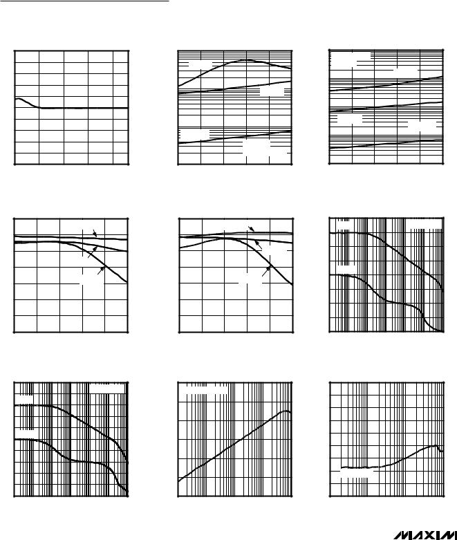
Typical Operating Characteristics (continued)
(VDD = 3V, VSS = VCM = 0V, RL to VDD / 2, TA = +25°C, unless otherwise noted.)
SLEW RATE
vs. SUPPLY VOLTAGE
|
0.6 |
|
|
|
|
toc10 |
|
0.5 |
|
|
|
|
|
|
|
|
|
|
MAX9910 |
|
|
0.4 |
|
|
|
|
|
|
|
|
|
|
|
|
S) |
0.3 |
|
|
|
|
|
(V/ |
0.2 |
|
|
|
|
|
RATE |
0.1 |
|
|
|
|
|
|
|
|
|
|
|
|
SLEW |
0 |
|
|
|
|
|
-0.1 |
|
|
|
|
|
|
|
|
|
|
|
|
|
|
-0.2 |
|
|
|
|
|
|
-0.3 |
|
|
|
|
|
|
-0.4 |
2.6 |
3.4 |
4.2 |
5.0 |
|
|
1.8 |
5.5 |
SUPPLY VOLTAGE (V)
OUTPUT-SWING HIGH |
OUTPUT-SWING LOW |
vs. TEMPERATURE |
vs. TEMPERATURE |
|
1000 |
|
|
|
|
toc11 |
10000 |
|
|
|
|
|
|
|
|
|
|
|
|
RL = 1kΩ |
|
|
|
MAX9910 |
(mV) |
|
(mV) |
|
|
|
|
|
1000 |
||
SWING |
100 |
|
|
|
RL = 5kΩ |
|
SWING |
|
|
|
|
|
|
|
|
||
VOLTAGE |
|
|
|
|
|
|
VOLTAGE |
100 |
|
|
|
|
|
|
|
||
OUTPUT |
10 |
|
|
|
|
|
OUTPUT |
|
RL = 100kΩ |
|
|
|
|
10 |
|||
|
|
|
RL TO VSS |
|
|
|||
|
|
|
|
|
|
|
||
|
|
|
|
VOH = VDD - VOUT |
|
|
|
|
|
1 |
|
|
|
|
|
|
1 |
|
-40 |
-15 |
10 |
35 |
60 |
85 |
|
|
VOL = VOUT - VSS |
|
toc12 |
RL TO VDD |
|
MAX9910 |
|
RL = 1kΩ |
|
|
|
|
RL = 5kΩ |
RL = 100kΩ |
|
|
|
-40 |
-15 |
10 |
35 |
60 |
85 |
TEMPERATURE (°C) |
TEMPERATURE (°C) |
OPEN-LOOP GAIN |
OPEN-LOOP GAIN |
vs. TEMPERATURE (RL TO VSS) |
vs. TEMPERATURE (RL TO VDD) |
|
140 |
|
|
RL = 100kΩ |
|
|
toc13 |
|
|
140 |
||
|
|
|
|
|
|
|
|
|
||||
|
120 |
|
|
|
|
|
|
|
MAX9910 |
|
|
120 |
|
|
|
|
|
|
|
|
|
|
|
|
|
|
100 |
|
|
|
|
|
|
|
|
|
|
100 |
(dB) |
80 |
|
|
RL = 5kΩ |
|
|
|
|
|
(dB) |
80 |
|
|
|
|
|
|
|
|
|
|
||||
VOL |
60 |
|
|
R |
L |
= 1kΩ |
|
|
|
|
VOL |
60 |
A |
|
|
|
|
|
|
|
|
A |
|||
|
|
|
|
|
|
|
|
|
|
|
||
|
40 |
|
|
|
|
|
|
|
|
|
|
40 |
|
20 |
|
|
|
|
|
|
|
|
|
|
20 |
|
0 |
|
|
|
|
|
|
|
|
|
|
0 |
|
-40 |
-15 |
10 |
35 |
|
60 |
85 |
|
|
|
||
|
|
|
TEMPERATURE (°C) |
|
|
|
|
|
|
|||
|
|
|
GAIN AND PHASE |
|
|
|
|
|
|
|||
|
vs. FREQUENCY (RL = 5kΩ, CLOAD = 100pF) |
|
|
|
||||||||
|
100 |
|
|
|
|
|
MAX9910 toc16 |
225 |
|
|
0 |
|
|
80 |
|
|
|
|
AV = 1000V/V |
|
180 |
|
|
|
|
|
GAIN |
|
|
|
|
|
|
|
|
|
||
|
60 |
|
|
|
|
|
|
135 |
|
|
-20 |
|
|
|
|
|
|
|
|
|
|
|
|||
|
|
|
|
|
|
|
|
|
|
|
||
|
40 |
|
|
|
|
|
|
|
90 |
PHASE (DEGREES) |
CROSSTALK (dB) |
-40 |
GAIN (dB) |
20 |
|
|
|
|
|
|
|
45 |
|||
PHASE |
|
|
|
|
|
|
|
|||||
0 |
|
|
|
|
|
|
0 |
-60 |
||||
|
|
|
|
|
|
|
||||||
-20 |
|
|
|
|
|
|
|
-45 |
|
|||
-40 |
|
|
|
|
|
|
|
-90 |
-80 |
|||
|
|
|
|
|
|
|
|
|
|
|||
|
|
|
|
|
|
|
|
|
|
|
||
|
-60 |
|
|
|
|
|
|
|
-135 |
|
|
-100 |
|
|
|
|
|
|
|
|
|
|
|
||
|
-80 |
|
|
|
|
|
|
|
-180 |
|
|
|
|
|
|
|
|
|
|
|
|
|
|
||
|
-100 |
|
|
|
|
|
|
|
-225 |
|
|
-120 |
|
1 |
10 |
100 |
1k |
10k |
100k |
1M |
|
|
|
||
|
|
|
FREQUENCY (Hz) |
|
|
|
|
|
|
|||
|
|
RL = 100kΩ |
|
toc14 |
|
80 |
|
|
|
|
|
|
|||
|
|
|
MAX9910 |
|
60 |
||
|
|
|
|
|
|
||
|
|
|
|
|
|
|
|
|
|
|
|
RL = 5kΩ |
|
|
40 |
|
|
|
|
|
|
|
|
|
|
|
|
|
|
(dB) |
20 |
|
|
|
|
|
|
0 |
|
|
|
|
RL = 1kΩ |
|
|
GAIN |
|
|
|
|
|
|
|
||
|
|
|
|
|
|
|
-20 |
|
|
|
|
|
|
|
-40 |
|
|
|
|
|
|
|
-60 |
|
|
|
|
|
|
|
-80 |
-40 |
-15 |
10 |
35 |
60 |
85 |
|
|
TEMPERATURE (°C)
|
|
CROSSTALK |
|
|
|
|
|
|
vs. FREQUENCY |
|
|
|
|
|
MAX9912/MAX9913 |
|
toc17 |
|
-5 |
|
|
|
|
|
|||
|
|
MAX9910 |
|
-15 |
||
|
|
|
|
|
||
|
|
|
|
|
-25 |
|
|
|
|
|
|
|
|
|
|
|
|
|
(dB) |
-35 |
|
|
|
|
|
-45 |
|
|
|
|
|
|
THD+N |
|
|
|
|
|
|
-55 |
|
|
|
|
|
|
|
|
|
|
|
|
|
|
-65 |
|
|
|
|
|
|
-75 |
|
|
|
|
|
|
-85 |
10 |
100 |
1k |
10k |
100k |
|
-95 |
|
|
|||||
FREQUENCY (Hz)
GAIN AND PHASE
vs. FREQUENCY (RL = ∞, CLOAD = 15pF)
|
|
|
|
|
MAX9910 toc15 |
180 |
|
|
|
GAIN |
|
|
AV = 1000V/V |
|
135 |
|
|
|
|
|
|
|
|
|
|
|
|
|
|
|
|
|
|
90 |
|
|
|
|
|
|
|
|
45 |
(DEGREES) |
|
PHASE |
|
|
|
|
|
0 |
|
|
|
|
|
|
|
|
||
|
|
|
|
|
|
|
-45 |
PHASE |
|
|
|
|
|
|
|
|
|
|
|
|
|
|
|
|
-90 |
|
|
|
|
|
|
|
|
-135 |
|
1 |
10 |
100 |
1k |
10k |
100k |
1M |
-180 |
|
|
|
|||||||
|
|
FREQUENCY (Hz) |
|
|
|
|
||
TOTAL HARMONIC DISTORTION
PLUS NOISE vs. FREQUENCY
MAX9910 toc18 |
VOUT = 2VP-P
10 |
100 |
1k |
10k |
FREQUENCY (Hz)
6_______________________________________________________________________________________
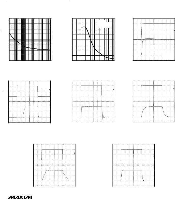
200kHz, 4µA, Rail-to-Rail I/O Op Amps with Shutdown
Typical Operating Characteristics (continued)
(VDD = 3V, VSS = VCM = 0V, RL to VDD / 2, TA = +25°C, unless otherwise noted.)
VOLTAGE-NOISE DENSITY vs. FREQUENCY
10,000 |
|
|
|
|
MAX9910 toc19 |
|
|
|
|
|
|
|
|
(nV/√Hz) |
|
|
|
|
|
|
VOLTAGE NOISE |
1000 |
|
|
|
|
|
|
|
|
|
|
|
|
|
100 |
|
|
|
|
|
|
1 |
10 |
100 |
1k |
10k |
100k |
FREQUENCY (Hz)
RESISTOR ISOLATION |
POWER-UP SETTLING TIME |
vs. CAPACITIVE LOAD |
|
8000 |
|
|
|
|
MAX9910 toc21 |
|
|
AV = 1V/V |
|
toc20 |
|
|
|
|
|
|
|
||
|
|
|
|
MAX9910 |
|
|
|
7000 |
|
FOR AV = 10V/V |
|
|
|
|
6000 |
|
NO RISO NEEDED |
|
VDD |
|
|
|
|
|
|
1V/div |
|
|
|
|
|
|
|
|
) |
5000 |
|
|
|
|
|
(Ω |
4000 |
|
|
|
|
|
ISO |
|
|
|
|
|
|
|
|
|
|
|
|
|
R |
|
|
|
|
|
|
|
3000 |
|
|
|
|
|
|
2000 |
|
|
|
|
OUTPUT |
|
|
|
|
|
500mV/div |
|
|
|
|
|
|
|
|
|
1000 |
|
|
|
|
IN+ = VDD / 2 |
|
0 |
|
|
|
|
AV = 1V/V |
|
|
|
|
|
500ns/div |
|
|
10 |
100 |
1000 |
10,000 |
||
|
|
|
CLOAD (pF) |
|
|
|
|
SMALL-SIGNAL PULSE RESPONSE |
SMALL-SIGNAL PULSE RESPONSE |
SHUTDOWN RESPONSE |
(CLOAD = 15pF) |
(CLOAD = 100pF) |
MAX9910 toc22 |
MAX9910 toc23 |
MAX9910 toc24 |
IN+ = VDD / 2
AV = 1V/V
SHDN
OUTPUT
|
|
|
|
|
|
|
|
3V |
|
AV = 1V/V |
|
|
|
AV = 10V/V |
|
|
|
|
|
|
|
|
|
IN+ |
|
|
|
IN+ |
|
|
|
50mV/div |
|
|
|
5mV/div |
|
|
|
0V |
|
|
|
|
|
|
|
1.5V |
|
|
|
|
|
|
|
OUTPUT |
|
|
|
OUTPUT |
|
|
|
50mV/div |
|
|
|
50mV/div |
|
|
|
0V |
|
|
|
|
|
|
|
|
|
|
|
|
|
|
|
20 s/div |
10 s/div |
20 s/div |
MAX9913–MAX9910
|
LARGE-SIGNAL PULSE RESPONSE |
|
LARGE-SIGNAL PULSE RESPONSE |
||||
|
(CLOAD = 15pF) |
|
(CLOAD = 100pF) |
||||
|
|
MAX9910 toc25 |
|
|
MAX9910 toc26 |
||
|
|
|
|
|
|
|
|
|
|
AV = 1V/V |
|
|
|
AV = 10V/V |
|
IN+ |
IN+ |
||||||
1V/div |
100mV/div |
||||||
OUTPUT |
OUTPUT |
||
1V/div |
1V/div |
||
|
|
|
|
|
10 s/div |
|
100 s/div |
_______________________________________________________________________________________ 7
MAX9910–MAX9913
200kHz, 4µA, Rail-to-Rail I/O Op Amps with Shutdown
Typical Operating Characteristics (continued)
(VDD = 3V, VSS = VCM = 0V, RL to VDD / 2, TA = +25°C, unless otherwise noted.)
SMALL-SIGNAL GAIN vs. FREQUENCY
|
10 |
AV = +1V/V |
|
toc27 |
|
8 |
|
||
|
VOUT = 100mVP-P |
|
MAX9910 |
|
|
6 |
CLOAD = 15pF |
|
|
|
|
|
|
|
|
4 |
|
|
|
(dB) |
2 |
|
|
|
0 |
|
|
|
|
GAIN |
|
|
|
|
-2 |
|
|
|
|
|
|
|
|
|
|
-4 |
|
|
|
|
-6 |
|
|
|
|
-8 |
|
|
|
|
-10 |
|
|
|
|
1 |
10 |
100 |
1000 |
FREQUENCY (kHz)
GAIN (dB)
|
LARGE-SIGNAL GAIN |
|
|
vs. FREQUENCY |
|
4 |
AV = +1V/V |
toc28 |
|
||
|
CLOAD = 15pF |
MAX9910 |
3 |
VOUT = 2VP-P |
|
2 |
|
|
1 |
|
|
0 |
|
|
-1 |
|
|
-2 |
|
|
-3 |
|
|
-4 |
|
|
1 |
10 |
100 |
|
FREQUENCY (kHz) |
|
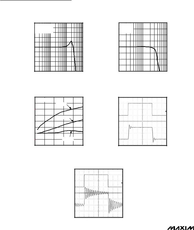
PERCENT OVERSHOOT |
OUTPUT WAVEFORM WITH RISO |
vs. CAPACITIVE LOAD |
(CLOAD = 100pF, RISO = 6.2kΩ) |
|
4.0 |
|
|
|
|
toc29 |
|
MAX9910 toc30 |
|
AV = 1V/V |
|
|
|
AV |
= 1V/V |
||
|
|
|
|
|
||||
|
3.5 |
|
RL = 1MΩ |
|
MAX9910 |
|||
|
|
|
|
IN+ |
|
|||
|
|
|
|
|
|
|
|
|
|
3.0 |
|
|
|
|
|
50mV/div |
|
(%) |
2.5 |
|
|
RL = 100kΩ |
|
|
|
|
OVERSHOOT |
|
|
|
|
|
|
||
1.5 |
|
|
|
|
|
|
||
|
|
|
|
|
|
|
||
|
2.0 |
|
|
|
|
|
|
|
|
|
|
|
|
|
|
OUTPUT |
|
|
1.0 |
|
|
|
|
|
50mV/div |
|
|
|
|
|
|
|
|
|
|
|
0.5 |
|
|
RL = 10kΩ |
|
|
|
|
|
0 |
|
|
|
|
|
|
|
|
0 |
20 |
40 |
60 |
80 |
100 |
|
20µs/div |
|
|
|
CLOAD (pF) |
|
|
|
|
|
|
|
|
|
|
|
OUTPUT WAVEFORM WITHOUT RISO |
|
|
|
|
|
|
|
|
|
(CLOAD = 100pF) |
|
|
|
|
|
|
|
|
MAX9910 toc31 |
|
|
|
|
|
|
|
|
AV = 1V/V |
|
|
|
|
|
|
IN+ |
|
|
|
|
|
|
|
50mV/div |
|
|
|
|
OUTPUT 50mV/div
20µs/div
8_______________________________________________________________________________________
200kHz, 4µA, Rail-to-Rail I/O Op Amps with Shutdown
Pin Description
|
|
PIN |
|
|
|
|
|
|
|
|
|
NAME |
FUNCTION |
MAX9911 |
MAX9910 |
MAX9911 |
MAX9912 |
MAX9913 |
||
(WLP) |
(SC70) |
|
|
|||
|
|
|
|
|
||
|
|
|
|
|
|
|
A1 |
1 |
1 |
— |
— |
IN+ |
Noninverting Amplifier Input |
|
|
|
|
|
|
|
A2 |
2 |
2 |
4 |
4 |
VSS |
Negative Supply Voltage |
B1 |
3 |
3 |
— |
— |
IN- |
Inverting Amplifier Input |
|
|
|
|
|
|
|
C1 |
4 |
4 |
— |
— |
OUT |
Amplifier Output |
|
|
|
|
|
|
|
B2 |
5 |
6 |
8 |
10 |
VDD |
Positive Supply Voltage |
C2 |
— |
5 |
— |
— |
SHDN |
Shutdown |
|
|
|
|
|
|
|
— |
— |
— |
1 |
1 |
OUTA |
Amplifier Output Channel A |
— |
— |
— |
2 |
2 |
INA- |
Inverting Amplifier Input Channel A |
|
|
|
|
|
|
|
— |
— |
— |
3 |
3 |
INA+ |
Noninverting Amplifier Input Channel A |
|
|
|
|
|
|
|
— |
— |
— |
— |
5 |
SHDNA |
Shutdown Channel A |
— |
— |
— |
— |
6 |
SHDNB |
Shutdown Channel B |
|
|
|
|
|
|
|
— |
— |
— |
5 |
7 |
INB+ |
Noninverting Amplifier Input Channel B |
— |
— |
— |
6 |
8 |
INB- |
Inverting Amplifier Input Channel B |
|
|
|
|
|
|
|
— |
— |
— |
7 |
9 |
OUTB |
Amplifier Output Channel B |
|
|
|
|
|
|
|
MAX9913–MAX9910
Detailed Description
Featuring a maximized ratio of GBW to supply current, low operating supply voltage, low input bias current, and rail-to-rail inputs and outputs, the MAX9910– MAX9913 are an excellent choice for precision or gen- eral-purpose, low-current, low-voltage, battery-powered applications. These CMOS devices consume an ultralow 4µA (typ) supply current and a 200µV (typ) offset voltage. For additional power conservation, the MAX9911/MAX9913 feature a low-power shutdown mode that reduces supply current to 1nA (typ), and puts the amplifiers’ output in a high-impedance state. These devices are unity-gain stable with a 200kHz GBW product, driving capacitive loads up to 30pF. The capacitive load can be increased to 250pF when the amplifier is configured for a 10V/V gain.
Rail-to-Rail Inputs and Outputs
All of the MAX9910–MAX9913 amplifiers have a parallelconnected n- and p-channel differential input stage that allows an input common-mode voltage range that extends 100mV beyond the positive and negative supply rails, with excellent common-mode rejection.
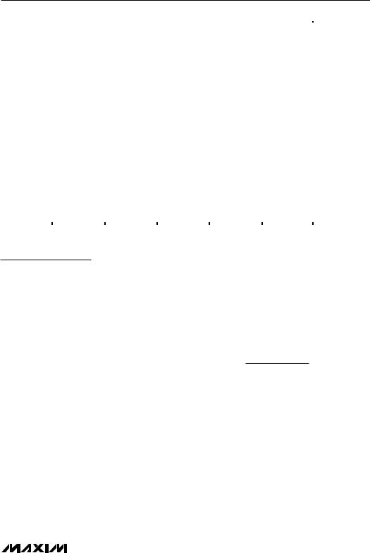
The MAX9910–MAX9913 are capable of driving the output to within 5mV of both supply rails with a 100kΩ
load. These devices can drive a 5kΩ load with swings to within 60mV of the rails. Figure 1 shows the output voltage swing of the MAX9910–MAX9913 configured as a unity-gain buffer powered from a single 3V supply.
Low Input Bias Current
The MAX9910–MAX9913 feature ultra-low 1pA (typ) input bias current. The variation in the input bias current is minimal with changes in the input voltage due to very high input impedance (in the order of 1GΩ).
Applications Information
Driving Capacitive Loads
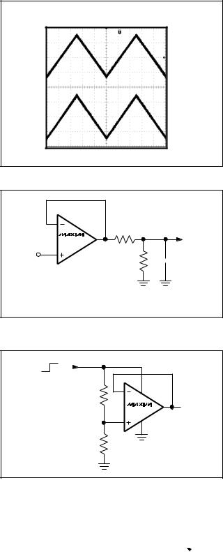
The MAX9910–MAX9913 amplifiers are unity-gain stable for loads up to 30pF. However, the capacitive load can be increased to 250pF when the amplifier is configured for a minimum gain of 10V/V. Applications that require greater capacitive-drive capability should use an isolation resistor between the output and the capacitive load (Figure 2). Also, in unity-gain applications with relatively small RL (approximately 5kΩ), the capacitive load can be increased up to 200pF.
Power-Supply Considerations
The MAX9910–MAX9913 are optimized for single 1.8V to 5.5V supply operation. A high amplifier power-supply
_______________________________________________________________________________________ 9
MAX9910–MAX9913
200kHz, 4µA, Rail-to-Rail I/O Op Amps with Shutdown
rejection ratio of 95dB (typ) allows the devices to be powered directly from a battery, simplifying design and extending battery life.
Power-Up Settling Time
The MAX9910–MAX9913 typically require 5µs after power-up. Supply settling time depends on the supply voltage, the value of the bypass capacitor, the output impedance of the incoming supply, and any lead resistance or inductance between components. Op-amp settling time depends primarily on the output voltage and is slew-rate limited. Figure 3 shows the MAX991_ in a noninverting voltage follower configuration with the input held at midsupply. The output settles in approximately 18µs for VDD = 3V (see the Typical Operating Characteristics for power-up settling time).
Shutdown Mode
The MAX9911/MAX9913 feature active-low shutdown inputs. The MAX9911/MAX9913 enter shutdown in 2µs (typ) and exit in 30µs (typ). The amplifiers’ outputs are in a high-impedance state in shutdown mode. Drive SHDN low to enter shutdown. Drive SHDN high to enable the amplifier. The MAX9913 dual-amplifier features separate shutdown inputs. Shut down both amplifiers for the lowest quiescent current.
Power-Supply Bypassing and Layout
To minimize noise, bypass VDD with a 0.1µF capacitor to ground, as close to the pin as possible.
Good layout techniques optimize performance by decreasing the amount of stray capacitance and inductance to the op amps’ inputs and outputs. Minimize stray capacitance and inductance by placing external components close to the IC.
RAIL-TO-RAIL OUTPUT VOLTAGE RANGE
3V
IN_
1V/div
0V
3V
OUT_
1V/div
0V
200 s/div
Figure 1. Rail-to-Rail Output Voltage Range
MAX9910– |
MAX9913 |
RISO
RL  CL
CL
RL
AV = RL + RISO ≈ 1V/V
Figure 2. Using a Resistor to Isolate a Capacitive Load from the Op Amp
5.5V |
|
|
0V |
|
|
IN- |
VDD |
|
100kΩ |
|
|
|
MAX991_ |
OUT |
|
|
|
IN+ |
VSS |
|
|
|
|
100kΩ |
|
|
Figure 3. Power-Up Test Configuration
10 ______________________________________________________________________________________ 


