

бакМИТ_КП2015 / Компоненты по вариантам / Операционные_усилители / OP296HRU
.pdfa |
Micropower, Rail-to-Rail Input and Output |
|
Operational Amplifiers |
||
|
|
|
|
|
OP196/OP296/OP496 |
|
|
|
FEATURES
Rail-to-Rail Input and Output Swing Low Power: 60 A/Amplifier
Gain Bandwidth Product: 450 kHz Single-Supply Operation: 3 V to 12 V Low Offset Voltage: 300 V max
High Open-Loop Gain: 500 V/mV Unity-Gain Stable
No Phase Reversal
|
|
PIN CONFIGURATIONS |
|
|
|
|
||||
8-Lead Narrow-Body SO |
8-Lead Narrow-Body SO |
|||||||||
|
|
|
|
|
|
|
|
|
|
V+ |
|
|
|
|
|
|
|
|
|
|
|
NULL |
1 |
|
8 |
NC |
OUT A |
|
1 |
|
8 |
|
|
|
|
|
|
|
|
|
|
|
OUT B |
–IN A |
2 |
OP196 |
7 |
V+ |
–IN A |
|
2 |
OP296 |
7 |
|
|
|
|
OUT A |
|
|
|
|
|
||
+IN A |
3 |
|
6 |
+IN A |
|
3 |
|
6 |
–IN B |
|
|
|
|
|
|
V– |
|
|
|
|
+IN B |
V– |
4 |
|
5 |
NULL |
|
4 |
|
5 |
||
|
|
|
|
|
|
|
|
|
|
|
NC = NO CONNECT
APPLICATIONS
Battery Monitoring
Sensor Conditioners
Portable Power Supply Control
Portable Instrumentation
GENERAL DESCRIPTION
The OP196 family of CBCMOS operational amplifiers features micropower operation and rail-to-rail input and output ranges.
The extremely low power requirements and guaranteed operation from 3 V to 12 V make these amplifiers perfectly suited to monitor battery usage and to control battery charging. Their dynamic performance, including 26 nV/√Hz voltage noise density, recommends them for battery-powered audio applications. Capacitive loads to 200 pF are handled without oscillation.
The OP196/OP296/OP496 are specified over the HOT extended industrial (–40°C to +125°C) temperature range. 3 V operation is specified over the 0°C to 125°C temperature range.
The single OP196 and the dual OP296 are available in 8-lead SO-8 surface mount packages. The dual OP296 is available in 8-lead PDIP. The quad OP496 is available in 14-lead plastic DIP and narrow SO-14 surface-mount packages.
8-Lead TSSOP
1 |
|
8 |
V+ |
|
OUT A |
|
|
|
|
–IN A |
|
OP296 |
|
OUT B |
+IN A |
|
|
–IN B |
|
V– |
|
|
|
+IN B |
|
4 |
|
5 |
|
|
|
|
||
14-Lead Narrow-Body SO
|
|
|
|
|
OUT A |
1 |
|
14 |
OUT D |
–IN A |
|
|
|
|
2 |
|
13 |
–IN D |
|
+IN A |
|
|
|
+IN D |
3 |
OP496 |
12 |
||
V+ |
|
|
V– |
|
4 |
11 |
|||
+IN B |
|
|
|
+IN C |
5 |
|
10 |
||
–IN B |
|
|
|
–IN C |
6 |
|
9 |
||
|
|
|
|
OUT C |
OUT B |
7 |
|
8 |
|
|
|
|
|
|
8-Lead Plastic DIP
OUT A |
1 |
OP296 |
8 |
V+ |
–IN A |
2 |
|
7 |
OUT B |
+IN A |
3 |
|
6 |
–IN B |
V– |
4 |
|
5 |
+IN B |
14-Lead Plastic DIP
OUT A |
1 |
|
14 |
OUT D |
–IN A |
2 |
|
13 |
–IN D |
+IN A |
3 |
|
12 |
+IN D |
V+ |
4 |
OP496 |
11 |
V– |
+IN B |
5 |
|
10 |
+IN C |
–IN B |
6 |
|
9 |
–IN C |
OUT B |
7 |
|
8 |
OUT C |
14-Lead TSSOP
(RU Suffix)
|
1 |
|
14 |
|
OUT A |
|
|
|
OUT D |
–IN A |
|
|
|
–IN D |
+IN A |
|
OP496 |
|
+IN D |
V+ |
|
|
V– |
|
+IN B |
|
|
|
+IN C |
–IN B |
|
|
|
–IN C |
OUT B |
|
|
|
OUT C |
|
7 |
|
8 |
|
|
|
|
||
REV. C
Information furnished by Analog Devices is believed to be accurate and reliable. However, no responsibility is assumed by Analog Devices for its use, nor for any infringements of patents or other rights of third parties that may result from its use. No license is granted by implication or otherwise under any patent or patent rights of Analog Devices.
One Technology Way, P.O. Box 9106, Norwood, MA 02062-9106, U.S.A.
Tel: 781/329-4700 |
www.analog.com |
Fax: 781/326-8703 |
© Analog Devices, Inc., 2002 |
OP196/OP296/OP496–SPECIFICATIONS
ELECTRICAL SPECIFICATIONS (@ VS = 5.0 V, VCM = 2.5 V, TA = 25 C, unless otherwise noted.)
Parameter |
Symbol |
Conditions |
|
Min |
Typ |
Max |
Unit |
|
|
|
|
|
|
|
|
INPUT CHARACTERISTICS |
|
|
|
|
|
|
µV |
Offset Voltage |
VOS |
OP196G, OP296G, OP496G |
|
35 |
300 |
||
|
|
–40°C ≤ TA ≤ +125°C |
|
|
650 |
µV |
|
|
|
OP296H, OP496H |
|
|
800 |
µV |
|
|
|
–40°C ≤ TA |
≤ +125°C |
|
|
1.2 |
mV |
Input Bias Current |
IB |
–40°C ≤ TA |
≤ +125°C |
|
±10 |
±50 |
nA |
Input Offset Current |
IOS |
–40°C ≤ TA ≤ +125°C |
|
±1.5 |
± 8 |
nA |
|
|
|
|
|
±20 |
nA |
||
Input Voltage Range |
VCM |
0 V ≤ VCM ≤ 5.0 V, |
0 |
|
5.0 |
V |
|
Common-Mode Rejection Ratio |
CMRR |
|
|
|
|
||
|
|
–40°C ≤ TA ≤ +125°C |
65 |
|
|
dB |
|
Large Signal Voltage Gain |
AVO |
RL = 100 kΩ, |
|
|
|
|
|
|
|
0.30 V ≤ VOUT ≤ 4.7 V, |
|
|
|
|
|
|
|
–40°C ≤ TA |
≤ +125°C |
150 |
200 |
|
V/mV |
Long-Term Offset Voltage |
VOS |
G Grade, Note 1 |
|
|
550 |
µV |
|
|
|
H Grade, Note 1 |
|
|
1 |
mV |
|
Offset Voltage Drift |
∆VOS/∆T |
G Grade, Note 2 |
|
1.5 |
|
µV/°C |
|
|
|
H Grade, Note 2 |
|
2 |
|
µV/°C |
|
OUTPUT CHARACTERISTICS |
|
IL = –100 µA |
|
|
|
|
|
Output Voltage Swing High |
VOH |
4.85 |
4.92 |
|
V |
||
|
|
IL = 1 mA |
|
4.30 |
4.56 |
|
V |
Output Voltage Swing Low |
VOL |
IL = 2 mA |
|
|
4.1 |
|
V |
IL = –1 mA |
|
|
36 |
70 |
mV |
||
|
|
IL = –1 mA |
|
|
350 |
550 |
mV |
|
|
IL = –2 mA |
|
|
750 |
|
mV |
Output Current |
IOUT |
|
|
|
± 4 |
|
mA |
POWER SUPPLY |
|
±2.5 V ≤ VS |
≤ ±6 V, |
|
|
|
|
Power Supply Rejection Ratio |
PSRR |
|
|
|
|
||
|
|
–40°C ≤ TA |
≤ +125°C |
85 |
|
|
dB |
Supply Current per Amplifier |
ISY |
VOUT = 2.5 V, RL = ∞ |
|
|
60 |
µA |
|
|
|
–40°C ≤ TA ≤ +125°C |
|
45 |
80 |
µA |
|
DYNAMIC PERFORMANCE |
|
RL = 100 kΩ |
|
|
|
V/µs |
|
Slew Rate |
SR |
|
0.3 |
|
|||
Gain Bandwidth Product |
GBP |
|
|
|
350 |
|
kHz |
Phase Margin |
øm |
|
|
|
47 |
|
Degrees |
NOISE PERFORMANCE |
|
|
|
|
|
|
µV p-p |
Voltage Noise |
en p-p |
0.1 Hz to 10 Hz |
|
0.8 |
|
||
Voltage Noise Density |
en |
f = 1 kHz |
|
|
26 |
|
nV/√Hz |
Current Noise Density |
in |
f = 1 kHz |
|
|
0.19 |
|
pA/√Hz |
NOTES
1Long-term offset voltage is guaranteed by a 1,000 hour life test performed on three independent lots at 12 5°C, with an LTPD of 1.3. 2Offset voltage drift is the average of the –40°C to +25°C delta and the +25°C to +125°C delta.
Specifications subject to change without notice.
–2– |
REV. C |
OP196/OP296/OP496
ELECTRICAL SPECIFICATIONS (@ VS = 3.0 V, VCM = 1.5 V, TA = 25 C, unless otherwise noted.)
Parameter |
Symbol |
Conditions |
Min |
Typ |
Max |
Unit |
|
|
|
|
|
|
|
INPUT CHARACTERISTICS |
|
|
|
|
|
µV |
Offset Voltage |
VOS |
OP196G, OP296G, OP496G |
|
35 |
300 |
|
|
|
0°C ≤ TA ≤ 125°C |
|
|
650 |
µV |
|
|
OP296H, OP496H |
|
|
800 |
µV |
|
|
0°C ≤ TA ≤ 125°C |
|
|
1.2 |
mV |
Input Bias Current |
IB |
|
|
± 10 |
± 50 |
nA |
Input Offset Current |
IOS |
|
|
± 1 |
± 8 |
nA |
Input Voltage Range |
VCM |
0 V ≤ VCM ≤ 3.0 V, |
0 |
|
3.0 |
V |
Common-Mode Rejection Ratio |
CMRR |
|
|
|
|
|
|
|
0°C ≤ TA ≤ 125°C |
60 |
|
|
dB |
Large Signal Voltage Gain |
AVO |
RL = 100 kΩ |
80 |
200 |
|
V/mV |
Long-Term Offset Voltage |
VOS |
G Grade, Note 1 |
|
|
550 |
µV |
|
|
H Grade, Note 1 |
|
|
1 |
mV |
Offset Voltage Drift |
∆VOS/∆T |
G Grade, Note 2 |
|
1.5 |
|
µV/°C |
|
|
H Grade, Note 2 |
|
2 |
|
µV/°C |
OUTPUT CHARACTERISTICS |
|
IL = 100 µA |
|
|
|
|
Output Voltage Swing High |
VOH |
2.85 |
|
|
V |
|
Output Voltage Swing Low |
VOL |
IL = –100 µA |
|
|
70 |
mV |
POWER SUPPLY |
|
VOUT = 1.5 V, RL = ∞ |
|
|
|
µA |
Supply Current per Amplifier |
ISY |
|
40 |
60 |
||
|
|
0°C ≤ TA ≤ 125°C |
|
|
80 |
µA |
DYNAMIC PERFORMANCE |
|
RL = 100 kΩ |
|
|
|
V/µs |
Slew Rate |
SR |
|
0.25 |
|
||
Gain Bandwidth Product |
GBP |
|
|
350 |
|
kHz |
Phase Margin |
øm |
|
|
45 |
|
Degrees |
NOISE PERFORMANCE |
|
|
|
|
|
µV p-p |
Voltage Noise |
en p-p |
0.1 Hz to 10 Hz |
|
0.8 |
|
|
Voltage Noise Density |
en |
f = 1 kHz |
|
26 |
|
nV/√Hz |
Current Noise Density |
in |
f = 1 kHz |
|
0.19 |
|
pA/√Hz |
NOTES
1Long-term offset voltage is guaranteed by a 1,000 hour life test performed on three independent lots at 12 5°C, with an LTPD of 1.3. 2Offset voltage drift is the average of the 0°C to 25°C delta and the 25°C to 125°C delta.
Specifications subject to change without notice.
REV. C |
–3– |
OP196/OP296/OP496
ELECTRICAL SPECIFICATIONS (@ VS = 12.0 V, VCM = 6 V, TA = 25 C, unless otherwise noted.)
Parameter |
Symbol |
Conditions |
Min |
Typ |
Max |
Unit |
|
|
|
|
|
|
|
INPUT CHARACTERISTICS |
|
|
|
|
|
µV |
Offset Voltage |
VOS |
OP196G, OP296G, OP496G |
|
35 |
300 |
|
|
|
0°C ≤ TA ≤ 125°C |
|
|
650 |
µV |
|
|
OP296H, OP496H |
|
|
800 |
µV |
|
|
0°C ≤ TA ≤ 125°C |
|
|
1.2 |
mV |
Input Bias Current |
IB |
–40°C ≤ TA ≤ +125°C |
|
± 10 |
± 50 |
nA |
Input Offset Current |
IOS |
–40°C ≤ TA ≤ +125°C |
|
± 1 |
± 8 |
nA |
|
|
|
|
± 15 |
nA |
|
Input Voltage Range |
VCM |
0 V ≤ VCM ≤ 12 V, |
0 |
|
12 |
V |
Common-Mode Rejection Ratio |
CMRR |
|
|
|
|
|
|
|
–40°C ≤ TA ≤ +125°C |
65 |
|
|
dB |
Large Signal Voltage Gain |
AVO |
RL = 100 kΩ |
300 |
1000 |
|
V/mV |
Long-Term Offset Voltage |
VOS |
G Grade, Note 1 |
|
|
550 |
µV |
|
|
H Grade, Note 1 |
|
|
1 |
mV |
Offset Voltage Drift |
∆VOS/∆T |
G Grade, Note 2 |
|
1.5 |
|
µV/°C |
|
|
H Grade, Note 2 |
|
2 |
|
µV/°C |
OUTPUT CHARACTERISTICS |
|
IL = 100 µA |
|
|
|
|
Output Voltage Swing High |
VOH |
11.85 |
|
|
V |
|
Output Voltage Swing Low |
VOL |
IL = 1 mA |
11.30 |
|
|
V |
IL = –1 mA |
|
|
70 |
mV |
||
|
|
IL = –1 mA |
|
± 4 |
550 |
mV |
Output Current |
IOUT |
|
|
|
mA |
|
POWER SUPPLY |
|
VOUT = 6 V, RL = ∞ |
|
|
|
µA |
Supply Current per Amplifier |
ISY |
|
|
60 |
||
|
|
–40°C ≤ TA ≤ +125°C |
|
|
80 |
µA |
Supply Voltage Range |
VS |
|
3 |
|
12 |
V |
DYNAMIC PERFORMANCE |
|
RL = 100 kΩ |
|
|
|
V/µs |
Slew Rate |
SR |
|
0.3 |
|
||
Gain Bandwidth Product |
GBP |
|
|
450 |
|
kHz |
Phase Margin |
øm |
|
|
50 |
|
Degrees |
NOISE PERFORMANCE |
|
|
|
|
|
µV p-p |
Voltage Noise |
en p-p |
0.1 Hz to 10 Hz |
|
0.8 |
|
|
Voltage Noise Density |
en |
f = 1 kHz |
|
26 |
|
nV/√Hz |
Current Noise Density |
in |
f = 1 kHz |
|
0.19 |
|
pA/√Hz |
NOTES
1Long-term offset voltage is guaranteed by a 1,000 hour life test performed on three independent lots at 12 5°C, with an LTPD of 1.3. 2Offset voltage drift is the average of the –40°C to +25°C delta and the +25°C to +125°C delta.
Specifications subject to change without notice.
–4– |
REV. C |

OP196/OP296/OP496
ABSOLUTE MAXIMUM RATINGS1 |
|
|
|
||
Supply Voltage . . . . . . . . . . . |
. . . . . . . |
. . . . . . |
. . . . |
. . . . . . 15 V |
|
Input Voltage2 . . . . . . . . . . . |
. . . . . . . |
. . . . . . |
. . . . |
. . . . . . 15 V |
|
Differential Input Voltage2 . |
. . . . . . . |
. . . . . . |
. . . . |
. . . . . . 15 V |
|
Output Short Circuit Duration . . . . . |
. . . . . . |
. . . . |
. . Indefinite |
||
Storage Temperature Range |
|
|
–65°C to +150°C |
||
P, S, RU Package . . . . . . . |
. . . . . . . |
. . . . . . |
|||
Operating Temperature Range |
|
–40°C to +125°C |
|||
OP196G, OP296G, OP496G, H . . |
. . . . . |
||||
Junction Temperature Range |
|
|
–65°C to +150°C |
||
P, S, RU Package . . . . . . . |
. . . . . . . |
. . . . . |
|||
Lead Temperature Range (Soldering, 60 sec) |
. . . . |
. . . . 300°C |
|||
|
|
|
|
|
|
Package Type |
|
JA3 |
JC |
|
Unit |
8-Lead Plastic DIP |
|
103 |
43 |
|
°C/W |
8-Lead SOIC |
|
158 |
43 |
|
°C/W |
8-Lead TSSOP |
|
240 |
43 |
|
°C/W |
14-Lead Plastic DIP |
|
83 |
39 |
|
°C/W |
14-Lead SOIC |
|
120 |
36 |
|
°C/W |
14-Lead TSSOP |
|
180 |
35 |
|
°C/W |
|
|
|
|
|
|
NOTES
1Absolute maximum ratings apply to both DICE and packaged parts, unless otherwise noted.
2For supply voltages less than 15 V, the absolute maximum input voltage is equal to the supply voltage.
3θJA is specified for the worst case conditions, i.e., θJA is specified for device in socket for P-DIP package; θJA is specified for device soldered in circuit board for SOIC and TSSOP packages.
ORDERING GUIDE
|
Temperature |
Package |
Package |
Model |
Range |
Description |
Option |
|
|
|
|
OP196GS |
–40°C to +125°C |
8-Lead SOIC |
SO-8 |
OP296GP* |
–40°C to +125°C |
8-Lead Plastic DIP |
N-8 |
OP296GS |
–40°C to +125°C |
8-Lead SOIC |
SO-8 |
OP296HRU |
–40°C to +125°C |
8-Lead TSSOP |
RU-8 |
OP496GP* |
–40°C to +125°C |
14-Lead Plastic DIP |
N-14 |
OP496GS |
–40°C to +125°C |
14-Lead SOIC |
SO-14 |
OP496HRU |
–40°C to +125°C |
14-Lead TSSOP |
RU-14 |
|
|
|
|
*Not for new design, obsolete April 2002.
CAUTION
ESD (electrostatic discharge) sensitive device. Electrostatic charges as high as 4000 V readily accumulate on the human body and test equipment and can discharge without detection. Although the OP196/OP296/OP496 feature proprietary ESD protection circuitry, permanent damage may occur on devices subjected to high-energy electrostatic discharges. Therefore, proper ESD precautions are recommended to avoid performance degradation or loss of functionality.
WARNING!
ESD SENSITIVE DEVICE
REV. C |
–5– |
OP196/OP296/OP496–Typical Performance Characteristics
|
250 |
|
|
|
|
|
|
|
|
|
|
|
|
|
|
|
|
|
|
|
|
|
|
|
|
|
|
|
|
|
|
|
|
|
|
|
|
|
|
|
|
|
|
|
|
|
|
|
|
|
|
|
|
|
VS |
= 3V |
|
|
|
|
|
|
|
200 |
|
|
|
|
|
|
|
|
|
|
|
TA = 25 C |
|
|
|
|
|
||
|
|
|
|
|
|
|
|
|
|
|
|
|
|
|
|
|||||
– Amplifiers |
|
|
|
|
|
|
|
|
|
|
|
|
COUNT = 400 |
|
|
|
|
|
||
150 |
|
|
|
|
|
|
|
|
|
|
|
|
|
|
|
|
|
|
|
|
|
|
|
|
|
|
|
|
|
|
|
|
|
|
|
|
|
|
|
||
|
|
|
|
|
|
|
|
|
|
|
|
|
|
|
|
|
|
|
||
|
|
|
|
|
|
|
|
|
|
|
|
|
|
|
|
|
|
|
|
|
QUANTITY |
100 |
|
|
|
|
|
|
|
|
|
|
|
|
|
|
|
|
|
|
|
|
|
|
|
|
|
|
|
|
|
|
|
|
|
|
|
|
|
|
||
|
|
|
|
|
|
|
|
|
|
|
|
|
|
|
|
|
|
|
|
|
|
50 |
|
|
|
|
|
|
|
|
|
|
|
|
|
|
|
|
|
|
|
|
|
|
|
|
|
|
|
|
|
|
|
|
|
|
|
|
|
|
|
|
|
0 |
|
|
|
|
|
|
|
|
|
|
|
|
|
|
|
|
|
|
|
|
|
|
|
|
|
|
|
|
|
|
|
|
|
|
|
|
|
|
|
|
|
|
|
|
|
|
|
|
|
|
|
|
|
|
|
|
|
|
|
|
|
|
–250 –200 |
–150 –100 –50 |
0 |
50 |
100 150 |
200 |
250 |
|||||||||||||
|
|
|
|
|
|
INPUT OFFSET VOLTAGE – V |
|
|
|
|
|
|||||||||
|
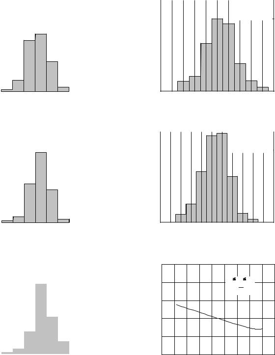
TPC 1. Input Offset Voltage Distribution |
|||||||||||||||||||
|
250 |
|
|
|
|
|
|
|
|
|
|
|
|
|
|
|
|
|
|
|
|
|
|
|
|
|
|
|
|
|
|
|
|
|
|
|
|
|
|
|
|
|
|
|
|
|
|
|
|
|
|
|
|
|
|
|
|
|
|
|
|
|
|
|
|
|
|
|
|
|
|
|
|
|
VS |
= 5V |
|
|
|
|
|
|
|
|
200 |
|
|
|
|
|
|
|
|
|
|
|
TA = 25 C |
|
|
|
|
|
||
|
|
|
|
|
|
|
|
|
|
|
|
|
|
|
|
|
||||
Amplifiers– |
|
|
|
|
|
|
|
|
|
|
|
|
COUNT = 400 |
|
|
|
|
|||
150 |
|
|
|
|
|
|
|
|
|
|
|
|
|
|
|
|
|
|
|
|
|
|
|
|
|
|
|
|
|
|
|
|
|
|
|
|
|
|
|
||
QUANTITY |
|
|
|
|
|
|
|
|
|
|
|
|
|
|
|
|
|
|
|
|
100 |
|
|
|
|
|
|
|
|
|
|
|
|
|
|
|
|
|
|
|
|
|
|
|
|
|
|
|
|
|
|
|
|
|
|
|
|
|
|
|
|
|
|
50 |
|
|
|
|
|
|
|
|
|
|
|
|
|
|
|
|
|
|
|
|
|
|
|
|
|
|
|
|
|
|
|
|
|
|
|
|
|
|
|
|
|
0 |
|
|
|
|
|
|
|
|
|
|
|
|
|
|
|
|
|
|
|
|
|
|
|
|
|
|
|
|
|
|
|
|
|
|
|
|
|
|
|
|
|
–250 –200 |
–150 –100 –50 |
0 |
50 |
100 150 |
200 |
250 |
|||||||||||||
|
|
|
|
|
|
INPUT OFFSET VOLTAGE – V |
|
|
|
|
|
|||||||||
TPC 2. Input Offset Voltage Distribution
|
25 |
|
|
|
|
|
|
|
|
|
VS = |
5V |
|
|
|
|
|
|
VCM = 2.5V |
|
|||
Amplifiers– |
20 |
|
TA = –40 C TO 125 C |
|
|||
|
|||||||
|
|
|
|
|
|
||
15 |
|
|
|
|
|
|
|
QUANTITY |
|
|
|
|
|
|
|
10 |
|
|
|
|
|
|
|
|
|
|
|
|
|
|
|
|
5 |
|
|
|
|
|
|
|
|
|
|
|
|
|
|
0
–4.0 –3.5 –3.0 –2.5 –2.0 –1.5 –1.0 –0.5 0 0.5 1.0 INPUT OFFSET DRIFT, TCVOS – V/ C
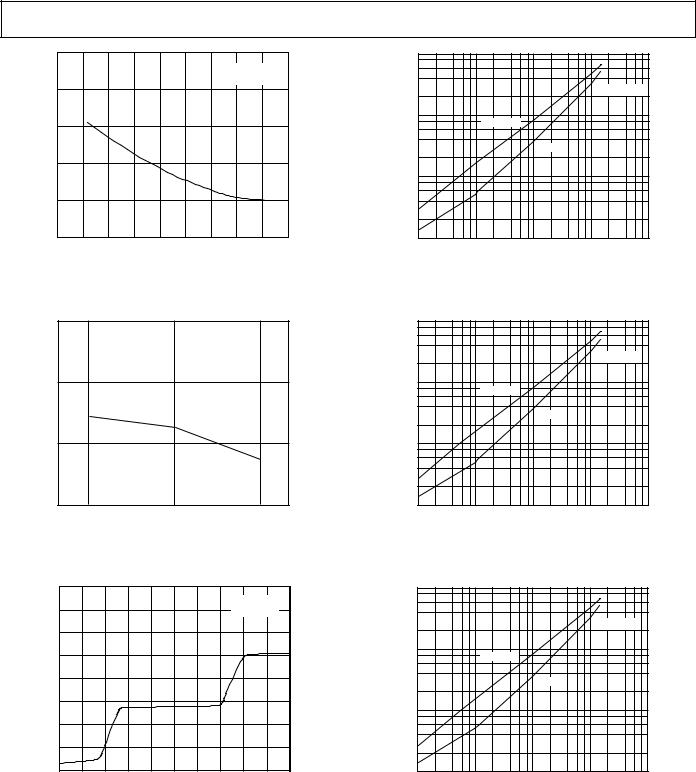
TPC 4. Input Offset Voltage Distribution (TCVOS)
|
25 |
|
|
|
|
|
|
|
|
|
|
|
|
|
|
|
|
|
V |
S = 12V |
|||
|
|
|
VCM = 6V |
||||
Amplifiers– |
20 |
|
TA = –40 C TO 125 C |
||||
|
|||||||
15 |
|
|
|
|
|
|
|
QUANTITY |
|
|
|
|
|
|
|
10 |
|
|
|
|
|
|
|
|
|
|
|
|
|
|
|
|
5 |
|
|
|
|
|
|
|
|
|
|
|
|
|
|
0
–4.0 –3.5 –3.0 –2.5 –2.0 –1.5 –1.0 –0.5 0 0.5 1.0 1.5 INPUT OFFSET DRIFT, TCVOS – V/ C
TPC 5. Input Offset Voltage Distribution (TCVOS)
QUANTITY – Amplifiers
250 |
|
|
|
|
|
|
|
|
|
|
|
|
|
|
|
|
|
|
|
|
|
|
|
|
|
|
|
|
|
|
|
|
|
|
|
|
|
|
|
|
|
|
|
|
|
|
|
|
|
|
|
|
|
|
|
|
|
|
VS |
= 12V |
|
|
|||
200 |
|
|
|
|
|
|
|
|
|
|
|
|
|
|
TA = 25 C |
|
|
|
|||
|
|
|
|
|
|
|
|
|
|
|
|
|
|
|
|
|
|||||
|
|
|
|
|
|
|
|
|
|
|
|
|
|
|
COUNT = 400 |
|
|
|
|||
150 |
|
|
|
|
|
|
|
|
|
|
|
|
|
|
|
|
|
|
|
|
|
|
|
|
|
|
|
|
|
|
|
|
|
|
|
|
|
|
|
|
|
|
|
|
|
|
|
|
|
|
|
|
|
|
|
|
|
|
|
|
|
|
|
|
|
100 |
|
|
|
|
|
|
|
|
|
|
|
|
|
|
|
|
|
|
|
|
|
|
|
|
|
|
|
|
|
|
|
|
|
|
|
|
|
|
|
|
|
|
|
50 |
|
|
|
|
|
|
|
|
|
|
|
|
|
|
|
|
|
|
|
|
|
|
|
|
|
|
|
|
|
|
|
|
|
|
|
|
|
|
|
|
|
|
|
|
|
|
|
|
|
|
|
|
|
|
|
|
|
|
|
|
|
|
|
|
|
0 |
|
|
|
|
|
|
|
|
|
|
|
|
|
|
|
|
|
|
|
|
|
|
|
|
|
|
|
|
|
|
|
|
|
|
|
|
|
|
|
|
|
|
|
|
|
|
|
|
|
|
|
|
|
|
|
|
|
|
|
|
|
|
|
|
|
–250 –200 –150 –100 –50 |
0 |
50 100 150 200 250 |
|||||||||||||||||||
INPUT OFFSET VOLTAGE – V
|
600 |
|
|
|
|
|
|
|
|
|
|
400 |
|
|
|
|
3V |
VS |
12V |
|
|
V |
|
|
|
|
|
VS |
|
|
|
|
|
|
|
|
|
|
|
|
|
||
|
|
|
|
|
VCM = 2 |
|
|
|
||
– |
|
|
|
|
|
|
|
|
|
|
VOLTAGE |
200 |
|
|
|
|
|
|
|
|
|
|
|
|
|
|
|
|
|
|
|
|
OFFSET |
0 |
|
|
|
|
|
|
|
|
|
|
|
|
|
|
|
|
|
|
|
|
INPUT |
–200 |
|
|
|
|
|
|
|
|
|
|
|
|
|
|
|
|
|
|
|
|
|
–400 |
–50 |
–25 |
0 |
25 |
50 |
75 |
100 |
125 |
150 |
|
–75 |
|||||||||
|
|
|
|
|
TEMPERATURE – C |
|
|
|
||
TPC 3. Input Offset Voltage Distribution |
TPC 6. Input Offset Voltage vs. Temperature |
–6– |
REV. C |
|
|
|
|
|
|
|
|
|
|
|
|
|
|
OP196/OP296/OP496 |
||
|
25 |
|
|
|
|
|
|
|
|
|
|
1000 |
|
|
|
|
|
|
|
|
|
|
|
|
VS = 5V |
|
|
|
|
|
|
|
|
|
|
|
|
|
|
|
|
VCM = 2.5V |
|
|
|
|
|
|
VS = 1.5V |
|
|
20 |
|
|
|
|
|
|
|
|
|
|
|
|
|
|
|
– nA |
|
|
|
|
|
|
|
|
|
|
– mV |
100 |
|
|
|
|
CURRENT |
|
|
|
|
|
|
|
|
|
|
VOLTAGE |
SOURCE |
|
|
||
15 |
|
|
|
|
|
|
|
|
|
|
|
|
||||
|
|
|
|
|
|
|
|
|
|
|
|
|
|
|||
|
|
|
|
|
|
|
|
|
|
|
|
|
|
|
|
|
INPUTBAIS |
|
|
|
|
|
|
|
|
|
|
OUTPUT |
|
|
SINK |
|
|
5 |
|
|
|
|
|
|
|
|
|
|
|
|
|
|
||
|
10 |
|
|
|
|
|
|
|
|
|
|
|
|
|
|
|
|
|
|
|
|
|
|
|
|
|
|
|
10 |
|
|
|
|
|
0 |
–50 |
–25 |
0 |
25 |
50 |
75 |
100 |
125 |
150 |
|
1 |
|
|
|
|
|
–75 |
|
0.001 |
0.01 |
0.1 |
1 |
10 |
|||||||||
|
|
|
|
|
TEMPERATURE – C |
|
|
|
|
|||||||
|
|
|
|
|
|
|
|
|
|
|
LOAD CURRENT – mA |
|
|
|||
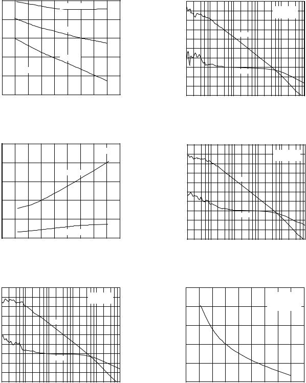
TPC 7. Input Bias Current vs. Temperature
|
16 |
|
– nA |
12 |
|
BIAS CURRENT |
||
8 |
||
INPUT |
||
|
4
2 |
3 |
5 |
12 |
14 |
SUPPLY VOLTAGE – V
TPC 8. Input Bias Current vs. Supply Voltage
|
40 |
|
|
|
|
|
|
|
|
|
|
|
30 |
|
|
|
|
|
|
|
VS = 2.5V |
|
|
|
|
|
|
|
|
|
|
TA = 25 C |
|
||
nA |
20 |
|
|
|
|
|
|
|
|
|
|
– |
|
|
|
|
|
|
|
|
|
|
|
BIAS CURRENT |
10 |
|
|
|
|
|
|
|
|
|
|
0 |
|
|
|
|
|
|
|
|
|
|
|
–10 |
|
|
|
|
|
|
|
|
|
|
|
INPUT |
–20 |
|
|
|
|
|
|
|
|
|
|
|
|
|
|
|
|
|
|
|
|
|
|
|
–30 |
|
|
|
|
|
|
|
|
|
|
|
–40 |
|
|
|
|
|
|
|
|
|
|
|
–2.5 |
–2.0 |
–1.5 |
–1.0 |
–0.5 |
0 |
0.5 |
1.0 |
1.5 |
2.0 |
2.5 |
COMMON-MODE VOLTAGE – V
TPC 10. Output Voltage to Supply Rail vs. Load Current
|
1000 |
|
|
|
|
|
|
|
|
|
VS = 2.5V |
– mV |
100 |
|
|
|
|
VOLTAGE |
SOURCE |
|
|
|
|
|
|
|
|
||
|
|
SINK |
|
|
|
|
|
|
|
|
|
OUTPUT |
10 |
|
|
|
|
|
|
|
|
|
|
|
1 |
|
|
|
|
|
0.001 |
0.01 |
0.1 |
1 |
10 |
LOAD CURRENT – mA
TPC 11. Output Voltage to Supply Rail vs. Load Current
|
1000 |
|
|
|
|
|
|
|
|
|
VS = 6V |
– mV |
100 |
|
|
|
|
VOLTAGE |
SOURCE |
|
|
||
|
|
|
|||
|
|
SINK |
|
|
|
|
|
|
|
|
|
OUTPUT |
10 |
|
|
|
|
|
|
|
|
|
|
|
1 |
|
|
|
|
|
0.001 |
0.01 |
0.1 |
1 |
10 |
|
|
|
LOAD CURRENT – mA |
|
|
TPC 9. Input Bias Current vs. Common-Mode Voltage |
TPC 12. Output Voltage to Supply Rail vs. Load Current |
REV. C |
–7– |
OP196/OP296/OP496 |
|
|
|
|
|
|||||
|
4.95 |
|
|
|
|
IL = 100 A |
|
|
|
|
|
|
|
|
|
|
|
|
|
||
|
4.70 |
|
|
|
|
|
|
|
|
|
– V |
|
|
|
|
|
IL = 1mA |
|
|
|
|
VOLTAGE |
|
|
|
|
|
|
|
|
|
|
4.45 |
|
|
|
|
|
|
|
|
|
|
|
|
|
|
|
|
|
|
|
|
|
OUTPUT |
4.2 |
|
|
|
|
IL = 2mA |
|
|
|
|
|
|
VS = 5V |
|
|
|
|
|
|
|
|
OH |
|
|
|
|
|
|
|
|
|
|
|
|
|
|
|
|
|
|
|
|
|
V |
3.85 |
|
|
|
|
|
|
|
|
|
|
|
|
|
|
|
|
|
|
|
|
|
3.7 |
–50 |
–25 |
0 |
25 |
50 |
75 |
100 |
125 |
150 |
|
–75 |
|||||||||
|
|
|
|
|
TEMPERATURE – C |
|
|
|
||
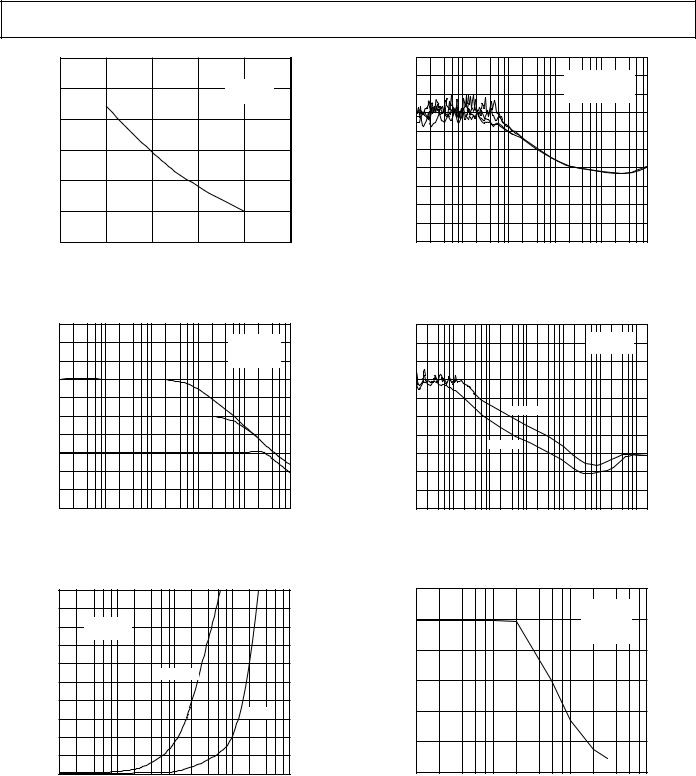
TPC 13. Output Voltage Swing vs. Temperature
|
0.80 |
|
|
|
|
|
|
|
|
|
|
|
|
|
|
|
|
|
VS = 5V |
|
|
– V |
0.60 |
|
|
|
|
|
|
|
|
|
|
|
|
|
|
IL = –1mA |
|
|
|
||
VOLTAGE |
|
|
|
|
|
|
|
|
||
0.50 |
|
|
|
|
|
|
|
|
|
|
|
|
|
|
|
|
|
|
|
|
|
OUTPUT |
0.30 |
|
|
|
|
|
|
|
|
|
|
|
|
|
|
|
|
|
|
|
|
OL |
|
|
|
|
|
|
|
|
|
|
V |
0.10 |
|
|
|
|
|
|
|
|
|
|
|
|
|
|
|
|
|
|
|
|
|
|
|
|
|
|
IL = –100 A |
|
|
|
|
|
–75 |
–50 |
–25 |
0 |
25 |
50 |
75 |
100 |
125 |
150 |
|
|
|
|
|
TEMPERATURE – C |
|
|
|
||
TPC 14. Output Voltage Swing vs. Temperature
|
90 |
|
|
|
|
|
|
|
80 |
|
|
|
VS = 2.5V |
|
|
|
|
|
|
|
TA = 25 C |
|
|
|
70 |
|
|
|
|
|
|
dB |
60 |
|
GAIN |
|
|
|
|
– |
|
|
|
|
|
|
|
GAIN |
50 |
|
|
|
|
|
|
|
|
|
|
|
|
||
40 |
|
|
|
|
0 |
|
|
OPEN-LOOP |
|
|
|
|
|
||
30 |
|
|
|
|
45 |
SHIFT – C |
|
20 |
|
PHASE |
|
|
90 |
||
|
|
|
|
|
|||
10 |
|
|
|
|
135 |
||
|
|
|
|
|
PHASE |
||
|
0 |
|
|
|
|
180 |
|
|
|
|
|
|
|
|
|
|
–10 |
100 |
1k |
10k |
100k |
225 |
|
|
10 |
1M |
|
||||
|
|
|
FREQUENCY – Hz |
|
|
|
|
TPC 15. Open-Loop Gain and Phase vs. Frequency (No Load)
|
90 |
|
|
|
|
|
|
|
80 |
|
|
|
VS = 2.5V |
|
|
|
|
|
|
|
TA = –40 C |
|
|
|
70 |
|
|
|
|
|
|
– dB |
60 |
|
GAIN |
|
|
|
|
|
|
|
|
|
|
||
GAIN |
50 |
|
|
|
|
|
|
40 |
|
|
|
|
0 |
|
|
OPEN-LOOP |
|
|
|
|
|
||
30 |
|
|
|
|
45 |
SHIFT – C |
|
20 |
|
PHASE |
|
|
90 |
||
|
|
|
|
|
|||
10 |
|
|
|
|
135 |
||
|
|
|
|
|
PHASE |
||
|
0 |
|
|
|
|
180 |
|
|
|
|
|
|
|
|
|
|
–10 |
100 |
1k |
10k |
100k |
225 |
|
|
10 |
1M |
|
||||
|
|
|
FREQUENCY – Hz |
|
|
|
|
TPC 16. Open-Loop Gain and Phase vs. Frequency (No Load)
|
90 |
|
|
|
|
|
|
|
80 |
|
|
|
VS = 2.5V |
|
|
|
|
|
|
|
TA = 125 C |
|
|
|
70 |
|
|
|
|
|
|
dB |
60 |
|
|
|
|
|
|
– |
|
|
|
GAIN |
|
|
|
GAIN |
50 |
|
|
|
|
|
|
|
|
|
|
|
|
||
40 |
|
|
|
|
0 |
|
|
OPEN-LOOP |
|
|
|
|
|
||
30 |
|
|
|
|
45 |
SHIFT – C |
|
20 |
|
|
PHASE |
|
90 |
||
|
|
|
|
|
|||
10 |
|
|
|
|
135 |
||
|
|
|
|
|
PHASE |
||
|
0 |
|
|
|
|
180 |
|
|
|
|
|
|
|
|
|
|
–10 |
100 |
1k |
10k |
100k |
225 |
|
|
10 |
1M |
|
FREQUENCY – Hz
TPC 17. Open-Loop Gain and Phase vs. Frequency (No Load)
|
950 |
|
|
|
|
|
|
|
|
|
|
|
|
|
|
|
|
|
VS = 5V |
|
|
|
|
|
|
|
|
|
|
0.3V < VO < 4.7V |
|
|
|
800 |
|
|
|
|
|
|
RL = 100k |
|
|
V/mV |
650 |
|
|
|
|
|
|
|
|
|
GAIN – |
|
|
|
|
|
|
|
|
|
|
|
|
|
|
|
|
|
|
|
|
|
OPEN-LOOP |
500 |
|
|
|
|
|
|
|
|
|
350 |
|
|
|
|
|
|
|
|
|
|
|
|
|
|
|
|
|
|
|
|
|
|
200 |
–50 |
–25 |
0 |
25 |
50 |
75 |
100 |
125 |
150 |
|
–75 |
|||||||||
|
|
|
|
|
TEMPERATURE – C |
|
|
|
||
TPC 18. Open-Loop Gain vs. Temperature
–8– |
REV. C |
|
|
|
|
|
|
|
|
|
|
OP196/OP296/OP496 |
|||
|
600 |
|
|
|
|
|
|
160 |
|
|
|
|
|
|
|
|
|
|
VS = 5V |
|
|
140 |
|
|
VS = 2.5V |
|
|
|
500 |
|
|
|
|
|
|
|
|
T |
= 25 C |
|
|
|
|
|
|
TA = 25 C |
|
|
120 |
|
|
A |
|
|
|
V/mV |
|
|
|
|
|
|
|
|
ALL CHANNELS |
|
|||
400 |
|
|
|
|
|
|
100 |
|
|
|
|
|
|
|
|
|
|
|
|
|
|
|
|
|
|
|
|
– |
|
|
|
|
|
|
|
80 |
|
|
|
|
|
GAIN |
|
|
|
|
|
|
– dB |
|
|
|
|
|
|
300 |
|
|
|
|
|
60 |
|
|
|
|
|
||
LOOP-OPEN |
|
|
|
|
|
CMRR |
|
|
|
|
|
||
|
|
|
|
|
|
40 |
|
|
|
|
|
||
|
|
|
|
|
|
|
|
|
|
|
|
|
|
|
200 |
|
|
|
|
|
|
20 |
|
|
|
|
|
|
|
|
|
|
|
|
|
|
|
|
|
|
|
|
100 |
|
|
|
|
|
|
0 |
|
|
|
|
|
|
|
|
|
|
|
|
|
|
|
|
|
|
|
|
|
|
|
|
|
|
|
–20 |
|
|
|
|
|
|
0 |
100 |
50 |
10 |
2 |
1 |
|
–40 |
1k |
10k |
100k |
1M |
10M |
|
150 |
|
100 |
||||||||||
|
|
|
|
LOAD – k |
|
|
|
|
|
FREQUENCY – Hz |
|
|
|
TPC 19. Open-Loop Gain vs. Resistive Load
|
70 |
|
|
|
|
|
|
60 |
|
|
|
VS = 2.5V |
|
|
|
|
|
|
RL = 10k |
|
|
50 |
|
|
|
TA = 25 C |
|
dB |
40 |
|
|
|
|
|
– |
|
|
|
|
|
|
|
|
|
|
|
|
|
GAIN |
30 |
|
|
|
|
|
|
|
|
|
|
|
|
CLOSED-LOOP |
20 |
|
|
|
|
|
10 |
|
|
|
|
|
|
0 |
|
|
|
|
|
|
–10 |
|
|
|
|
|
|
|
|
|
|
|
|
|
|
–20 |
|
|
|
|
|
|
–30 |
100 |
1k |
10k |
100k |
1M |
|
10 |
FREQUENCY – Hz
TPC 20. Closed-Loop Gain vs. Frequency
|
1000 |
|
|
|
|
|
900 |
|
|
|
|
|
800 |
VS = 2.5V |
|
|
|
|
TA = 25 C |
|
|
|
|
– |
|
|
|
|
|
IMPEDANCE |
700 |
|
|
|
|
600 |
|
ACL = 10 |
|
|
|
500 |
|
|
|
||
|
|
|
|
||
|
|
|
|
|
|
OUTPUT |
400 |
|
|
|
|
300 |
|
|
|
ACL = 1 |
|
|
|
|
|
||
|
|
|
|
|
|
|
200 |
|
|
|
|
|
100 |
|
|
|
|
|
0 |
|
|
|
|
|
100 |
1k |
10k |
100k |
1M |
|
|
|
FREQUENCY – Hz |
|
|
TPC 21. Output Impedance vs. Frequency
TPC 22. CMRR vs. Frequency
|
160 |
|
|
|
|
|
|
|
140 |
|
|
|
|
VS = 5V |
|
|
|
|
|
|
TA = 25 C |
|
|
|
|
|
|
|
|
|
|
|
120 |
|
|
|
|
|
|
|
100 |
|
|
|
|
|
|
dB |
80 |
|
|
|
|
|
|
– |
|
|
|
+PSRR |
|
|
|
PSRR |
60 |
|
|
|
|
|
|
|
|
|
|
|
|
||
40 |
|
|
|
|
|
|
|
|
|
–PSRR |
|
|
|
||
|
|
|
|
|
|
||
|
20 |
|
|
|
|
|
|
|
0 |
|
|
|
|
|
|
|
–20 |
|
|
|
|
|
|
|
–40 |
100 |
1k |
10k |
100k |
1M |
10M |
|
10 |
||||||
|
|
|
|
FREQUENCY – Hz |
|
|
|
TPC 23. PSRR vs. Frequency
|
6 |
|
|
|
|
|
|
|
VS = 2.5V |
|
5 |
|
|
VIN = 5V p-p |
V |
|
|
|
AV = 1 |
– |
|
|
|
RL = 100k |
SWING |
|
|
|
|
4 |
|
|
|
|
|
|
|
|
|
OUTPUT |
3 |
|
|
|
|
|
|
|
|
MAXIMUM |
2 |
|
|
|
1 |
|
|
|
|
|
|
|
|
|
|
0 |
|
|
|
|
1k |
10k |
100k |
1M |
|
|
|
FREQUENCY – Hz |
|
TPC 24. Maximum Output Swing vs. Frequency
REV. C |
–9– |
OP196/OP296/OP496 |
|
|
|
|
|
|
||||
|
90 |
|
|
|
|
|
|
|
|
|
|
80 |
|
|
|
|
|
|
|
|
|
A |
70 |
|
|
|
|
|
|
|
|
|
|
|
|
|
VS = 12V |
|
|
|
|||
– |
|
|
|
|
|
|
|
|||
/AMPLIFIER |
60 |
|
|
|
|
|
|
|||
|
|
|
|
|
|
|
|
|
||
50 |
|
|
|
|
|
|
|
|
|
|
|
|
|
|
|
|
|
|
|
|
|
SY |
|
|
|
|
V |
= 5V |
|
|
|
|
I |
40 |
|
|
|
S |
|
|
|
|
|
|
|
|
|
|
|
|
|
|
|
|
|
30 |
|
|
VS = 3V |
|
|
|
|
|
|
|
|
|
|
|
|
|
|
|
|
|
|
20 |
|
|
|
|
|
|
|
|
|
|
–75 |
–50 |
–40 –25 |
0 25 |
50 |
75 |
85 |
100 |
125 |
150 |
|
|
|
|
TEMPERATURE – C |
|
|
|
|
||
TPC 25. Supply Current/Amplifier vs. Temperature
|
55 |
|
|
|
|
|
|
|
|
|
|
|
|
|
TA = 25 C |
|
|
|
50 |
|
|
|
|
|
|
|
A |
|
|
|
|
|
|
|
|
– |
|
|
|
|
|
|
|
|
/AMPLIFIER |
45 |
|
|
|
|
|
|
|
|
|
|
|
|
|
|
|
|
SY 40 |
|
|
|
|
|
|
|
|
I |
|
|
|
|
|
|
|
|
|
35 |
3 |
5 |
7 |
9 |
11 |
12 |
13 |
|
1 |
|||||||
SUPPLY VOLTAGE – V
TPC 26. Supply Current/Amplifier vs. Supply Voltage
|
80 |
|
|
|
|
70 |
|
|
VS = 2.5V |
Hz |
|
|
TA = 25 C |
|
|
|
|
VCM = 0V |
|
– nV/ |
60 |
|
|
|
DENSITY |
40 |
|
|
|
|
50 |
|
|
|
NOISE |
30 |
|
|
|
VOLTAGE |
10 |
|
|
|
|
20 |
|
|
|
|
0 |
10 |
100 |
1k |
|
1 |
|||
|
|
|
FREQUENCY – Hz |
|
TPC 27. Voltage Noise Density vs. Frequency
|
0.6 |
|
|
|
|
|
|
|
VS = 2.5V |
Hz |
0.5 |
|
|
TA = 25 C |
|
|
|
VCM = 0V |
|
– pA/ |
0.4 |
|
|
|
DENSITY |
0.3 |
|
|
|
|
|
|
|
|
NOISE |
0.2 |
|
|
|
CURRENT |
0.1 |
|
|
|
|
|
|
|
|
|
0 |
10 |
100 |
1k |
|
1 |
FREQUENCY – Hz
TPC 28. Input Bias Current Noise Density vs. Frequency
|
10 |
|
|
|
|
|
|
|
8 |
VS = 6V |
|
|
|
|
|
|
6 |
TA = 25 C |
|
|
|
|
|
|
TO 0.1% |
|
OUTPUT SWING |
|
|
||
|
|
|
|
|
|||
|
|
|
|
|
|
||
|
4 |
|
|
|
|
|
|
V |
2 |
|
|
|
|
|
|
– |
|
|
|
|
|
|
|
STEP |
0 |
|
|
|
|
|
|
INPUT |
–2 |
|
|
|
|
|
|
|
|
|
|
|
|
|
|
|
–4 |
|
|
|
– OUTPUT SWING |
|
|
|
|
|
|
|
|
||
|
–6 |
|
|
|
|
|
|
|
–8 |
|
|
|
|
|
|
|
–10 |
5 |
10 |
15 |
20 |
25 |
30 |
|
0 |
||||||
|
|
|
SETTLING TIME – s |
|
|
||
TPC 29. Settling Time to 0.1% vs. Step Size
|
2mV |
1s |
100 |
|
|
90 |
|
|
10 |
VS = 2.5V |
|
0% |
AV = 10k |
|
|
|
|
|
en = 0.8 V p-p |
|
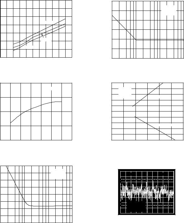
TPC 30. 0.1 Hz to 10 Hz Noise
–10– |
REV. C |