

Книги+1 / 2013 [Chandan_Kumar_Sarkar]_Technology_CAD
.pdfBasic Semiconductor and Metal-Oxide-Semiconductor (MOS) Physics |
103 |
The flat-band voltage in Equation (2.105) must be added to the expression of the threshold voltage in (2.107), in order to accurately describe the actual, “non-ideal” threshold voltage given as
VTH = VFB + 2ΦF − |
Qd |
= Φms − |
Qit |
+ 2ΦF − |
Qd |
(2.108) |
|
COX |
COX |
COX |
|||||
|
|
|
|
For strong inversion the voltage required must be strong enough to first achieve the flat band condition (first two terms of Equation 2.108), then to induce an inverted region (2ΦF term of Equation 2.108) and to accommodate the charge in the depletion region (last term of Equation 2.108).
The threshold voltage may be either positive or negative, depending on the doping concentration Na, the material used to form the gate electrode, etc. If the threshold voltage is negative, the n-channel MOSFET is a depletion-mode device. However, if VTH 0 is positive, the device is an enhancement-mode MOSFET.
Depletion-mode devices have an inversion layer when the gate voltage is equal to zero. Such devices are sometimes referred to as “normally on.” Enhancement-mode devices called “normally off” require an applied positive gate bias to create the inversion layer. The value of the threshold voltage can be adjusted by applying a controlled amount of doping impurities in the channel region during device fabrication.
2.17 I–V Characteristics of MOSFET
The derivation of the MOSFET I–V relationship for different conditions needs several approximations. The analysis of an actual three-dimensional MOSFET would be a very complex task without these assumptions. Derivation of closed form I–V equations is not possible without these assumptions. Here gradual channel approximation (GCA) is used for deriving the I–V relationship, which will effectively reduce the problem to a one-dimensional current flow problem. This will allow us to devise simple current equations that are in agreement with experimental results. However, GCA has limitations, particularly in the case of short-channel MOSFETs.
2.17.1 Gradual Channel Approximation
A semiconductor bar carrying a current I is considered in Figure 2.36. If Qd coulombs per meter is the density of charge along the direction of current and v meters per second is the velocity of the charge, then
I = Qdv |
(2.109) |
The total charge that passes through a cross section of the bar per unit time can be measured. With a velocity v, the charge enclosed in v meters of the bar must
104 |
Technology Computer Aided Design: Simulation for VLSI MOSFET |
I
V meters
After one second
FIGURE 2.36
A semiconductor bar carrying current and snaps of the carriers after 1 second.
flow through the cross section in one second. Because the charge density is Qd, the total charge in ‘v’ meters is given by Qdv.
In Figure 2.37(a) a coordinate system for the MOSFET structure is considered taking the x-direction parallel to the surface and the y-direction perpendicular to the surface. The origin of the x-coordinate is at the source end of the channel. The channel voltage with respect to the source end is denoted by V(x). Now let the threshold voltage Vth be constant along the entire channel region between x = 0 and x = L. However, in reality the threshold voltage changes along the channel because the channel voltage is not constant. Let the electric field component Ex along x-coordinate be dominant compared to electric field component EY along the y-coordinate. This allows us to reduce the current flow problem in the channel along the x-direction only.
Boundary conditions used are
V(x=0) = VS = 0 |
(2.110) |
V(x=L) = VDS |
(2.111) |
Basic Semiconductor and Metal-Oxide-Semiconductor (MOS) Physics |
105 |
Source
n+
p-type substrate
(a)
Source
n+
p-type substrate
(b)
FIGURE 2.37
+ –
VGS
Gate
x = 0 |
L |
y |
|
|
Body |
+ |
VGS |
– |
Gate
x = 0 |
L |
y |
|
|
Body |
Drain
VGS + –
n+
x
VDS
Drain + –
VGS
+ –
n+
+ –
VDS
x
(a) Channel charge with equal source and drain voltages and (b) with only drain voltage.
Let an n-channel MOSFET whose source and drain are connected to ground be considered. When VGS = VTH, the inversion charge density produced by the gate oxide capacitance is proportional to VGS – VTH. For VGS ≥ VTH, any charge placed on the gate must be mirrored by the charge in the channel, yielding a uniform channel charge density equal to
Qd = COXW(VGS − VTH ) |
(2.112) |
COX is the gate/channel capacitance per unit area, where COX is multiplied by W to represent total gate capacitance per unit length. Sometimes
106 |
Technology Computer Aided Design: Simulation for VLSI MOSFET |
expressions are described in terms of another capacitance known as gate/ channel capacitance Cg.
Cg = COXWL |
(2.113) |
Now let the drain voltage taken be greater than zero as shown in Figure 2.37(b). Because the channel potential varies from zero at the source end to VD at the drain, the potential difference between the gate and the channel varies from VG to VG – VD. Thus the charge density at a point x along the channel can be written as
Qd (x) = COXW[(VGS − V(x) − VTH ] |
(2.114) |
where V(x) is the channel potential at x. The drain current is given by
ID = −COXW[(VGS − V(x) − VTH ]v |
(2.115) |
In this expression the negative are negative and v denotes the semiconductors v = μE, where
–dV/dx is the electric field. Putting the value of v
sign is inserted because the charge carriers velocity of the electrons in the channel. For μ is the mobility of charge carriers and E =
ID = COXW[(VGS − V(x) − VTH ]µn dV(x) |
(2.116) |
dx |
|
The boundary conditions are V(0) = 0 and V(L) = VDS. Although V(x) can easily be found from this equation, the quantity of interest is ID . Integrating (2.116) we get
∫L |
ID dx = V∫DS WCOXµn[VGS − V(x) − VTH ]dV |
(2.117) |
x=0 |
V=0 |
|
The current equation of MOSFET in the triode region is given by
ID = µnCOX |
W |
[(VGS − VTH )VDS − |
1 |
VDS2 |
] |
(2.118) |
|
L |
2 |
||||||
|
|
|
|
|
where L is the effective channel length.
Figure 2.38 plots the parabolas given by Equation (2.118) for different values of VGS. Calculating ∂ID/∂VGS, one can show that the peak of each parabola occurs at VDS = VGS – VTH, and the peak current is
ID,max = |
1 |
µnCOX |
W |
(VGS − VTH )2 |
(2.119) |
|
2 |
L |
|||||
|
|
|
|
Basic Semiconductor and Metal-Oxide-Semiconductor (MOS) Physics |
107 |
Drain Current ID
VGS3
VGS2
VGS1
th |
th |
th |
– V |
– V |
– V |
GS1 |
GS2 |
GS3 |
V V V |
||
FIGURE 2.38
Drain Voltage VDS
Drain current versus drain-source voltage in triode region.
Here, (VGS – VTH) is the overdrive or effective voltage and W/L is the aspect ratio. If VDS ≤ VGS – VTH, we say the device is operating in the triode or linear region.
kn′ = nCOX is known as the process transconductance parameter.
kn = WL kn′ = WL µnCOX is known as the gain factor.
Equations (2.118) and (2.119) serve as the foundation for analog and digital CMOS VLSI design.
If in (2.118) VDS < 2(VG S– VTH), we have
ID ≈ µnCOX |
W |
[(VGS − VTH )VDS ] |
(2.120) |
|
L |
|
|
The drain current is a linear function of VDS. This is also evident from the characteristics of Figure 2.38. For small VDS, each parabola can be approximated by a straight line. The linear relationship implies that the path from the source to the drain can be approximated by a linear resistor equal to
Ron = |
1 |
(2.121) |
µnCOX WL (VGS − VTH ) |
108 |
Technology Computer Aided Design: Simulation for VLSI MOSFET |
VGS3
ID
VGS2 |
|
VGS1 |
Approximate linear |
|
operation in deep |
|
triode region |
VDS |
|
FIGURE 2.39
Linear operation in deep triode region.
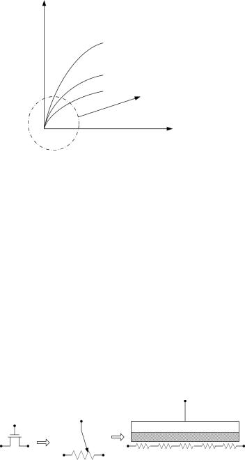
A MOSFET can therefore operate as a resistor whose value is controlled by the overdrive voltage (as long as VDS < 2(VGS – VTH)). This is shown in Figure 2.39. Thus in triode region, MOSFET operates as a voltage controlled resistor as in Figure 2.40.
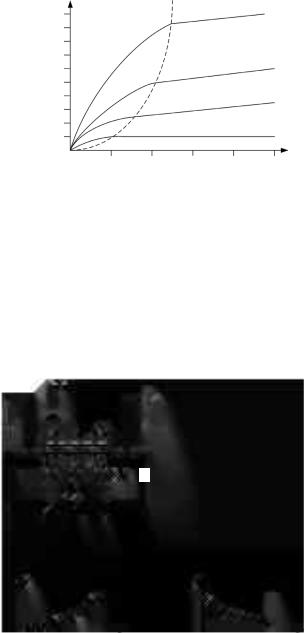
However, if in Figure 2.38 the drain-source voltage exceeds VGS – VTH, the drain current does not follow the parabolic behavior for VDS > VGS – VTH. In fact, as shown in Figure 2.41, ID becomes relatively constant, and we say that the device operates in the saturation region as in [38,41].
If the drain voltage remains greater than the source voltage, then the voltage at each point along the channel with respect to ground increases as we move from the source end toward the drain end. From Figure 2.42(a), this effect arises from the gradual voltage drop along the channel resistance. Because the gate voltage is constant (as the gate is conductive but carries no current in any direction) and the potential at the oxide-silicon interface rises from the source to the drain end, the potential difference between the gate
|
|
|
Gate |
Gate |
|
Gate |
|
Source |
Drain |
Source |
Drain |
|
Source |
Drain |
|
FIGURE 2.40
MOSFET as a voltage-dependent resistor.
Basic Semiconductor and Metal-Oxide-Semiconductor (MOS) Physics |
109 |
||||
|
VDS(sat) = VGS – Vth |
|
|
||
500 µA |
|
|
VGS = 3.25 V |
|
|
|
|
|
|
|
|
400 µA |
|
Saturation region |
|
|
|
ID 300 µA |
Triode |
|
VGS = 2.75 V |
|
|
region |
|
|
|
|
|
|
|
|
|
|
|
200 µA |
|
|
VGS = 2.3 V |
|
|
100 µA |
|
VGS = 0.45 V(Cuto region) |
|
||
|
|
|
|||
1 |
2 |
3 |
4 |
5 |
|
|
|
VDS in (V) |
|
|
|
FIGURE 2.41
Plots showing saturation of drain current.
and the oxide-silicon interface decreases along the x-axis as in Figure 2.42(b). The density of electrons in the channel follows the same trend, falling to a minimum value at x = L.
The local density of inversion layer charge is proportional to VGS −V(x) −VTH .
So if V(x) approaches VGS −VTH, then Qd (x) drops to zero. In other words, as in Figure 2.43(a), if VDS is slightly greater than VGS −VTH, then the inversion
VG |
VD |
– + |
|
|
+ – |
n+ |
|
|
n+ |
|
|
|
|
|
ID |
X- |
direction |
|
|
|
|
|
|
|
|
|
Potential |
= VG |
<VG |
= VG – VD |
|
|
|
di erence |
|
|
||||
V(x) |
|
|
|
VG |
Gate to body potential |
|
|
|
|
|
|
||
|
|
|
|
|
drop |
|
|
|
|
|
VG – VD |
|
|
|
(a) |
L |
x |
L |
x |
|
|
|
|
|
(b) |
|
|
FIGURE 2.42
(a) Channel potential variation. (b) Gate-substrate voltage difference along the channel.
110 |
Technology Computer Aided Design: Simulation for VLSI MOSFET |
S
n+
p-type substrate
(a)
S
n+
p-type substrate
(b)
FIGURE 2.43
VGS
+ –
G
Pinch o
V(L) = VGS – Vth
x = 0 L
y
Body
VGS
+–
G
Pinch o
x = 0 L1 L
y V(L1) = VGS – Vth
Body
VDS
+1 –
D
n+
X-direction
VDS2 > VDS1
+–
D
n+
X-direction
(a) Pinch-off condition. (b) Pinch-off point shifts to source end for increasing VDS.
layer stops at x ≤ L, and the channel is pinched off. As VDS increases further, as in Figure 2.43(b), the point where Qd equals zero gradually moves toward the source. So at some point along the channel, the local potential difference between the gate and the oxide-silicon interface is not sufficient to support an inversion layer.
No channel exists between L1 and L. But the device still conducts, as illustrated in Figure 2.44. Once the electrons reach the end of the channel, they experience the high electric field in the depletion region at the drain junction and are rapidly swept to the drain terminal.
Basic Semiconductor and Metal-Oxide-Semiconductor (MOS) Physics |
111 |
VG
VS = 0 |
– |
+ |
|
VD |
|
|
|||
|
|
|
+ – |
|
|
|
|
|
ID |
n+ |
|
|
|
n+ |
|
|
|
|
E |
|
0 |
|
L1 L |
x |
|
|
|
FIGURE 2.44
Detailed operation in the pinch-off region.
Drain
n+
From the above observations, we examine (2.117) for a saturated device. The integral on the left-hand side of (2.117) must be taken from x = 0 to x = L1, where L1 is the point at which Qd drops to zero, and that on the right from V(x) = 0 to V(x) = VGS − VTH. As a result,
L∫1 |
ID dx = VGS∫−VTH WCOXµn[VGS − V(x) − VTH ]dV |
|
||||
x=0 |
V=0 |
|
|
|
|
|
which gives |
|
|
|
|
|
|
|
ID,max = |
1 |
µnCOX |
W |
(VGS − VTH )2 |
(2.122) |
|
2 |
|
||||
|
|
|
2L1 |
|
||
Considering the approximation L ≈ L1, a saturated MOSFET can be used as a current source connected between the drain and the source. Current sources draw current from VDD or inject current into ground as shown in Figure 2.45.
|
|
|
VDD |
|
|
|
VDD |
|
I1 |
|
|
VG |
I1 |
VG |
|
|
I2 |
||
|
|
|
|
|
|
|
I2 |
FIGURE 2.45
MOSFET acting as a current source.
112 |
Technology Computer Aided Design: Simulation for VLSI MOSFET |
2.18 Depletion MOSFET
Some devices have an already fabricated channel even at zero gate voltage. Negative gate voltage is required to turn them off [41]. Such a normally on device is known as a depletion-type MOSFET. The MOSFETs that are off at zero gate bias are termed enhancement-type MOSFET. On application of a gate voltage the device turns on.
Figure 2.46 shows an n-channel depletion-type MOSFET. A doped n-chan- nel region exists under the oxide, meaning that an electron inversion layer already exists with zero applied gate bias. In this type of device, a negative gate voltage will induce a space charge region underneath the oxide, reducing the thickness of the n-channel region. The reduced thickness decreases the channel conductance, which in turn, reduces the drain current. A positive gate voltage will create an electron accumulation layer, increasing the drain current. The ID – VDS characteristics and symbol for an n-channel depletion MOSFET are shown in Figures 2.47(a),(b). Figure 2.48 shows the ID – VGS curve for depletion mode and enhancement mode MOSFET.
Source |
Gate |
Drain |
n+ |
n+ |
Ion implanted n-type channel layer
p-type substrate
B
VB = 0
FIGURE 2.46
Structure of a depletion MOSFET.