

Книги+1 / 2013 [Chandan_Kumar_Sarkar]_Technology_CAD
.pdfBasic Semiconductor and Metal-Oxide-Semiconductor (MOS) Physics |
83 |
The above expressions are valid only for minority carriers in a “quasineutral” semiconductor. In steady state the recombination rates of the majority and minority carriers are equal because recombination involves an equal number of holes and electrons. Majority carrier recombination depends on the excess minority carriers.
2.10.4 Impact Ionization Model
Impact ionization is a pure generation process similar to the Auger generation process. When a carrier moves into the conduction or valence band, the energy released is used to move an electron from valence to conduction band causing an electron-hole pair.
The two sub-processes in this case are the electron emission and the hole emission. While in the former a highly energetic electron in conduction band transfers energy to an electron in valence band, in the latter case, a hole in a valence band transfers energy to an electron in the valence band. As a result, the electron from valence band moves to the conduction band. The effect of impact ionization and avalanche multiplication is shown in Figure 2.14.
The current densities for electrons and holes are given as Je and Jh . The generation rates are modeled proportional to these current densities as [9]
ge = |
ie Je |
and gh = |
ih Jh |
(2.84) |
|
q |
q |
||||
|
|
|
where ie and ih are the ionization rates for electrons and holes, respectively. The ionization rates are exponentially dependent on the electric field along
the current flow direction. Let Eelectroncritical and Eholecritical be the critical electric fields for electrons and holes. Let ie∞ and ih∞ be the ionization rates at infinite field
for electrons and holes, respectively. The ionization rates for electrons and holes are given by
i |
= i∞ exp− |
Eelectroncritical |
jelectron |
(2.85) |
|
e |
e |
|
E |
|
|
|
|
|
|
|
|
and |
|
|
|
|
|
|
|
Eholecritical jhole |
|
||
ih = ih∞ exp− |
E |
|
(2.86) |
||
|
|
|
|
|
|
where jelectron and jhole are model parameters with values close to 1.
84 |
Technology Computer Aided Design: Simulation for VLSI MOSFET |
|||||
The total impact ionization rate is now found as |
|
|
|
|||
|
ie Je |
|
ih Jh |
|
||
|
Rtotal,IIR = −(ge + gh ) = − |
|
+ |
|
|
(2.87) |
|
q |
|
||||
|
|
|
q |
|
||
This rate is independent of the electric field but depends on the carrier temperature.
2.10.5 Mobility Modeling
Mobility modeling is divided into four categories: low field mobility, high field mobility, bulk semiconductor mobility, and inversion layer mobility. In low field mobility the carriers are in equilibrium with the lattice and the mobility is very low. This mobility is inversely related to the impurity scattering. The low field mobility models for bulk materials include constant mobility model, Caughey and Thomas model [27], Dorkel-Leturg model [28], Arora model [29], and Klaassen low-field mobility model [30]. The low field mobility is mainly affected by Coulomb scattering. In the high field case the mobility decreases with electric field as the high energy carriers take part in scattering and the mean drift velocity rises slowly with increasing electric field. Finally the drift velocity saturates to a constant value. The bulk mobility model is a three-step process. First the low field mobility is expressed as a function of lattice temperature and doping. Then the saturation velocity is expressed in terms of temperature. And finally the low and high field junction region is described. The mobility models can further be classified into physical based, semiempirical, and empirical models. As carriers move under the influence of an electric field, the velocity saturates and so the effective mobility reduces because the drift velocity is equal to the product of mobility and the electric field. The field-dependent mobility expressions of Caughey and Thomas [27] are
n(E) = n0
p (E) = p0
|
|
|
|
βn − |
1 |
|
|
|
n0E |
βn |
|||||
1 |
+ |
n |
|
|
|
|
|
|
|
vsat |
|
|
|
|
|
|
|
|
|
|
|
|
|
|
|
|
|
βp − |
|
1 |
|
p0E |
|
βp |
|
||||
1 |
+ |
p |
|
|
|
|
|
|
|
vsat |
|
|
|
|
|
|
|
|
|
|
|
|
|
(2.88)
(2.89)
where n0 and p0 are the respective low field electron and hole mobility, and E is the parallel electric field. The saturation velocities are calculated

Basic Semiconductor and Metal-Oxide-Semiconductor (MOS) Physics |
85 |
from the temperature-dependent model in [31] as
p |
n |
24 * 106 |
|
|
|
(2.90) |
|
vsat = vsat = |
|
|
|
|
|||
1 + 0.8exp( |
T |
) cm/sec |
|||||
|
|||||||
|
|
600 |
|
||||
2.11 Introduction to MOS Transistor
The most important requirement for a field-effect transistor (FET) is zero or negligible gate leakage current. It is important to isolate the gate from the channel so that no current flows into the gate. One needs some kind of barrier for the electron (or hole) from the gate to the source, the channel, and the drain. In MOSFET, an insulator provides the barrier. It is possible to grow a high-quality and reliable insulator using Silicon (Si). SiO2 is stable and makes a firm bonding with Silicon. This oxide makes selective diffusion and easy pattern transfer. This has led to the well-established silicon MOSFET technology to become dominant. In MOSFET application of a large gate bias inverts the bands and induces the electrons (or holes) in a channel without the gate leakage. Over the last few years steady progress has been made on using the MOSFET concept with other semiconductors, notably (Gallium Arsenide) GaAs. GaAs n-MOSFETs have channel mobilities much higher than those in n-MOSFET based on the silicon as in [32]. However, GaAs technology does not provide a high-quality oxide. Thus, the widespread use of such devices is still not prevalent because of lack of good-quality oxide.
The Si technology is unique in the sense that a high-quality oxide SiO2 can be formed on the silicon wafer. The Si-SiO2 interface perfection is required for a field-effect device. Their higher areal density, better switching characteristics, and lower power dissipation have made them the dominant device in electronic systems.
There are two basic types of MOS transistors: the n-channel and the p-channel. A circuit containing only n-channel devices is produced by an nMOS process. Similarly, a pMOS process fabricates circuits that contain only p-channel transistors.
2.12 Structure and Symbol of MOSFET
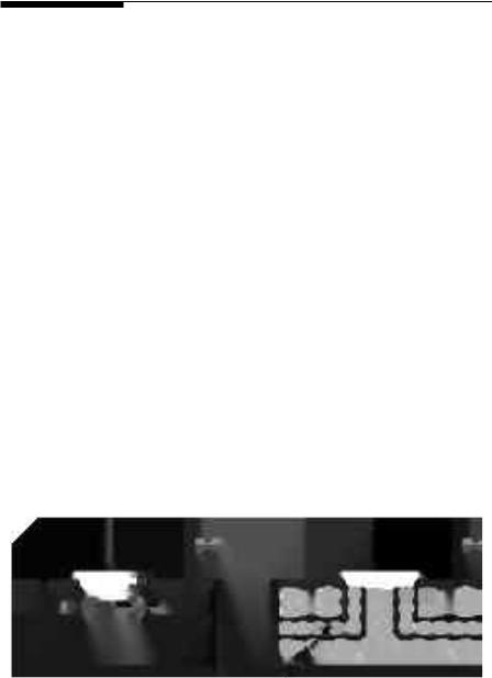
The structure of an n-channel MOS transistor is shown in Figure 2.19(a), consisting of two n-type regions embedded in a p-type substrate, connected via metal or polysilicon to external conductors called the source and the drain.
86 |
Technology Computer Aided Design: Simulation for VLSI MOSFET |
|
|
Source |
Gate |
Drain |
|
|
|
|
|
Conductor |
|
|
|
|
|
plate |
|
|
idth |
W |
|
|
|
W |
|
|
|
D |
|
|
|
|
|
|
|
|
|
|
|
|
G |
|
|
|
|
|
S |
|
|
n+ source |
Oxide |
n+ Drain |
(b) |
|
|
|
|
|
|
|
|
|
thickess tOX |
p type substrate |
|
Insulator oxide |
|
|
|
||
|
|
SiO2 |
Length L |
|
|
(a)
B
FIGURE 2.19
(a) An n-type NMOS device structure. (b) Symbol of MOSFET.
The symbol of MOSFET is shown in Figure 2.19(b). An n-channel MOS transistor is fabricated in a p-type semiconductor substrate, usually silicon [33]. Two n-type regions are made in the substrate and the current flows between these two regions. The region with the lowest applied potential is called the source and that with the highest potential is called the drain. On the surface, a thin silicon dioxide (SiO2) layer is formed and on top of this a conducting polysilicon material called a gate is deposited. An electron-rich layer called a channel can be created between the source and the drain underneath the gate when a positive gate bias is applied. When appropriate voltages are applied at the source and the drain, electrons can flow from the source into the drain. If the substrate material is n-type and the diffused regions are p-type, a similar structure will represent a p-channel MOS transistor. The gate plate must act as a good conductor and was in fact realized by metals like aluminum in the early generations of the MOS technology. However, it was discovered that the non-crystalline polysilicon exhibits better fabrication and physical properties. The bonding between the silicon substrate and polysilicon gate is better than that between the metal gate and the silicon substrate. Thus the metal M is replaced by a heavily doped polysilicon.
Here L and W denote the length and width of the channel, respectively. In the most common mode of operation of the transistor, the source and the substrate are grounded and the drain is connected to a supply voltage VDD through a load resistor, which is positive for an n-channel transistor and negative for a p-channel transistor. In a MOSFET the channel charge is induced electrostatically by the gate by using it as a capacitor without the need for doping.
Basic Semiconductor and Metal-Oxide-Semiconductor (MOS) Physics |
87 |
2.13 Basic Operation of MOSFET
2.13.1 Operation of MOSFET with Zero Gate Voltage
Let us consider the gate voltage equal to zero while the p-type substrate
and the source are grounded (VSub = VS = 0) [34]. The drain is connected to a positive voltage source. Because the source and the substrate are at the
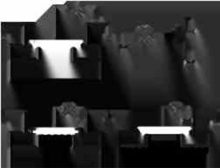
same potential, no current flows in the source-substrate junction. The drainsubstrate junction is reverse biased, and except for a small reverse leakage current, no current flows in that junction. These back-to-back diodes prevent current conduction from the source to the drain, as in Figure 2.20(a). The depletion formation is shown in Figure 2.20(b). The MOSFET has a very high resistance between the source and the drain. It is operating in the “cut off” as there is no conducting channel between the source and the drain. Small current flows due to the second-order effect under the weak inversion, called subthreshold current.
2.13.2 Operation of MOSFET with a Positive Gate Voltage
In this case a constant positive bias is applied to the gate as in Figure 2.21(a). There is no gate current because the metal electrode is insulated from the silicon. However, the positively biased gate electrode attracts electrons from the semiconductor, and an electron-rich layer forms underneath the gate insulator. In effect, negative charges are induced in the underlying Si by the formation of a depletion region and a thin surface region containing mobile electrons.
Source |
Gate |
Drain |
Source |
Gate |
Drain |
n+ |
n+ |
n+ |
p-type bulk si
Depletion layer
(a) nMOS
Operating in cut o mode as VGS < Vth
FIGURE 2.20
(a) Two reverse biased p-n diodes representing a MOSFET MOSFET operating in the “cut-off” mode.
n+
p-type bulk si
(b) Depletion layer formation
working in cutoff regime. (b)
88 |
Technology Computer Aided Design: Simulation for VLSI MOSFET |
+–
Source |
VG |
|
Drain |
|
|
|
|
|
+ |
– |
|
n+ |
|
n+ |
VG |
|
|
|
|
|
|
||
|
p-type |
|
|
|
|
|
substrate |
|
|
|
|
|
(a) |
|
|
|
|
Source |
+ – |
Drain |
Source |
+ – |
Drain |
|
VG |
|
|
VG |
|
n+ |
|
n+ |
n+ |
|
n+ |
|
p-type |
|
|
p-type |
|
|
substrate |
|
|
substrate |
|
|
(b) |
|
|
(c) |
|
FIGURE 2.21
(a) MOSFET with positive gate bias. (b) Formation of depletion region. (c) Formation of channel.
The positive voltage on the gate causes the free holes to be repelled from the region underneath the gate [35]. The holes are pushed downward into the substrate, leaving behind a depletion region. The depletion region is populated by the bound negative charge associated with the acceptor atoms as in Figure 2.21(b). Also, the positive gate voltage attracts electrons from the source and the drain regions into the channel. When a large number of electrons accumulates near the surface underneath the gate, an n region is created, connecting the source and the drain regions, as in Figure 2.21(c).
The electron-rich layer underneath the gate is called the channel. The n-type source and the n-type drain are connected by the electron-rich channel. When a voltage is applied between the drain and the source, current flows between them. The gate bias creates an electric field that can either induce or prevent the formation of an electron-rich region at the surface of the semiconductor. The channel is created by inverting the substrate surface from p to n type. Hence the induced channel is also called an inversion layer and is shown in Figure 2.22.
Threshold voltage (VTH) in MOSFET is defined as the minimum gate voltage required to induce the channel. For an n-channel device, positive gate
Basic Semiconductor and Metal-Oxide-Semiconductor (MOS) Physics |
89 |
VGS > Vth
Source |
Drain |
n+ |
n+ |
p-substrate
Inversion layer formation
FIGURE 2.22
Inversion layer formation in nMOS for positive gate bias.
voltage greater than VTH is required to induce a conducting channel consisting of electrons. For a p-channel device, a negative gate voltage larger than VTH is required to induce a conducting channel consisting of holes.
2.13.3 Effect of a Small VDS
A small positive voltage VDS between the drain and the source induces a channel. This positive voltage VDS causes electrons to flow from the source to the drain through the induced channel, causing a flow of current. The magnitude of this current ID flowing from the drain to the source depends on the density of the electrons in the channel, which in turn depends on the magnitude of VGS. For VGS = VTH, the channel is just induced and the current is small. When VGS exceeds VTH more electrons are attracted to the channel and the current increases. We observe that the MOSFET is operating as a linear resistor whose value is controlled by VGS, and the channel is uniform when a small VDS is applied. Thus the MOSFET is said to operate in the linear or triode region.
2.13.4 Operation of MOSFET as VDS Is Increased
Let VGS be kept constant at a voltage greater than VTH. As VDS is increased the voltage drop across the length of the channel increases [36]. As one moves along the channel from the source to the drain, the voltage increases from 0 to VDS. So the voltage between the gate and points along the channel decreases from VGS at the source end to (VGS – VDS) at the drain end. Because the voltage is not constant, the channel is no longer of uniform depth; rather it will be
90 |
Technology Computer Aided Design: Simulation for VLSI MOSFET |
VGS ≥ Vth |
|
|
VGS – Vth > VDS |
VGS |
VDS |
n+ |
n+ |
Current flow
p-substrate
FIGURE 2.23
Current flow through the channel for small VDS.
tapered as shown in Figure 2.23. As VDS is increased, the channel becomes more tapered and its resistance increases correspondingly. Eventually, when VDS is increased to the value that reduces the voltage between the gate and
the channel at the drain end to VTH—that is, VGD = VTH or VGS – VDS = VTH or VDS = VGS – VTH—the channel depth at the drain end decreases to almost zero,
and the channel is said to be pinched off as shown in Figure 2.24. Increasing VDS beyond this has negligible effect on the channel shape, and the current through the channel remains fixed. The drain current saturates at this value, and the MOSFET is said to have entered the saturation region of operation. Because the current is constant in the saturation region, the MOSFET is said to operate as a constant current source whose value depends upon the applied gate voltage. The voltage VDS at which saturation occurs is denoted as VDsat = VGS – VTH. So for every value of VGS, there is a corresponding value
|
VGS ≥ Vth |
|
Drain |
Source |
VGS – Vth = VDS |
VGS |
VDS |
|
|
Inversion layer is |
|
|
|
|
|
|
|
|
pinched o near the |
|
Gate |
|
drain |
|
n+ |
|
n+ |
|
p-type |
|
|
|
substrate |
|
|
FIGURE 2.24
Pinched off channel, with deeper depletion layer near the drain side.
Basic Semiconductor and Metal-Oxide-Semiconductor (MOS) Physics |
91 |
of VDsat [37]. When VDS ≥ VDsat, the device operates in the saturation region. The region of the ID – VDS characteristic for VDS < VDsat is called the triode region.
2.14 Threshold Voltage of MOSFET
Conduction between the source and the drain takes place for MOSFET under the influence of the source-to-gate voltage. The current flow does not begin sharply, but it is assumed that if the gate voltage exceeds a given value called the threshold voltage Vth, conduction starts. The first step is to study the band diagram. The analytical expression of this important parameter comes from the study of the MOS structure. To understand the operation of the MOSFET we first need to examine the MOS capacitor, shown in Figure 2.25. An oxide layer is grown on top of a p-type semiconductor and a metal contact is placed on the oxide. In general, the insulator could be large band-gap material.
The MOS capacitor consists of a metal gate, an insulating oxide layer, and a semiconductor. The thickness of the oxide varies from 5 to 50 nanometers. We first consider the case of a hypothetical metal whose Fermi level is the same as that of silicon [38]. When such a structure is fabricated, the Fermi level of the system is unique, and because the metal has the same Fermi level as the silicon, the band structure is that shown in Figure 2.26. Work function is defined as the energy required for moving an electron from the Fermi level to the outside. In this idealized case let Φm = ΦS so that there is no difference in the work functions. This condition is referred to as flat band for obvious reasons.
Metal
Oxide insulator
Semiconductor
FIGURE 2.25
A MOS capacitor.
92 |
Technology Computer Aided Design: Simulation for VLSI MOSFET |
Oxide
Metal
EFM
–qVG < 0
EFM
Silicon
EC
Ei
EF Ev x
(a)
EC
Ei
EF
Ev
x
|
EC |
EFM 0 |
Ei |
|
|
> |
EF |
G |
|
–qV |
Ev |
|
x |
|
(b) |
|
EC |
|
Ei |
0 |
EF |
<< |
Ev |
G |
|
–qV |
|
EFM |
|
|
x |
(c) |
(d) |
FIGURE 2.26
Energy band diagram of MOSFET: (a) flat band, (b) accumulation, (c) depletion, and (d) inversion.
2.14.1 Accumulation of Holes
When a negative bias is applied between the metal and the semiconductor, a negative surface charge is deposited on the metal at the metal oxide interface, and the structure behaves as a parallel-plate capacitor whose electrodes are the silicon and the metal, with oxide as the insulator [39]. In response an equal net positive charge appears at the surface of the semiconductor at the silicon-oxide interface. This silicon charge whose thickness is approximately 10 nm can also be considered as a surface charge. This hole-rich thin layer is called an accumulation layer.
The energy band diagrams are drawn for negative charges, whereas an electrostatic potential diagram is drawn for positive test charges. In metal, application of negative bias reduces the electrostatic potential, and as a result electron energies are raised in the metal relative to the semiconductor. The Fermi level for the metal rises above its equilibrium position by qV, where V