


MSP430G2x11
MSP430G2x01
www.ti.com SLAS695G –FEBRUARY 2010 –REVISED DECEMBER 2011
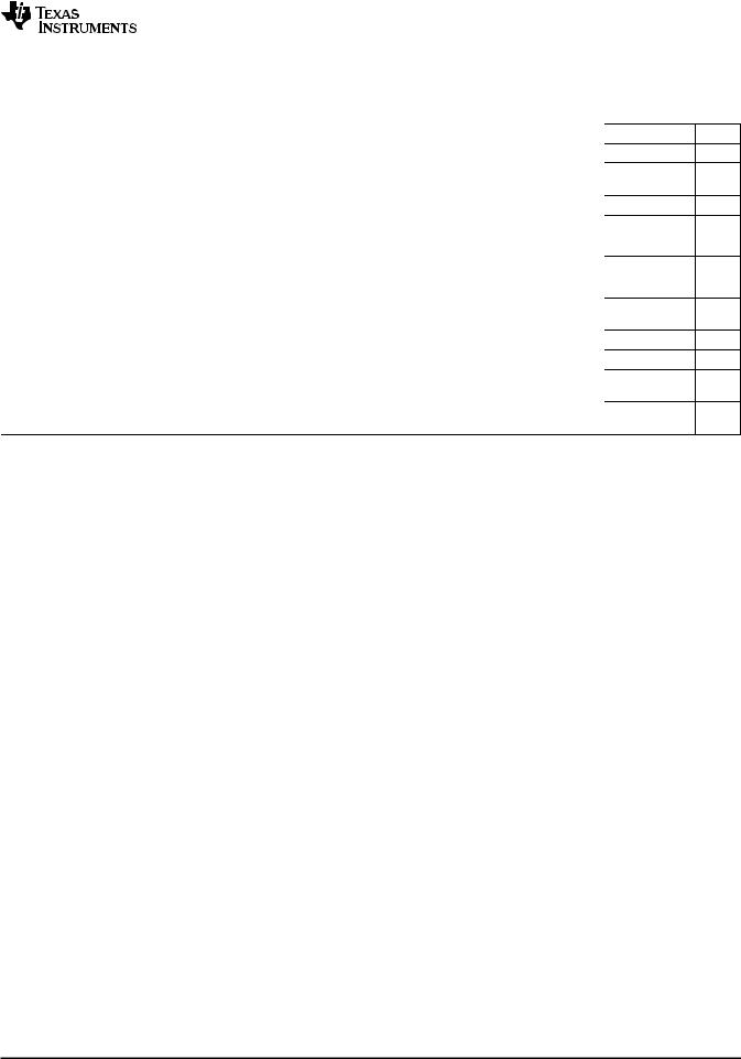
Calibrated DCO Frequencies - Tolerance
over recommended ranges of supply voltage and operating free-air temperature (unless otherwise noted)
PARAMETER |
TEST CONDITIONS |
TA |
VCC |
MIN |
TYP |
MAX |
UNIT |
|
1-MHz tolerance over temperature(1) |
BCSCTL1= CALBC1_1MHz, |
0°C to 85°C |
|
|
±0.5 |
|
|
|
DCOCTL = CALDCO_1MHz, |
3 V |
-3 |
+3 |
% |
||||
|
calibrated at 30°C and 3 V |
-40°C to 105°C |
|
|
|
|
|
|
|
|
|
|
|
|
|
||
|
BCSCTL1= CALBC1_1MHz, |
30°C |
|
|
±2 |
|
|
|
1-MHz tolerance over VCC |
DCOCTL = CALDCO_1MHz, |
1.8 V to 3.6 V |
-3 |
+3 |
% |
|||
|
calibrated at 30°C and 3 V |
|
|
|
|
|
|
|
|
BCSCTL1= CALBC1_1MHz, |
-40°C to 85°C |
|
|
±3 |
|
|
|
1-MHz tolerance overall |
DCOCTL = CALDCO_1MHz, |
1.8 V to 3.6 V |
-6 |
+6 |
% |
|||
-40°C to 105°C |
||||||||
|
calibrated at 30°C and 3 V |
|
|
|
|
|
||
|
|
|
|
|
|
|
(1)This is the frequency change from the measured frequency at 30°C over temperature.
Wake-Up From Lower-Power Modes (LPM3/4) Electrical Characteristics
over recommended ranges of supply voltage and operating free-air temperature (unless otherwise noted)
|
PARAMETER |
TEST CONDITIONS |
VCC |
MIN |
TYP |
MAX |
UNIT |
|
tDCO,LPM3/4 |
DCO clock wake-up time from |
BCSCTL1= CALBC1_1MHz, |
3 V |
|
1.5 |
|
|
µs |
LPM3/4(1) |
DCOCTL = CALDCO_1MHz |
|
|
|
||||
t |
CPU wake-up time from LPM3/4(2) |
|
|
|
1/fMCLK + |
|
|
|
CPU,LPM3/4 |
|
|
|
|
tClock,LPM3/4 |
|
|
|
|
|
|
|
|
|
|
||
(1)The DCO clock wake-up time is measured from the edge of an external wake-up signal (e.g., port interrupt) to the first clock edge observable externally on a clock pin (MCLK or SMCLK).
(2)Parameter applicable only if DCOCLK is used for MCLK.
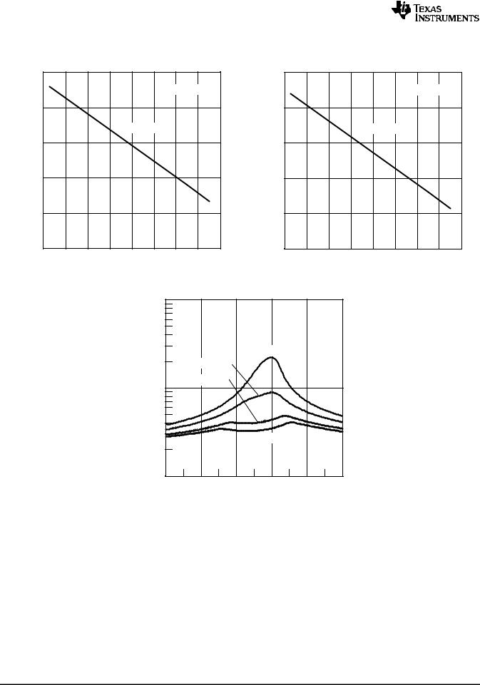
Typical Characteristics - DCO Clock Wake-Up Time From LPM3/4
|
10.00 |
|
|
Time − µs |
|
|
|
Wake |
|
RSELx = 0...11 |
|
1.00 |
|
RSELx = 12...15 |
|
DCO |
|
||
|
|
|
|
|
0.10 |
|
|
|
0.10 |
1.00 |
10.00 |
DCO Frequency − MHz
Figure 13. DCO Wake-Up Time From LPM3 vs DCO Frequency
Copyright © 2010–2011, Texas Instruments Incorporated |
Submit Documentation Feedback |
23 |

MSP430G2x11
MSP430G2x01
SLAS695G –FEBRUARY 2010–REVISED DECEMBER 2011 www.ti.com
Crystal Oscillator, XT1, Low-Frequency Mode(1)
over recommended ranges of supply voltage and operating free-air temperature (unless otherwise noted)
|
PARAMETER |
TEST CONDITIONS |
VCC |
MIN |
TYP |
MAX |
UNIT |
fLFXT1,LF |
LFXT1 oscillator crystal |
XTS = 0, LFXT1Sx = 0 or 1 |
1.8 V to 3.6 V |
|
32768 |
|
Hz |
frequency, LF mode 0, 1 |
|
|
|||||
|
LFXT1 oscillator logic level |
|
|
|
|
|
|
fLFXT1,LF,logic |
square wave input frequency, |
XTS = 0, XCAPx = 0, LFXT1Sx = 3 |
1.8 V to 3.6 V |
10000 |
32768 |
50000 |
Hz |
|
LF mode |
|
|
|
|
|
|
|
|
XTS = 0, LFXT1Sx = 0, |
|
|
500 |
|
|
|
Oscillation allowance for |
fLFXT1,LF = 32768 Hz, CL,eff = 6 pF |
|
|
|
|
|
OALF |
|
|
|
|
kΩ |
||
LF crystals |
XTS = 0, LFXT1Sx = 0, |
|
|
200 |
|
||
|
|
|
|
|
|||
|
|
fLFXT1,LF = 32768 Hz, CL,eff = 12 pF |
|
|
|
|
|
|
|
|
|
|
|
|
|
|
|
XTS = 0, XCAPx = 0 |
|
|
1 |
|
|
|
|
|
|
|
|
|
|
CL,eff |
Integrated effective load |
XTS = 0, XCAPx = 1 |
|
|
5.5 |
|
pF |
capacitance, LF mode(2) |
XTS = 0, XCAPx = 2 |
|
|
8.5 |
|
||
|
|
XTS = 0, XCAPx = 3 |
|
|
11 |
|
|
|
|
|
|
|
|
|
|
|
Duty cycle, LF mode |
XTS = 0, Measured at P2.0/ACLK, |
2.2 V |
30 |
50 |
70 |
% |
|
fLFXT1,LF = 32768 Hz |
||||||
|
|
|
|
|
|
|
|
f |
Oscillator fault frequency, |
XTS = 0, XCAPx = 0, LFXT1Sx = 3(4) |
2.2 V |
10 |
|
10000 |
Hz |
Fault,LF |
LF mode(3) |
|
|
|
|
|
|
(1)To improve EMI on the XT1 oscillator, the following guidelines should be observed.
(a)Keep the trace between the device and the crystal as short as possible.
(b)Design a good ground plane around the oscillator pins.
(c)Prevent crosstalk from other clock or data lines into oscillator pins XIN and XOUT.
(d)Avoid running PCB traces underneath or adjacent to the XIN and XOUT pins.
(e)Use assembly materials and praxis to avoid any parasitic load on the oscillator XIN and XOUT pins.
(f)If conformal coating is used, ensure that it does not induce capacitive/resistive leakage between the oscillator pins.
(g)Do not route the XOUT line to the JTAG header to support the serial programming adapter as shown in other documentation. This signal is no longer required for the serial programming adapter.
(2)Includes parasitic bond and package capacitance (approximately 2 pF per pin).
Since the PCB adds additional capacitance, it is recommended to verify the correct load by measuring the ACLK frequency. For a correct setup, the effective load capacitance should always match the specification of the used crystal.
(3)Frequencies below the MIN specification set the fault flag. Frequencies above the MAX specification do not set the fault flag. Frequencies in between might set the flag.
(4)Measured with logic-level input frequency but also applies to operation with crystals.
Internal Very-Low-Power Low-Frequency Oscillator (VLO)
over recommended ranges of supply voltage and operating free-air temperature (unless otherwise noted)
|
PARAMETER |
TA |
VCC |
MIN |
TYP |
MAX |
UNIT |
fVLO |
VLO frequency |
-40°C to 85°C |
3 V |
4 |
12 |
20 |
kHz |
105°C |
|
|
22 |
||||
|
|
|
|
|
|
||
dfVLO/dT |
VLO frequency temperature drift |
I: -40°C to 85°C |
3 V |
|
0.5 |
|
%/°C |
T: -40°C to 105°C |
|
|
|||||
|
|
|
|
|
|
|
|
dfVLO/dVCC |
VLO frequency supply voltage drift |
25°C |
1.8 V to 3.6 V |
|
4 |
|
%/V |
Timer_A
over recommended ranges of supply voltage and operating free-air temperature (unless otherwise noted)
|
PARAMETER |
TEST CONDITIONS |
VCC |
MIN |
TYP |
MAX |
UNIT |
|
|
|
Internal: SMCLK, ACLK |
|
|
|
|
|
|
fTA |
Timer_A input clock frequency |
External: TACLK, INCLK |
|
|
fSYSTEM |
|
MHz |
|
|
|
Duty cycle = 50% ± 10% |
|
|
|
|
|
|
tTA,cap |
Timer_A capture timing |
TA0, TA1 |
3 V |
20 |
|
|
|
ns |
24 |
Submit Documentation Feedback |
Copyright © 2010–2011, Texas Instruments Incorporated |
MSP430G2x11
MSP430G2x01
www.ti.com |
SLAS695G –FEBRUARY 2010 –REVISED DECEMBER 2011 |
Comparator_A+ (MSP430G2x11 only)
over recommended ranges of supply voltage and operating free-air temperature (unless otherwise noted)
|
|
PARAMETER |
TEST CONDITIONS |
VCC |
MIN |
||
I(DD) |
|
|
|
|
CAON = 1, CARSEL = 0, CAREF = 0 |
3 V |
|
I(Refladder/RefDiode) |
CAON = 1, CARSEL = 0, CAREF = 1/2/3, |
3 V |
|
||||
No load at CA0 and CA1 |
|
||||||
V(IC) |
Common-mode input voltage |
CAON = 1 |
3 V |
0 |
|||
V(Ref025) |
|
Voltage @ 0.25 VCC node |
|
PCA0 = 1, CARSEL = 1, CAREF = 1, |
3 V |
|
|
|
VCC |
No load at CA0 and CA1 |
|
||||
|
|
|
|
||||
V(Ref050) |
|
Voltage @ 0.5 VCC node |
|
PCA0 = 1, CARSEL = 1, CAREF = 2, |
3 V |
|
|
|
VCC |
No load at CA0 and CA1 |
|
||||
|
|
|
|
||||
V(RefVT) |
See Figure 14 and Figure 15 |
PCA0 = 1, CARSEL = 1, CAREF = 3, |
3 V |
|
|||
No load at CA0 and CA1, TA = 85°C |
|
||||||
|
|
|
|
|
|
|
|
V |
Offset voltage(1) |
|
3 V |
|
|||
(offset) |
|
|
|
|
|
|
|
Vhys |
Input hysteresis |
CAON = 1 |
3 V |
|
|||
|
|
|
|
|
TA = 25°C, Overdrive 10 mV, |
|
|
t(response) |
Response time |
Without filter: CAF = 0 |
3 V |
|
|||
(low-high and high-low) |
TA = 25°C, Overdrive 10 mV, |
|
|||||
|
|
|
|
|
With filter: CAF = 1 |
|
|
|
|
|
|
|
|
|
|
TYP MAX UNIT
45 µA
45 µA
VCC-1 V
0.24
0.48
490 mV
±10 mV
0.7mV
120 ns
1.5µs
(1)The input offset voltage can be cancelled by using the CAEX bit to invert the Comparator_A+ inputs on successive measurements. The two successive measurements are then summed together.
Copyright © 2010–2011, Texas Instruments Incorporated |
Submit Documentation Feedback |
25 |
MSP430G2x11
MSP430G2x01
SLAS695G –FEBRUARY 2010–REVISED DECEMBER 2011 |
www.ti.com |
Typical Characteristics - Comparator_A+
|
650 |
|
|
|
|
|
|
|
|
|
|
|
|
|
|
|
VCC = 3 V |
|
|
mV |
600 |
|
|
|
|
|
|
|
|
– |
|
|
|
|
|
|
|
|
|
Voltage |
|
|
|
|
Typical |
|
|
|
|
550 |
|
|
|
|
|
|
|
|
|
–Reference |
500 |
|
|
|
|
|
|
|
|
|
|
|
|
|
|
|
|
|
|
(RefVT) |
450 |
|
|
|
|
|
|
|
|
V |
|
|
|
|
|
|
|
|
|
|
400 |
|
|
|
|
|
|
|
|
|
-45 |
-25 |
-5 |
15 |
35 |
55 |
75 |
95 |
115 |
|
|
|
TA – Free-Air Temperature – °C |
|
|
||||
|
650 |
|
|
|
|
|
|
|
|
|
|
|
|
|
|
|
VCC = 2.2 V |
|
|
mV |
600 |
|
|
|
|
|
|
|
|
– |
|
|
|
|
|
|
|
|
|
Voltage |
|
|
|
|
Typical |
|
|
|
|
550 |
|
|
|
|
|
|
|
|
|
–Reference |
500 |
|
|
|
|
|
|
|
|
|
|
|
|
|
|
|
|
|
|
(RefVT) |
450 |
|
|
|
|
|
|
|
|
V |
|
|
|
|
|
|
|
|
|
|
400 |
|
|
|
|
|
|
|
|
|
-45 |
-25 |
-5 |
15 |
35 |
55 |
75 |
95 |
115 |
|
|
|
TA – Free-Air Temperature – °C |
|
|
||||
Figure 14. V(RefVT) vs Temperature, VCC = 3 V |
Figure 15. V(RefVT) vs Temperature, VCC = 2.2 V |
100
kΩ |
|
VCC = 1.8 V |
|
– |
VCC |
= 2.2 V |
|
Short Resistance |
|||
VCC = 3 V |
|||
10 |
|
||
|
|
||
|
|
VCC = 3.6 V |
|
1
0 |
0.2 |
0.4 |
0.6 |
0.8 |
1 |
|
VIN/VCC – Normalized Input |
Voltage – V/V |
|
||
Figure 16. Short Resistance vs VIN/VCC
26 |
Submit Documentation Feedback |
Copyright © 2010–2011, Texas Instruments Incorporated |