


|
|
MSP430G2x11 |
|
|
MSP430G2x01 |
www.ti.com |
SLAS695G –FEBRUARY 2010 –REVISED DECEMBER 2011 |
|
Absolute Maximum Ratings(1) |
|
|
Voltage applied at VCC to VSS |
|
-0.3 V to 4.1 V |
Voltage applied to any pin(2) |
|
-0.3 V to V + 0.3 V |
|
|
CC |
Diode current at any device pin |
|
±2 mA |
(3) |
Unprogrammed device |
-55°C to 150°C |
Storage temperature range, Tstg |
Programmed device |
-55°C to 150°C |
|
||
(1)Stresses beyond those listed under "absolute maximum ratings" may cause permanent damage to the device. These are stress ratings only, and functional operation of the device at these or any other conditions beyond those indicated under "recommended operating conditions" is not implied. Exposure to absolute-maximum-rated conditions for extended periods may affect device reliability.
(2)All voltages referenced to VSS. The JTAG fuse-blow voltage, VFB, is allowed to exceed the absolute maximum rating. The voltage is applied to the TEST pin when blowing the JTAG fuse.
(3)Higher temperature may be applied during board soldering according to the current JEDEC J-STD-020 specification with peak reflow temperatures not higher than classified on the device label on the shipping boxes or reels.
Recommended Operating Conditions
|
|
|
MIN |
NOM MAX |
UNIT |
|
|
|
|
|
|
|
|
VCC |
Supply voltage |
During program execution |
1.8 |
3.6 |
V |
|
|
|
|
||||
During flash program/erase |
2.2 |
3.6 |
||||
|
|
|
||||
|
|
|
|
|
|
|
VSS |
Supply voltage |
|
|
0 |
V |
|
TA |
Operating free-air temperature |
I version |
-40 |
85 |
°C |
|
|
|
|
||||
T version |
-40 |
105 |
||||
|
|
|
||||
|
|
|
|
|
|
|
|
|
VCC = 1.8 V, |
dc |
6 |
|
|
|
|
Duty cycle = 50% ± 10% |
|
|
|
|
f |
Processor frequency (maximum MCLK frequency)(1)(2) |
VCC = 2.7 V, |
dc |
12 |
MHz |
|
SYSTEM |
|
Duty cycle = 50% ± 10% |
|
|
|
|
|
|
|
|
|
||
|
|
VCC ≥ 3.3 V, |
dc |
16 |
|
|
|
|
Duty cycle = 50% ± 10% |
|
|||
|
|
|
|
|
(1)The MSP430 CPU is clocked directly with MCLK. Both the high and low phase of MCLK must not exceed the pulse width of the specified maximum frequency.
(2)Modules might have a different maximum input clock specification. See the specification of the respective module in this data sheet.
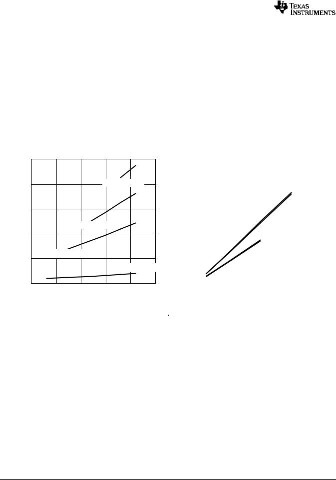
System Frequency - MHz
Legend :
16 MHz
Supply voltage range,
during flash memory
programming
12 MHz
Supply voltage range, during program execution
6 MHz
1.8 V |
2.2 V |
2.7 V |
3.3 V 3.6 V |
Supply Voltage - V
Note: Minimum processor frequency is defined by system clock. Flash program or erase operations require a minimum VCC of 2.2 V.
Figure 1. Safe Operating Area
Copyright © 2010–2011, Texas Instruments Incorporated |
Submit Documentation Feedback |
15 |
MSP430G2x11
MSP430G2x01
SLAS695G –FEBRUARY 2010–REVISED DECEMBER 2011 |
www.ti.com |
Electrical Characteristics
Active Mode Supply Current Into VCC Excluding External Current
over recommended ranges of supply voltage and operating free-air temperature (unless otherwise noted)(1)(2)
|
PARAMETER |
TEST CONDITIONS |
TA |
VCC |
MIN TYP |
MAX |
UNIT |
|
|
fDCO = fMCLK = fSMCLK = 1 MHz, |
|
2.2 V |
220 |
|
|
|
|
fACLK = 32768 Hz, |
|
|
|
|
|
|
Active mode (AM) |
Program executes in flash, |
|
|
|
|
µA |
IAM,1MHz |
BCSCTL1 = CALBC1_1MHZ, |
|
|
|
|
||
current (1 MHz) |
|
3 V |
300 |
370 |
|||
|
DCOCTL = CALDCO_1MHZ, |
|
|
||||
|
|
CPUOFF = 0, SCG0 = 0, SCG1 = 0, |
|
|
|
|
|
|
|
OSCOFF = 0 |
|
|
|
|
|
|
|
|
|
|
|
|
|
(1)All inputs are tied to 0 V or to VCC. Outputs do not source or sink any current.
(2)The currents are characterized with a Micro Crystal CC4V-T1A SMD crystal with a load capacitance of 9 pF. The internal and external load capacitance is chosen to closely match the required 9 pF.
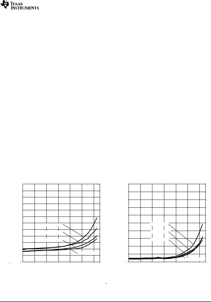
Typical Characteristics - Active Mode Supply Current (Into VCC)
|
5.0 |
|
|
|
4.0 |
fDCO = 16 MHz |
|
− mA |
|
|
− mA |
Current |
3.0 |
|
Current |
|
|
|
|
Mode |
2.0 |
fDCO = 12 MHz |
Mode |
|
|
|
|
Active |
|
fDCO = 8 MHz |
Active |
|
1.0 |
|
|
|
|
|
|
|
|
fDCO = 1 MHz |
|
0.0 |
|
|
|
|
|
1.5 |
2.0 |
2.5 |
3.0 |
3.5 |
4.0 |
VCC − Supply Voltage − V
Figure 2. Active Mode Current vs VCC, TA = 25°C
4.0 |
|
|
|
|
|
|
|
|
|
|
|
|
|
|
|
|
|
|
|
|
|
|
|
|
|
|
|
|
|
|
||
3.0 |
|
|
|
|
|
|
|
TA = 85 °C |
|
|
|
|
|
|
|
|
|
|
|
|
|
|
|
|
|
|
|
|
|
|
|
|
|
|
|
|
|
|
|
|
|
|
|
|
|
|
|
|
|
|
|
TA = 25 °C |
|
|
|
|
|
|
|
|
|
|
|
|
|
2.0 |
|
VCC = 3 V |
|
|
|
|
|
|
|
|
|
|
|
|
|
|
|
|
|
|
|
|
|
|
|
|
|
|
|
|
|
|
|
|
|
|
|
|
|
|
|
|
|
|
|
|
|
|
TA = 85 °C |
|
|
|
|
|
|
|
|
|
|
|
|
|
|
|
|
|
|
|
|
|
TA = 25 °C |
|
|
|
||
1.0 |
|
|
|
|
|
|
|
|
|
|
|
|
|
|
|
|
|
|
|
|
|
|
|
|
|
|
|
|
|
|
|
|
|
|
VCC = 2.2 V |
|
|
|
|
||||
0.0 |
|
|
|
|
|
|
|
|
|
|
|
|
|
|
|
|
|
|
|
|
|
0.0 |
4.0 |
8.0 |
12.0 |
16.0 |
|
fDCO − DCO Frequency − MHz |
|
||
Figure 3. Active Mode Current vs DCO Frequency
16 |
Submit Documentation Feedback |
Copyright © 2010–2011, Texas Instruments Incorporated |
MSP430G2x11
MSP430G2x01
www.ti.com |
SLAS695G –FEBRUARY 2010 –REVISED DECEMBER 2011 |
Low-Power Mode Supply Currents (Into VCC) Excluding External Current
over recommended ranges of supply voltage and operating free-air temperature (unless otherwise noted)(1) (2)
PARAMETER |
|
TEST CONDITIONS |
TA |
VCC |
MIN TYP |
MAX |
UNIT |
||
|
|
|
fMCLK = 0 MHz, |
|
|
|
|
|
|
|
|
|
fSMCLK = fDCO = 1 MHz, |
|
|
|
|
|
|
|
Low-power mode 0 |
fACLK = 32768 Hz, |
25°C |
|
|
|
µA |
||
ILPM0,1MHz |
(LPM0) current(3) |
BCSCTL1 = CALBC1_1MHZ, |
2.2 V |
65 |
|
||||
|
|
|
DCOCTL = CALDCO_1MHZ, |
|
|
|
|
|
|
|
|
|
CPUOFF = 1, SCG0 = 0, SCG1 = 0, |
|
|
|
|
|
|
|
|
|
OSCOFF = 0 |
|
|
|
|
|
|
|
|
|
|
|
|
|
|
|
|
|
|
|
fMCLK = fSMCLK = 0 MHz, |
25°C |
|
22 |
|
|
|
|
|
|
fDCO = 1 MHz, |
|
|
|
|
|
|
ILPM2 |
Low-power mode 2 |
fACLK = 32768 Hz, |
|
2.2 V |
|
|
µA |
||
(LPM2) current |
(4) |
BCSCTL1 = CALBC1_1MHZ, |
105°C |
|
31 |
||||
|
|
DCOCTL = CALDCO_1MHZ, |
|
|
|
||||
|
|
|
CPUOFF = 1, SCG0 = 0, SCG1 = 1, |
|
|
|
|
|
|
|
|
|
OSCOFF = 0 |
|
|
|
|
|
|
|
|
|
|
|
|
|
|
|
|
|
|
|
fDCO = fMCLK = fSMCLK = 0 MHz, |
25°C |
|
0.7 |
1.5 |
|
|
ILPM3,LFXT1 |
Low-power mode 3 |
fACLK = 32768 Hz, |
|
2.2 V |
|
|
µA |
||
(LPM3) current(4) |
CPUOFF = 1, SCG0 = 1, SCG1 = 1, |
105°C |
3 |
6 |
|||||
|
|
|
OSCOFF = 0 |
|
|
|
|
|
|
|
|
|
fDCO = fMCLK = fSMCLK = 0 MHz, |
25°C |
|
0.5 |
0.7 |
|
|
ILPM3,VLO |
Low-power mode 3 |
fACLK from internal LF oscillator (VLO), |
|
2.2 V |
|
|
µA |
||
|
|
|
|||||||
current, (LPM3)(4) |
CPUOFF = 1, SCG0 = 1, SCG1 = 1, |
105°C |
2 |
5 |
|||||
|
|
|
OSCOFF = 0 |
|
|
|
|
|
|
|
|
|
fDCO = fMCLK = fSMCLK = 0 MHz, |
25°C |
|
0.1 |
0.5 |
|
|
ILPM4 |
Low-power mode 4 |
fACLK = 0 Hz, |
85°C |
2.2 V |
0.8 |
1.5 |
µA |
||
(LPM4) current(5) |
CPUOFF = 1, SCG0 = 1, SCG1 = 1, |
||||||||
|
105°C |
|
2 |
4 |
|
||||
|
|
|
OSCOFF = 1 |
|
|
||||
(1)All inputs are tied to 0 V or to VCC. Outputs do not source or sink any current.
(2)The currents are characterized with a Micro Crystal CC4V-T1A SMD crystal with a load capacitance of 9 pF.
(3)Current for brownout and WDT clocked by SMCLK included.
(4)Current for brownout and WDT clocked by ACLK included.
(5)Current for brownout included.
Typical Characteristics Low-Power Mode Supply Currents
over recommended ranges of supply voltage and operating free-air temperature (unless otherwise noted)
|
3.00 |
|
|
|
|
|
|
|
2.75 |
|
|
|
|
|
|
µA |
2.50 |
|
|
|
|
|
|
– |
|
|
|
|
|
|
|
Current |
2.25 |
|
|
|
|
|
|
2.00 |
|
|
|
|
|
|
|
|
|
|
|
|
|
|
|
Mode |
1.75 |
|
|
|
|
|
|
1.50 |
|
|
|
|
|
|
|
Power |
|
Vcc = 3.6 V |
|
|
|
||
|
|
|
|
|
|||
1.25 |
|
|
|
|
|
|
|
|
|
Vcc = 3 V |
|
|
|
||
- |
1.00 |
|
|
|
|
|
|
Low |
|
|
|
|
|
|
|
0.75 |
|
Vcc = 2.2 V |
|
|
|
||
– |
|
|
|
|
|
|
|
LPM3 |
0.50 |
|
|
|
|
|
|
|
|
|
|
|
|
|
|
I |
|
|
|
|
|
Vcc = 1.8 V |
|
|
0.25 |
|
|
|
|
||
|
|
|
|
|
|
|
|
|
0.00 |
|
|
|
|
|
|
|
-40 |
-20 |
0 |
20 |
40 |
60 |
80 |
|
|
|
TA – Temperature – °C |
|
|
||
Figure 4. LPM3 Current vs Temperature
|
2.50 |
|
|
|
|
|
|
– µA |
2.25 |
|
|
|
|
|
|
2.00 |
|
|
|
|
|
|
|
Current |
|
|
|
|
|
|
|
1.75 |
|
|
|
|
|
|
|
|
|
|
|
|
|
|
|
Mode |
1.50 |
|
|
|
|
|
|
1.25 |
|
|
|
|
|
|
|
Power |
|
Vcc = 3.6 V |
|
|
|
||
|
|
|
|
|
|||
1.00 |
|
Vcc = 3 V |
|
|
|
||
- |
|
|
|
|
|
|
|
Low |
0.75 |
|
Vcc = 2.2 V |
|
|
|
|
|
|
|
|
|
|||
– |
|
|
|
|
|
||
|
|
|
|
|
|
|
|
LPM4 |
0.50 |
|
|
|
|
|
|
|
|
|
|
|
|
|
|
I |
|
|
|
|
|
|
|
|
0.25 |
|
|
|
|
|
|
|
0.00 |
|
|
|
|
Vcc = 1.8 V |
|
|
|
|
|
|
|
|
|
|
-40 |
-20 |
0 |
20 |
40 |
60 |
80 |
|
|
|
TA – Temperature – °C |
|
|
||
Figure 5. LPM4 Current vs Temperature
Copyright © 2010–2011, Texas Instruments Incorporated |
Submit Documentation Feedback |
17 |

MSP430G2x11
MSP430G2x01
SLAS695G –FEBRUARY 2010–REVISED DECEMBER 2011 www.ti.com
Schmitt-Trigger Inputs - Ports Px
over recommended ranges of supply voltage and operating free-air temperature (unless otherwise noted)
|
PARAMETER |
TEST CONDITIONS |
VCC |
MIN |
TYP |
MAX |
UNIT |
|
VIT+ |
Positive-going input threshold voltage |
|
|
0.45 VCC |
|
0.75 VCC |
V |
|
|
3 V |
1.35 |
|
2.25 |
||||
|
|
|
|
|
||||
|
|
|
|
|
|
|
|
|
VIT- |
Negative-going input threshold voltage |
|
|
0.25 VCC |
|
0.55 VCC |
V |
|
|
3 V |
0.75 |
|
1.65 |
||||
|
|
|
|
|
||||
|
|
|
|
|
|
|
|
|
Vhys |
Input voltage hysteresis (VIT+ - VIT-) |
|
3 V |
0.3 |
|
1 |
V |
|
RPull |
Pullup/pulldown resistor |
For pullup: VIN = VSS |
3 V |
20 |
35 |
50 |
kΩ |
|
For pulldown: VIN = VCC |
||||||||
|
|
|
|
|
|
|
||
CI |
Input capacitance |
VIN = VSS or VCC |
|
|
5 |
|
pF |
Leakage Current - Ports Px
over recommended ranges of supply voltage and operating free-air temperature (unless otherwise noted)
|
PARAMETER |
|
TEST CONDITIONS |
VCC |
MIN MAX |
UNIT |
Ilkg(Px.x) |
High-impedance leakage current |
(1) |
(2) |
3 V |
±50 |
nA |
|
|
(1)The leakage current is measured with VSS or VCC applied to the corresponding pin(s), unless otherwise noted.
(2)The leakage of the digital port pins is measured individually. The port pin is selected for input and the pullup/pulldown resistor is disabled.
Outputs - Ports Px
over recommended ranges of supply voltage and operating free-air temperature (unless otherwise noted)
|
|
PARAMETER |
|
|
TEST CONDITIONS |
VCC |
MIN |
TYP |
MAX |
UNIT |
V |
OH |
High-level output voltage |
I |
(OHmax) |
= -6 mA(1) |
3 V |
V |
- 0.3 |
|
V |
|
|
|
|
|
CC |
|
|
|
||
V |
OL |
Low-level output voltage |
I |
(OLmax) |
= 6 mA(1) |
3 V |
V |
+ 0.3 |
|
V |
|
|
|
|
|
SS |
|
|
|
(1)The maximum total current, I(OHmax) and I(OLmax), for all outputs combined should not exceed ±48 mA to hold the maximum voltage drop specified.
Output Frequency - Ports Px
over recommended ranges of supply voltage and operating free-air temperature (unless otherwise noted)
|
PARAMETER |
TEST CONDITIONS |
VCC |
MIN TYP |
MAX |
UNIT |
fPx.y |
Port output frequency |
Px.y, CL = 20 pF, RL = 1 kΩ(1) (2) |
3 V |
12 |
|
MHz |
|
(with load) |
|
|
|
|
|
f |
Clock output frequency |
Px.y, C = 20 pF(2) |
3 V |
16 |
|
MHz |
Port_CLK |
|
L |
|
|
|
|
(1)A resistive divider with 2 × 0.5 kΩ between VCC and VSS is used as load. The output is connected to the center tap of the divider.
(2)The output voltage reaches at least 10% and 90% VCC at the specified toggle frequency.
18 |
Submit Documentation Feedback |
Copyright © 2010–2011, Texas Instruments Incorporated |