

MSP430G2x11
MSP430G2x01
www.ti.com |
SLAS695G –FEBRUARY 2010 –REVISED DECEMBER 2011 |
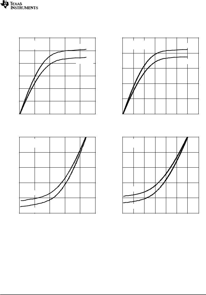
Typical Characteristics - Outputs
over recommended ranges of supply voltage and operating free-air temperature (unless otherwise noted)
|
30 |
|
|
|
|
|
− mA |
|
VCC = 2.2 V |
|
|
TA = 25°C |
|
|
P1.7 |
|
|
|||
25 |
|
|
|
|
|
|
Current |
20 |
|
|
|
TA = 85°C |
|
|
|
|
|
|
||
Output |
|
|
|
|
|
|
|
|
|
|
|
|
|
Low-Level |
15 |
|
|
|
|
|
10 |
|
|
|
|
|
|
Typical |
5 |
|
|
|
|
|
− |
|
|
|
|
|
|
OL |
|
|
|
|
|
|
I |
|
|
|
|
|
|
|
0 |
|
|
|
|
|
|
0 |
0.5 |
1 |
1.5 |
2 |
2.5 |
|
|
VOL − Low-Level Output Voltage − V |
|
|||
Figure 6.
|
0 |
|
|
|
|
|
− mA |
|
VCC = 2.2 V |
|
|
|
|
|
P1.7 |
|
|
|
|
|
−5 |
|
|
|
|
|
|
Current |
|
|
|
|
|
|
|
|
|
|
|
|
|
-Level Output |
−10 |
|
|
|
|
|
−15 |
|
|
|
|
|
|
High |
|
|
|
|
|
|
|
|
|
|
|
|
|
− Typical |
|
TA = 85°C |
|
|
|
|
−20 |
|
|
|
|
|
|
|
|
|
|
|
|
|
OH |
|
|
|
|
|
|
I |
|
|
|
|
|
|
|
−25 |
TA = 25°C |
|
|
|
|
|
|
|
|
|
|
|
|
0 |
0.5 |
1 |
1.5 |
2 |
2.5 |
|
|
VOH − High-Level Output Voltage − V |
|
|||
Figure 8.
|
50 |
|
|
|
|
|
|
|
− mA |
|
VCC = 3 V |
|
|
|
|
TA = 25°C |
|
|
P1.7 |
|
|
|
|
|
||
40 |
|
|
|
|
|
|
|
|
Current |
|
|
|
|
|
|
|
|
|
|
|
|
|
|
TA = 85°C |
|
|
|
|
|
|
|
|
|
|
|
-Level Output |
30 |
|
|
|
|
|
|
|
20 |
|
|
|
|
|
|
|
|
Low |
|
|
|
|
|
|
|
|
− Typical |
10 |
|
|
|
|
|
|
|
|
|
|
|
|
|
|
|
|
OL |
|
|
|
|
|
|
|
|
I |
|
|
|
|
|
|
|
|
|
0 |
|
|
|
|
|
|
|
|
0 |
0.5 |
1 |
1.5 |
2 |
2.5 |
3 |
3.5 |
|
|
VOL − Low-Level Output Voltage − V |
|
|||||
Figure 7.
|
0 |
|
|
|
|
|
|
|
− mA |
|
VCC = 3 V |
|
|
|
|
|
|
|
P1.7 |
|
|
|
|
|
|
|
−10 |
|
|
|
|
|
|
|
|
Current |
|
|
|
|
|
|
|
|
|
|
|
|
|
|
|
|
|
-Level Output |
−20 |
|
|
|
|
|
|
|
−30 |
|
|
|
|
|
|
|
|
High |
|
|
|
|
|
|
|
|
|
TA = 85°C |
|
|
|
|
|
|
|
− Typical |
|
|
|
|
|
|
|
|
−40 |
|
|
|
|
|
|
|
|
|
|
|
|
|
|
|
|
|
OH |
|
T = 25°C |
|
|
|
|
|
|
I |
|
A |
|
|
|
|
|
|
|
−50 |
|
|
|
|
|
|
|
|
0 |
0.5 |
1 |
1.5 |
2 |
2.5 |
3 |
3.5 |
|
|
VOH − High-Level Output Voltage − V |
|
|
||||
Figure 9.
Copyright © 2010–2011, Texas Instruments Incorporated |
Submit Documentation Feedback |
19 |

MSP430G2x11
MSP430G2x01
SLAS695G –FEBRUARY 2010–REVISED DECEMBER 2011 www.ti.com
POR/Brownout Reset (BOR)(1)
over recommended ranges of supply voltage and operating free-air temperature (unless otherwise noted)
|
PARAMETER |
TEST CONDITIONS |
VCC |
MIN |
TYP |
MAX |
UNIT |
||
VCC(start) |
See Figure 10 |
dVCC/dt ≤ 3 V/s |
|
|
0.7 × |
|
V |
||
|
|
V(B_IT-) |
|
||||||
|
|
|
|
|
|
|
|
|
|
V(B_IT-) |
See Figure 10 through Figure 12 |
dVCC/dt ≤ 3 V/s |
|
|
1.35 |
|
V |
||
Vhys(B_IT-) |
See Figure 10 |
dVCC/dt ≤ 3 V/s |
|
|
130 |
|
mV |
||
td(BOR) |
See Figure 10 |
|
|
|
|
2000 |
µs |
||
|
Pulse length needed at |
|
|
|
|
|
|
|
|
t(reset) |
RST/NMI pin to |
|
2.2 V/3 V |
2 |
|
|
µs |
||
accepted reset internally |
|
|
|
||||||
|
|
|
|
|
|
|
|||
|
|
|
|
|
|
|
|
|
|
(1)The current consumption of the brownout module is already included in the ICC current consumption data. The voltage level V(B_IT-) + Vhys(B_IT-)is ≤ 1.8 V.
VCC |
Vhys(B_IT−) |
V(B_IT−) |
VCC(star t) |
1 |
0 |
t d(BOR) |
Figure 10. POR/Brownout Reset (BOR) vs Supply Voltage
20 |
Submit Documentation Feedback |
Copyright © 2010–2011, Texas Instruments Incorporated |
MSP430G2x11
MSP430G2x01
www.ti.com |
SLAS695G –FEBRUARY 2010 –REVISED DECEMBER 2011 |
Typical Characteristics - POR/Brownout Reset (BOR)
|
2 |
|
|
|
|
VCC = 3 V |
|
|
|
Typical Conditions |
|
V |
1.5 |
|
|
− |
|
|
|
CC(drop) |
1 |
|
|
|
|
|
|
V |
0.5 |
|
|
|
|
|
|
|
0 |
|
|
|
0.001 |
1 |
1000 |
|
|
tpw − Pulse Width − µs |
|
VCC |
t |
pw |
|
|
|
3 V |
|
|
VCC(drop) |
|
|
1 ns |
|
1 ns |
|
tpw − Pulse Width − µs |
|
VCC(drop) − V
Figure 11. VCC(drop) Level With a Square Voltage Drop to Generate a POR/Brownout Signal
2 |
|
|
|
|
VCC = 3 V |
|
|
1.5 |
Typical Conditions |
|
|
1 |
|
|
|
0.5 |
|
|
|
0 |
|
|
|
0.001 |
1 |
1000 |
|
|
|
tpw − Pulse Width − µs |
|
VCC |
t pw |
3 V |
|
VCC(drop) |
|
|
tf = tr |
tf |
tr |
tpw − Pulse Width − µs |
|
Figure 12. VCC(drop) Level With a Triangle Voltage Drop to Generate a POR/Brownout Signal
Copyright © 2010–2011, Texas Instruments Incorporated |
Submit Documentation Feedback |
21 |

MSP430G2x11
MSP430G2x01
SLAS695G –FEBRUARY 2010–REVISED DECEMBER 2011 |
www.ti.com |
Main DCO Characteristics
•All ranges selected by RSELx overlap with RSELx + 1: RSELx = 0 overlaps RSELx = 1, ... RSELx = 14 overlaps RSELx = 15.
•DCO control bits DCOx have a step size as defined by parameter SDCO.
•Modulation control bits MODx select how often fDCO(RSEL,DCO+1) is used within the period of 32 DCOCLK
cycles. The frequency fDCO(RSEL,DCO) is used for the remaining cycles. The frequency is an average equal to:
faverage =
32 × fDCO(RSEL,DCO) × fDCO(RSEL,DCO+1)
MOD × fDCO(RSEL,DCO) + (32 – MOD) × fDCO(RSEL,DCO+1)
DCO Frequency
over recommended ranges of supply voltage and operating free-air temperature (unless otherwise noted)
|
PARAMETER |
TEST CONDITIONS |
VCC |
MIN |
TYP MAX |
UNIT |
|
|
|
RSELx < 14 |
|
1.8 |
3.6 |
V |
|
VCC |
Supply voltage |
RSELx = 14 |
|
2.2 |
3.6 |
V |
|
|
|
RSELx = 15 |
|
3 |
3.6 |
V |
|
|
|
|
|
|
|
|
|
fDCO(0,0) |
DCO frequency (0, 0) |
RSELx = 0, DCOx = 0, MODx = 0 |
3 V |
0.06 |
0.14 |
MHz |
|
fDCO(0,3) |
DCO frequency (0, 3) |
RSELx = 0, DCOx = 3, MODx = 0 |
3 V |
|
0.12 |
|
MHz |
fDCO(1,3) |
DCO frequency (1, 3) |
RSELx = 1, DCOx = 3, MODx = 0 |
3 V |
|
0.15 |
|
MHz |
fDCO(2,3) |
DCO frequency (2, 3) |
RSELx = 2, DCOx = 3, MODx = 0 |
3 V |
|
0.21 |
|
MHz |
fDCO(3,3) |
DCO frequency (3, 3) |
RSELx = 3, DCOx = 3, MODx = 0 |
3 V |
|
0.3 |
|
MHz |
fDCO(4,3) |
DCO frequency (4, 3) |
RSELx = 4, DCOx = 3, MODx = 0 |
3 V |
|
0.41 |
|
MHz |
fDCO(5,3) |
DCO frequency (5, 3) |
RSELx = 5, DCOx = 3, MODx = 0 |
3 V |
|
0.58 |
|
MHz |
fDCO(6,3) |
DCO frequency (6, 3) |
RSELx = 6, DCOx = 3, MODx = 0 |
3 V |
|
0.8 |
|
MHz |
fDCO(7,3) |
DCO frequency (7, 3) |
RSELx = 7, DCOx = 3, MODx = 0 |
3 V |
0.8 |
1.5 |
MHz |
|
fDCO(8,3) |
DCO frequency (8, 3) |
RSELx = 8, DCOx = 3, MODx = 0 |
3 V |
|
1.6 |
|
MHz |
fDCO(9,3) |
DCO frequency (9, 3) |
RSELx = 9, DCOx = 3, MODx = 0 |
3 V |
|
2.3 |
|
MHz |
fDCO(10,3) |
DCO frequency (10, 3) |
RSELx = 10, DCOx = 3, MODx = 0 |
3 V |
|
3.4 |
|
MHz |
fDCO(11,3) |
DCO frequency (11, 3) |
RSELx = 11, DCOx = 3, MODx = 0 |
3 V |
|
4.25 |
|
MHz |
fDCO(12,3) |
DCO frequency (12, 3) |
RSELx = 12, DCOx = 3, MODx = 0 |
3 V |
4.3 |
7.3 |
MHz |
|
fDCO(13,3) |
DCO frequency (13, 3) |
RSELx = 13, DCOx = 3, MODx = 0 |
3 V |
|
7.8 |
|
MHz |
fDCO(14,3) |
DCO frequency (14, 3) |
RSELx = 14, DCOx = 3, MODx = 0 |
3 V |
8.6 |
13.9 |
MHz |
|
fDCO(15,3) |
DCO frequency (15, 3) |
RSELx = 15, DCOx = 3, MODx = 0 |
3 V |
|
15.25 |
|
MHz |
fDCO(15,7) |
DCO frequency (15, 7) |
RSELx = 15, DCOx = 7, MODx = 0 |
3 V |
|
21 |
|
MHz |
|
Frequency step between |
|
|
|
|
|
|
SRSEL |
range RSEL and |
SRSEL = fDCO(RSEL+1,DCO)/fDCO(RSEL,DCO) |
3 V |
|
1.35 |
|
ratio |
|
RSEL+1 |
|
|
|
|
|
|
SDCO |
Frequency step between |
SDCO = fDCO(RSEL,DCO+1)/fDCO(RSEL,DCO) |
3 V |
|
1.08 |
|
ratio |
tap DCO and DCO+1 |
|
|
|||||
|
Duty cycle |
Measured at SMCLK output |
3 V |
|
50 |
|
% |
|
|
|
|
|
|
|
|
22 |
Submit Documentation Feedback |
Copyright © 2010–2011, Texas Instruments Incorporated |