

STM32F100x4, STM32F100x6, STM32F100x8, STM32F100xB |
Electrical characteristics |
|
|
5 Electrical characteristics
5.1Parameter conditions
Unless otherwise specified, all voltages are referenced to VSS.
5.1.1Minimum and maximum values
Unless otherwise specified the minimum and maximum values are guaranteed in the worst conditions of ambient temperature, supply voltage and frequencies by tests in production on 100% of the devices with an ambient temperature at TA = 25 °C and TA = TAmax (given by the selected temperature range).
Data based on characterization results, design simulation and/or technology characteristics are indicated in the table footnotes and are not tested in production. Based on characterization, the minimum and maximum values refer to sample tests and represent the mean value plus or minus three times the standard deviation (mean±3 ).
5.1.2Typical values
Unless otherwise specified, typical data are based on TA = 25 °C, VDD = 3.3 V (for the 2 V VDD 3.6 V voltage range). They are given only as design guidelines and are not tested.
Typical ADC accuracy values are determined by characterization of a batch of samples from a standard diffusion lot over the full temperature range, where 95% of the devices have an error less than or equal to the value indicated (mean±2 ).
5.1.3Typical curves
Unless otherwise specified, all typical curves are given only as design guidelines and are not tested.
5.1.4Loading capacitor
The loading conditions used for pin parameter measurement are shown in Figure 8.
5.1.5Pin input voltage
The input voltage measurement on a pin of the device is described in Figure 9.
Doc ID 16455 Rev 3 |
31/86 |
Electrical characteristics |
STM32F100x4, STM32F100x6, STM32F100x8, STM32F100xB |
|
|
|
|
Figure 8. Pin loading conditions |
Figure 9. Pin input voltage |
|
C = 50 pF |
|
|
|
|
|
|
|
|
|
|
|
|
|
STM32F10xxx pin |
|
|
V |
|
|
|
|
|
|
|
|
|
STM32F10xxx pin |
|||
|
|
|
|
|
|
|
|
|
|
|
|
|
|
|
|
|
|
|
|
|
|
|
|
|||||||
|
|
|
|
|
|
|
|
|
|
|
|
|
IN |
|
|
|
|
|||||||||||||
|
|
|
|
|
|
|
|
|
|
|
|
|
|
|
|
|
||||||||||||||
|
|
|
|
|
|
|
|
|
|
|
|
|
|
|
|
|
|
|
|
|
|
|
|
|
|
|
|
|
|
|
|
|
|
|
|
|
|
|
|
|
|
|
|
|
|
ai14123b |
|
|
|
|
|
|
|
|
|
|
|
|
|
ai14124b |
|
|
|
|
|
|
|
|
|
|
|
|
|
|
|
|
|
|
|
|
|
|
|
|
|
|
|
|
|
|||
|
|
|
|
|
|
|
|
|
|
|
|
|
|
|
|
|
|
|
|
|
|
|
|
|
|
|
|
|||
|
|
|
|
|
|
|
|
|
|
|
|
|
|
|
|
|
|
|
|
|
|
|
|
|
|
|
|
|||
|
|
|
|
|
|
|
|
|
|
|
|
|
|
|
|
|
|
|
|
|
|
|
|
|
|
|
|
|||
|
|
|
|
|
|
|
|
|
|
|
|
|
|
|
|
|
|
|
|
|
|
|
|
|
|
|
|
|
|
|
|
|
|
|
|
|
|
|
|
|
|
|
|
|
|
|
|
|
|
|
|
|
|
|
|
|
|
|
|
|
|
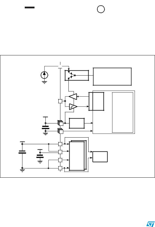
5.1.6Power supply scheme
Figure 10. Power supply scheme
VBAT 

1.8-3.6V
Power switch |
Backup circuitry (OSC32K,RTC, Wake-up logic Backup registers)
|
OUT |
shifter |
|
|
|
|
|
GP I/Os |
|
|
IO |
IN |
Level |
Logic |
|
|
|
||
|
|
|
|
|
VDD |
|
|
|
|
|
|
VDD |
|
|
|
|
|
1/2/3/4/5 |
Regulator |
|
|
|
|
|
|
|
|
5 × 100 nF |
|
VSS |
|
|
|
+ 1 × 4.7 µF |
|
1/2/3/4/5 |
|
|
VDD |
|
|
VDDA |
|
|
|
|
|
|
|
|
|
VREF |
VREF+ |
|
|
|
|
|
|
|
|
|
10 nF |
10 nF |
|
VREF- |
ADC |
Analog: |
+ 1 µF |
|
RCs, PLL, |
|||
+ 1 µF |
|
||||
|
|
|
|
... |
|
|
|
|
|
|
|
|
|
|
VSSA |
|
|
Kernel logic (CPU, Digital
& Memories)
ai14125d
Caution: In Figure 10, the 4.7 µF capacitor must be connected to VDD3.
32/86 |
Doc ID 16455 Rev 3 |