


STM32F100x4, STM32F100x6, STM32F100x8, STM32F100xB |
Electrical characteristics |
||||||
|
|
|
|
|
|
|
|
|
Table 18. |
Peripheral current consumption |
|
|
|
||
|
|
|
|
|
|
|
|
|
|
Peripheral |
Typical consumption at 25 °C(1) |
Unit |
|
||
|
|
|
|
|
|
|
|
|
|
|
TIM2 |
|
0.52 |
|
|
|
|
|
|
|
|
|
|
|
|
|
TIM3 |
|
0.46 |
|
|
|
|
|
|
|
|
|
|
|
|
|
TIM4 |
|
0.5 |
|
|
|
|
|
|
|
|
|
|
|
|
|
TIM6 |
|
0.125 |
|
|
|
|
|
|
|
|
|
|
|
|
|
TIM7 |
|
0.19 |
|
|
|
|
|
|
|
|
|
|
|
|
|
DAC |
|
0.5(2) |
|
|
|
APB1 |
|
WWDG |
|
0.13 |
|
|
|
|
|
|
|
|
|
|
|
|
|
SPI2 |
|
0.2 |
|
|
|
|
|
|
|
|
|
|
|
|
|
USART2 |
|
0.38 |
|
|
|
|
|
|
|
|
|
|
|
|
|
USART3 |
|
0.32 |
|
|
|
|
|
|
|
|
|
|
|
|
|
I2C1 |
|
0.27 |
|
|
|
|
|
|
|
|
|
|
|
|
|
I2C2 |
|
0.28 |
|
|
|
|
|
|
|
|
|
|
|
|
|
HDMI CEC |
|
0.16 |
mA |
|
|
|
|
|
|
|
|
|
|
|
|
GPIO A |
|
0.25 |
|
|
|
|
|
|
|
|
|
|
|
|
|
GPIO B |
|
0.12 |
|
|
|
|
|
|
|
|
|
|
|
|
|
GPIO C |
|
0.18 |
|
|
|
|
|
|
|
|
|
|
|
|
|
GPIO D |
|
0.15 |
|
|
|
|
|
|
|
|
|
|
|
|
|
GPIO E |
|
0.15 |
|
|
|
|
|
|
|
|
|
|
|
APB2 |
|
ADC1(3) |
|
1.15 |
|
|
|
|
SPI1 |
|
0.12 |
|
|
|
|
|
|
|
|
|
||
|
|
|
|
|
|
|
|
|
|
|
USART1 |
|
0.27 |
|
|
|
|
|
|
|
|
|
|
|
|
|
TIM1 |
|
0.63 |
|
|
|
|
|
|
|
|
|
|
|
|
|
TIM15 |
|
0.33 |
|
|
|
|
|
|
|
|
|
|
|
|
|
TIM16 |
|
0.26 |
|
|
|
|
|
|
|
|
|
|
|
|
|
TIM17 |
|
0.25 |
|
|
|
|
|
|
|
|
|
|
1.fHCLK = fAPB1 = fAPB2 = 24 MHz, default prescaler value for each peripheral.
2.Specific conditions for DAC: EN1 bit in DAC_CR register set to 1.
3.Specific conditions for ADC: fHCLK = 24 MHz, fAPB1 = fAPB2 = fHCLK, fADCCLK = fAPB2/2, ADON bit in the ADC_CR2 register is set to 1.
5.3.6External clock source characteristics
High-speed external user clock generated from an external source
The characteristics given in Table 19 result from tests performed using an high-speed external clock source, and under the ambient temperature and supply voltage conditions summarized in Table 8.
Doc ID 16455 Rev 3 |
45/86 |

Electrical characteristics |
STM32F100x4, STM32F100x6, STM32F100x8, STM32F100xB |
|||||||
|
|
|
|
|
|
|
|
|
|
Table 19. |
High-speed external user clock characteristics |
|
|
|
|||
|
|
|
|
|
|
|
|
|
|
Symbol |
|
Parameter |
Conditions |
Min |
Typ |
Max |
Unit |
|
|
|
|
|
|
|
|
|
|
fHSE_ext |
User external clock source |
|
1 |
8 |
24 |
MHz |
|
|
frequency(1) |
|
|
|||||
|
VHSEH |
OSC_IN input pin high level |
|
0.7VDD |
|
VDD |
|
|
|
(1) |
|
|
|
|
|||
|
|
voltage |
|
|
|
|
|
V |
|
VHSEL |
OSC_IN input pin low level |
|
VSS |
|
0.3VDD |
||
|
|
|
|
|||||
|
(1) |
|
|
|
|
|||
|
|
voltage |
|
|
|
|
|
|
|
tw(HSE) |
|
(1) |
|
16 |
|
|
|
|
tw(HSE) |
OSC_IN high or low time |
|
|
|
|
||
|
|
|
|
|
|
|
ns |
|
|
tr(HSE) |
|
(1) |
|
|
|
20 |
|
|
|
|
|
|
|
|||
|
tf(HSE) |
OSC_IN rise or fall time |
|
|
|
|
||
|
|
|
|
|
|
|
|
|
|
Cin(HSE) |
OSC_IN input capacitance(1) |
|
|
5 |
|
pF |
|
|
DuCy(HSE) |
Duty cycle(1) |
|
45 |
|
55 |
% |
|
|
IL |
OSC_IN Input leakage current |
VSS VIN VDD |
|
|
±1 |
µA |
|
1. Guaranteed by design, not tested in production.
Low-speed external user clock generated from an external source
The characteristics given in Table 20 result from tests performed using an low-speed external clock source, and under the ambient temperature and supply voltage conditions summarized in Table 8.
Table 20. |
Low-speed external user clock characteristics |
|
|
|
||
Symbol |
Parameter |
Conditions |
Min |
Typ |
Max |
Unit |
|
|
|
|
|
|
|
fLSE_ext |
User external clock source |
|
|
32.768 |
1000 |
kHz |
(1) |
|
|
||||
|
frequency |
|
|
|
|
|
VLSEH |
OSC32_IN input pin high level |
|
0.7VDD |
|
VDD |
|
(1) |
|
|
|
|||
|
voltage |
|
|
|
|
V |
VLSEL |
OSC32_IN input pin low level |
|
VSS |
|
0.3VDD |
|
|
|
|
||||
(1) |
|
|
|
|||
|
voltage |
|
|
|
|
|
tw(LSE) |
(1) |
|
450 |
|
|
|
tw(LSE) |
OSC32_IN high or low time |
|
|
|
|
|
|
|
|
|
|
ns |
|
tr(LSE) |
OSC32_IN rise or fall time(1) |
|
|
|
50 |
|
|
|
|
|
|||
tf(LSE) |
|
|
|
|
|
|
Cin(LSE) |
OSC32_IN input capacitance(1) |
|
|
5 |
|
pF |
DuCy(LSE) |
Duty cycle(1) |
|
30 |
|
70 |
% |
IL |
OSC32_IN Input leakage current |
VSS VIN VDD |
|
|
±1 |
µA |
1. Guaranteed by design, not tested in production.
46/86 |
Doc ID 16455 Rev 3 |
STM32F100x4, STM32F100x6, STM32F100x8, STM32F100xB Electrical characteristics
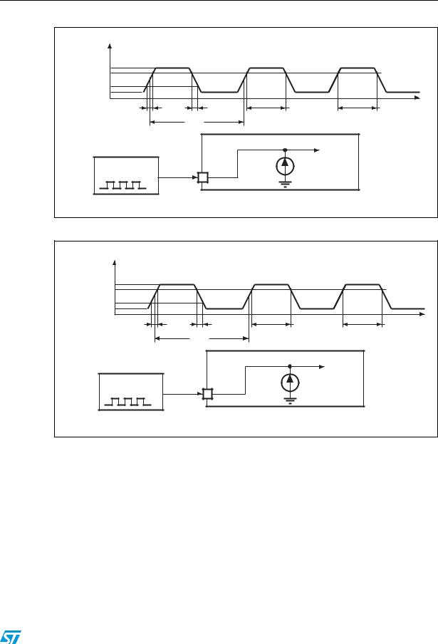
Figure 18. High-speed external clock source AC timing diagram
VHSEH |
|
|
|
|
90% |
|
|
|
|
10% |
|
|
|
|
VHSEL |
|
|
|
|
tr(HSE) |
tf(HSE) |
tW(HSE) |
tW(HSE) |
t |
|
THSE |
|
|
|
External |
fHSE_ext |
IL |
|
|
OSC _IN |
|
|
||
clock source |
|
|
|
|
|
|
STM32F10xxx |
|
|
|
|
|
ai14127b |
|
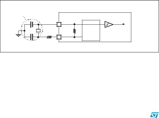
Figure 19. Low-speed external clock source AC timing diagram
VLSEH |
|
|
|
|
90% |
|
|
|
|
10% |
|
|
|
|
VLSEL |
|
|
|
|
tr(LSE) |
tf(LSE) |
tW(LSE) |
tW(LSE) |
t |
|
TLSE |
|
|
|
External |
fLSE_ext |
IL |
|
|
clock source |
OSC32_IN |
|
|
|
|
|
|
|
|
|
|
STM32F10xxx |
|
|
|
|
|
ai14140c |
|
High-speed external clock generated from a crystal/ceramic resonator
The high-speed external (HSE) clock can be supplied with a 4 to 24 MHz crystal/ceramic resonator oscillator. All the information given in this paragraph are based on characterization results obtained with typical external components specified in Table 21. In the application, the resonator and the load capacitors have to be placed as close as possible to the oscillator pins in order to minimize output distortion and startup stabilization time. Refer to the crystal resonator manufacturer for more details on the resonator characteristics (frequency, package, accuracy).
Doc ID 16455 Rev 3 |
47/86 |
Electrical characteristics |
STM32F100x4, STM32F100x6, STM32F100x8, STM32F100xB |
||||||||
|
|
|
|
|
|
|
|
||
|
Table 21. |
HSE 4-24 MHz oscillator characteristics(1)(2) |
|
|
|
|
|||
|
Symbol |
Parameter |
|
Conditions |
Min |
Typ |
Max |
Unit |
|
|
|
|
|
|
|
|
|
|
|
|
fOSC_IN |
Oscillator frequency |
|
|
4 |
8 |
24 |
MHz |
|
|
RF |
Feedback resistor |
|
|
|
|
200 |
|
k |
|
CL1 |
Recommended load capacitance |
RS = 30 |
|
|
|
|
||
|
versus equivalent serial |
|
|
30 |
|
pF |
|||
|
C (3) |
(4) |
|
|
|||||
|
L2 |
resistance of the crystal (RS) |
|
|
|
|
|
|
|
|
|
|
|
|
|
|
|
||
|
i2 |
|
|
|
VDD = 3.3 V |
|
|
|
|
|
HSE driving current |
|
VIN = VSS with 30 pF |
|
|
1 |
mA |
||
|
|
|
|
|
load |
|
|
|
|
|
|
|
|
|
|
|
|
|
|
|
gm |
Oscillator transconductance |
|
Startup |
25 |
|
|
mA/V |
|
|
tSU(HSE) |
Startup time |
|
|
VDD is stabilized |
|
2 |
|
ms |
|
(5) |
|
|
|
|
||||
|
|
|
|
|
|
|
|
|
|
1.Resonator characteristics given by the crystal/ceramic resonator manufacturer.
2.Based on characterization, not tested in production.
3.It is recommended to use high-quality external ceramic capacitors in the 5 pF to 25 pF range (typ.), designed for high-frequency applications, and selected to match the requirements of the crystal or
resonator. CL1 and CL2, are usually the same size. The crystal manufacturer typically specifies a load capacitance which is the series combination of CL1 and CL2. PCB and MCU pin capacitance must be included (10 pF can be used as a rough estimate of the combined pin and board capacitance) when sizing CL1 and CL2.
4.The relatively low value of the RF resistor offers a good protection against issues resulting from use in a humid environment, due to the induced leakage and the bias condition change. However, it is recommended to take this point into account if the MCU is used in tough humidity conditions.
5.tSU(HSE) is the startup time measured from the moment it is enabled (by software) to a stabilized 8 MHz oscillation is reached. This value is measured for a standard crystal resonator and it can vary significantly with the crystal manufacturer
Figure 20. Typical application with an 8 MHz crystal
Resonator with |
|
|
|
integrated capacitors |
|
|
|
CL1 |
|
OSC_IN |
fHSE |
|
|
||
|
8 MHz |
|
Bias |
|
RF |
controlled |
|
|
resonator |
||
|
|
gain |
|
|
|
|
|
CL2 |
REXT(1) |
OSC_OU T |
STM32F10xxx |
|
|
ai14128b
1. REXT value depends on the crystal characteristics.
Low-speed external clock generated from a crystal/ceramic resonator
The low-speed external (LSE) clock can be supplied with a 32.768 kHz crystal/ceramic resonator oscillator. All the information given in this paragraph are based on characterization results obtained with typical external components specified in Table 22. In the application, the resonator and the load capacitors have to be placed as close as possible to the oscillator pins in order to minimize output distortion and startup stabilization time. Refer to the crystal resonator manufacturer for more details on the resonator characteristics (frequency, package, accuracy).
48/86 |
Doc ID 16455 Rev 3 |

STM32F100x4, STM32F100x6, STM32F100x8, STM32F100xB |
Electrical characteristics |
|
|
|
|
Note: |
For CL1 and CL2 it is recommended to use high-quality ceramic capacitors in the 5 pF to |
|
|
15 pF range selected to match the requirements of the crystal or resonator. CL1 and CL2, are |
|
|
usually the same size. The crystal manufacturer typically specifies a load capacitance which |
|
is the series combination of CL1 and CL2.
Load capacitance CL has the following formula: CL = CL1 x CL2 / (CL1 + CL2) + Cstray where Cstray is the pin capacitance and board or trace PCB-related capacitance. Typically, it is between 2 pF and 7 pF.
Caution: To avoid exceeding the maximum value of CL1 and CL2 (15 pF) it is strongly recommended to use a resonator with a load capacitance CL 7 pF. Never use a resonator with a load capacitance of 12.5 pF.
Example: if you choose a resonator with a load capacitance of CL = 6 pF, and Cstray = 2 pF, then CL1 = CL2 = 8 pF.
Table 22. |
LSE oscillator characteristics (fLSE = 32.768 kHz)(1) |
|
|
|
|||
Symbol |
Parameter |
|
Conditions |
Min |
Typ |
Max |
Unit |
|
|
|
|
|
|
|
|
RF |
Feedback resistor |
|
|
|
5 |
|
M |
CL1 |
Recommended load capacitance |
RS = 30 K |
|
|
|
|
|
versus equivalent serial |
|
|
|
15 |
pF |
||
C (2) |
(3) |
|
|
||||
L2 |
resistance of the crystal (RS) |
|
|
|
|
|
|
|
|
|
|
|
|
|
|
I2 |
LSE driving current |
|
VDD = 3.3 V |
|
|
1.4 |
µA |
|
VIN = VSS |
|
|
||||
|
|
|
|
|
|
|
|
gm |
Oscillator transconductance |
|
|
5 |
|
|
µA/V |
(4) |
Startup time |
|
VDD is stabilized |
|
3 |
|
s |
tSU(LSE) |
|
|
|
||||
1.Based on characterization, not tested in production.
2.Refer to the note and caution paragraphs above the table.
3.The oscillator selection can be optimized in terms of supply current using an high quality resonator with small RS value for example MSIV-TIN32.768 kHz. Refer to crystal manufacturer for more details
4.tSU(LSE) is the startup time measured from the moment it is enabled (by software) to a stabilized
32.768 kHz oscillation is reached. This value is measured for a standard crystal resonator and it can vary significantly with the crystal manufacturer
Figure 21. Typical application with a 32.768 kHz crystal
Resonator with integrated capacitors
CL1 |
OSC32_IN |
fLSE |
|
|
|||
32.768 KHz |
|
Bias |
|
RF |
controlled |
||
resonator |
|||
|
gain |
||
|
|
||
CL2 |
OSC32_OU T |
STM32F10xxx |
|
|
|
ai14129b
Doc ID 16455 Rev 3 |
49/86 |