


Description |
STM32F100x4, STM32F100x6, STM32F100x8, STM32F100xB |
|
|
2 Description
The STM32F100xx value line family incorporates the high-performance ARM Cortex™-M3 32-bit RISC core operating at a 24 MHz frequency, high-speed embedded memories (Flash memory up to 128 Kbytes and SRAM up to 8 Kbytes), and an extensive range of enhanced peripherals and I/Os connected to two APB buses. All devices offer standard communication interfaces (up to two I2Cs, two SPIs, one HDMI CEC, and up to three USARTs), one 12-bit ADC, two 12-bit DACs, up to six general-purpose 16-bit timers and an advanced-control PWM timer.
The STM32F100xx lowand medium-density value line family operates in the –40 to +85 °C and –40 to +105 °C temperature ranges, from a 2.0 to 3.6 V power supply. A comprehensive set of power-saving mode allows the design of low-power applications.
The STM32F100xx value line family includes devices in three different packages ranging from 48 pins to 100 pins. Depending on the device chosen, different sets of peripherals are included, the description below gives an overview of the complete range of peripherals proposed in this family.
These features make the STM32F100xx value line microcontroller family suitable for a wide range of applications:
●Application control and user interface
●Medical and handheld equipment
●PC peripherals, gaming and GPS platforms
●Industrial applications: PLC, inverters, printers, and scanners
●Alarm systems, Video intercom, and HVAC
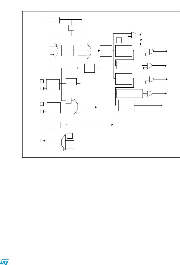
Figure 1 shows the general block diagram of the device family.
10/86 |
Doc ID 16455 Rev 3 |
STM32F100x4, STM32F100x6, STM32F100x8, STM32F100xB |
Description |
|
|
2.1Device overview
Table 2. |
STM32F100xx features and peripheral counts |
|
|
|
|
|
|
|
|
|
|
|||||||||
|
Peripheral |
STM32F100Cx |
|
|
|
STM32F100Rx |
STM32F100Vx |
|||||||||||||
|
|
|
|
|
|
|
|
|
|
|
|
|
|
|
|
|
|
|
||
Flash - Kbytes |
16 |
|
32 |
|
64 |
|
128 |
|
16 |
|
32 |
|
64 |
|
128 |
64 |
|
128 |
||
|
|
|
|
|
|
|
|
|
|
|
|
|
|
|
|
|
|
|
||
SRAM - Kbytes |
4 |
|
4 |
|
8 |
|
8 |
|
4 |
|
4 |
|
8 |
|
8 |
8 |
|
8 |
||
|
|
|
|
|
|
|
|
|
|
|
|
|
|
|
|
|
|
|
|
|
Timers |
|
Advanced-control |
1 |
|
|
1 |
|
|
|
1 |
|
|
1 |
|
1 |
|||||
|
|
|
|
|
|
|
|
|
|
|
|
|
|
|
|
|
|
|
|
|
|
General-purpose |
5(1) |
|
|
6 |
|
|
|
5(1) |
|
|
6 |
|
6 |
||||||
|
|
|
|
|
|
|
|
|
|
|||||||||||
|
|
SPI |
1(2) |
|
|
2 |
|
|
|
1(2) |
|
|
2 |
|
2 |
|||||
Communication |
I2C |
1(3) |
|
|
2 |
|
|
|
1(3) |
|
|
2 |
|
2 |
||||||
interfaces |
|
USART |
2(4) |
|
|
3 |
|
|
|
2(4) |
|
|
3 |
|
3 |
|||||
|
|
CEC |
|
|
|
|
|
|
|
|
|
1 |
|
|
|
|
|
|
|
|
|
|
|
|
|
|
|
|
|
|
|
|
|
|
|
|
|
|
|
|
|
12-bit synchronized ADC |
|
|
|
1 |
|
|
|
|
1 |
|
|
|
|
1 |
||||||
number of channels |
|
10 channels |
|
|
|
|
16 channels |
|
|
16 channels |
||||||||||
|
|
|
|
|
|
|
|
|
|
|
|
|
|
|
|
|
||||
GPIOs |
|
|
|
|
|
37 |
|
|
|
|
51 |
|
|
|
|
80 |
||||
|
|
|
|
|
|
|
|
|
|
|
|
|
|
|
|
|
|
|
|
|
12-bit DAC |
|
|
|
|
|
|
|
|
|
|
|
2 |
|
|
|
|
|
|
|
|
Number of channels |
|
|
|
|
|
|
|
|
|
2 |
|
|
|
|
|
|
|
|||
|
|
|
|
|
|
|
|
|
|
|
|
|
|
|
|
|
||||
CPU frequency |
|
|
|
|
|
|
|
|
|
24 MHz |
|
|
|
|
|
|
||||
|
|
|
|
|
|
|
|
|
|
|
|
|
|
|
|
|||||
Operating voltage |
|
|
|
|
|
|
|
|
2.0 to 3.6 V |
|
|
|
|
|
|
|||||
|
|
|
|
|||||||||||||||||
Operating temperatures |
Ambient operating temperature: –40 to +85 °C /–40 to +105 °C (see Table 8) |
|||||||||||||||||||
|
|
|
Junction temperature: –40 to +125 °C (see Table 8) |
|
|
|||||||||||||||
|
|
|
|
|
|
|
|
|||||||||||||
|
|
|
|
|
|
|
|
|
|
|
|
|
|
|||||||
Packages |
|
|
|
|
LQFP48 |
|
|
LQFP64, TFBGA64 |
LQFP100 |
|||||||||||
|
|
|
|
|
|
|
|
|
|
|
|
|
|
|
|
|
|
|
|
|
1.TIM4 not present.
2.SPI2 is not present.
3.I2C2 is not present.
4.USART3 is not present.
Doc ID 16455 Rev 3 |
11/86 |

Description |
STM32F100x4, STM32F100x6, STM32F100x8, STM32F100xB |
|
|
Figure 1. STM32F100xx value line block diagram
42!#%#,+ |
|
|
|
|
|
4RACE |
|
|
|
|
|
|
|
|
42!#%$; = |
40)* |
|
|
PBUS |
|
|
|
|
|
6$$ |
|
0OWER |
|
|
|
%4- |
|
CONTROLLER |
|
|
|
|
|
||||||
AS !& |
|
|
|
|
|
|
|
|
|
6$$ 66TO 6 |
||||
|
TRACE TRIGGER |
|
|
|
|
|
|
|
|
6OLTAGE REG |
||||
|
37*4!' |
|
|
|
|
|
|
|
|
|||||
.*4234 |
|
|
|
|
|
OBL |
|
|
|
|
66TO 6 |
633 |
||
|
|
|
|
|
|
|
&LASHA H+" |
|
|
|||||
*4$) |
|
|
|
)BUS |
|
|
|
|
|
|
|
|||
#ORTEX - #05 |
|
&LASH INTERFACE |
|
|
|
|
|
|||||||
*4#+ 37#,+ |
|
|
|
BIT |
|
|
6$$ |
|
||||||
*4-3 37$)/ |
|
|
|
|
|
|
|
|
|
|
|
|||
|
|
|
|
|
|
|
|
|
|
|
|
|||
*4$/ |
|
|
|
$BUS |
|
|
|
|
|
|
|
|
||
FMAX -(Z |
|
|
|
|
|
|
0/2 |
3UPPLY |
|
|||||
AS !& |
|
|
|
|
|
|
|
.234 |
||||||
|
|
|
|
|
32!-! |
|
SUPERVISION |
|||||||
|
|
|
|
|
|
|
|
|
|
2ESET |
|
|
6$$! |
|
|
|
|
|
3YSTEM |
"USUMATRIX |
|
|
|
+" |
6$$! |
)NT |
0/2/ 0$2 |
||
|
|
|
|
|
|
|
633! |
|||||||
|
|
|
|
|
|
|
|
|
|
|
||||
|
.6)# |
|
|
|
|
|
|
2# (3 |
|
|
06$ |
|
||
|
|
'0 $-! |
|
|
|
|
|
2# ,3 |
6$$! |
|
||||
|
|
|
|
|
|
|
|
|
|
|||||
|
|
|
|
|
|
|
|
|
|
|
|
|
6$$ |
/3#?). |
|
|
CHANNELS |
|
|
|
|
|
|
|
|
|
|
||
|
|
|
|
|
|
|
|
|
|
|
84!, /3# |
/3#?/54 |
||
|
|
|
|
|
|
|
|
|
|
0,, |
|
|
||
|
|
|
|
|
|
|
|
|
|
|
|
-(Z |
|
|
|
|
|
|
|
|
|
|
|
|
|
|
|
|
|
|
|
|
|
|
|
|
|
|
2ESETS |
0#,+ |
|
)7$' |
|
|
|
|
|
|
|
|
|
|
|
|
|
|
|
||
|
|
|
|
|
|
|
-(Z |
|
CLOCK |
0#,+ |
|
3TANDBY |
|
|
|
|
|
|
|
|
|
|
CONTROL |
(#,+ |
|
INTERFACE |
6"!4 6 TO 6 |
||
|
|
|
|
|
|
|
|
|
,+ |
|
|
|
||
|
%84)4 |
|
|
|
|
|
|
|
|
6"!4 |
|
|||
!& |
|
|
|
|
|
|
|
|
|
|
|
|||
7+50 |
|
|
|
|
|
|
|
|
|
/3# ?). |
||||
|
|
|
|
|
MAX |
|
|
|
|
|
|
|||
|
|
|
|
|
|
|
|
|
|
|
84!, K(Z |
|||
|
'0)/ PORTT! |
|
|
|
|
|
|
|
/3# ?/54 |
|||||
0!; = |
|
|
|
& |
|
|
|
|
|
|
||||
|
|
|
!("( |
|
|
|
|
|
"ACKUP |
|
||||
|
|
|
|
|
|
|
|
|
|
24# |
4!- 0%2 24# |
|||
0"; = |
'0)/ PORTT" |
|
|
|
|
|
|
!75 |
REGISTER |
|||||
|
|
|
|
|
|
!,!2- /54 |
||||||||
|
|
|
|
|
|
|
|
|
|
|||||
|
|
|
|
|
|
|
|
|
|
|
"ACKUPUINTERFACE |
|
||
0#; = |
'0)/ PORTT# |
|
|
|
|
|
|
|
|
|
|
CHANNELS |
||
|
|
|
|
|
|
!(" |
|
!(" |
|
|
4)- |
|||
0$; = |
|
|
|
|
|
|
|
|
AS !& |
|||||
'0)/ PORTT$ |
|
|
|
|
|
|
|
|||||||
|
|
!0" |
|
!0" |
|
|
|
|
CHANNELS |
|||||
|
|
|
|
|
|
|
|
|
|
|
|
4)- |
||
0%; = |
|
|
|
|
|
|
|
|
|
|
|
AS !& |
||
'0)/ PORTT% |
|
|
|
|
|
|
|
|
|
|
||||
|
|
|
|
|
|
|
|
|
|
|
||||
|
|
|
|
|
|
|
|
|
|
|
(Z |
4)- |
CHANNELS |
|
CHANNELS COMPL |
|
|
|
|
|
|
|
|
|
|
|
|
AS !& |
|
CHANNELNANDE"+). |
4)- |
|
|
|
|
|
|
|
|
- |
|
|
28 48 #43 243 |
|
|
|
|
|
|
|
|
|
|
53!24 |
|||||
AS !& |
|
|
|
|
|
|
|
|
|
|
||||
|
|
|
|
|
|
|
|
|
|
#+ ASA!& |
||||
|
|
|
|
|
|
|
|
|
|
|
|
|
|
|
CHANNEL COMPL |
|
|
|
|
|
|
|
|
|
|
|
|
|
|
|
|
|
|
|
|
|
|
|
|
MAX |
53!24 |
28 48 #43 243 |
||
CHANNELNANDE"+). |
4)- |
|
|
|
|
|
|
|
|
|||||
AS !& |
|
|
|
|
|
|
|
|
|
|
& |
|
|
#+ AS !& |
|
|
|
|
|
|
|
|
|
|
|
|
|
|
|
|
|
|
|
|
|
|
|
|
|
!0" |
|
|
|
|
CHANNEL COMPL |
|
|
|
|
(Z |
|
|
|
|
|
30) |
-/3) 3-)3/ |
||
4)- |
|
|
|
|
|
|
|
3#+ .33 AS.!& |
||||||
CHANNELNANDE"+). |
|
|
|
|
- |
|
|
|
|
|
|
|
|
|
AS !& |
|
|
|
|
|
|
|
|
|
|
|
|
|
|
|
|
|
|
|
|
|
|
|
|
|
($-) #%# |
($-) #%# AS !& |
||
CHANNELS COMPL |
|
|
|
|
|
|
|
|
|
|
||||
|
|
|
|
|
|
|
|
|
|
|
|
|
||
CHANNELS %42%AND |
4)- |
|
|
MAX |
|
|
|
|
|
|
|
|
|
|
"+). AS.!& |
|
|
|
|
|
|
|
|
|
|
|
|
|
|
|
|
|
|
& |
|
|
|
|
|
|
) # |
3#, 3$! 3-"!3AS !& |
||
|
|
|
|
|
|
|
|
|
|
|
||||
-/3) 3-)3/ |
30) |
|
|
!0" |
|
|
|
|
|
|
) # |
|
||
3#+ .33 AS.!& |
|
|
|
|
|
77$' |
|
|
3#, 3$! 3-"!3AS !& |
|||||
28 48 #43 243 |
|
|
|
|
|
|
|
|
|
|
|
|
|
|
53!24 |
|
|
|
|
|
|
|
|
|
|
|
|
||
#+ AS !& |
|
|
|
|
|
|
|
|
|
|
|
|
||
|
|
|
|
|
|
|
|
|
|
|
|
|
|
|
|
4EMP SENSOR |
|
|
|
|
|
|
4)- |
|
)& |
BIT $!# |
$!# ?/545AS !& |
||
|
|
|
|
|
|
|
|
|
|
|
)& |
|
|
|
!$# CHANNELS |
BIT !$# |
)& |
|
|
|
|
|
4)- |
|
|
BIT $!# |
$!# ?/54 AS !& |
||
!$#?).X |
|
|
|
|
|
|
|
|
|
|
|
|
|
|
62%& |
|
|
|
|
|
|
|
|
|
|
|
|
6$$! |
|
62%&n |
6$$! |
|
|
|
|
|
|
|
|
|
|
|
||
|
|
|
|
|
|
|
|
|
|
|
|
|||
|
|
|
|
|
|
|
|
|
|
|
|
|
|
AI B |
1.Peripherals not present in low-density value line devices.
2.AF = alternate function on I/O port pin.
3.TA = –40 °C to +85 °C (junction temperature up to 105 °C) or TA = –40 °C to +105 °C (junction temperature up to 125 °C).
12/86 |
Doc ID 16455 Rev 3 |
STM32F100x4, STM32F100x6, STM32F100x8, STM32F100xB |
|
|
|
|
|
Description |
|||||
Figure 2. |
Clock tree |
|
|
|
|
|
|
|
|
|
|
|
-(Z |
(3) |
|
|
|
|
|
|
|
|
|
|
(3) 2# |
|
|
|
|
|
|
|
|
|
|
|
|
|
|
|
|
|
|
|
(#,+ |
|
|
|
|
|
|
|
|
-(Z MAX |
|
|
|
|
|
|
|
|
|
|
|
|
|
TO !(" BUS CORE |
|||
|
|
|
|
|
|
|
|
|
|||
|
|
|
|
|
|
#LOCK |
|
|
MEMORY AND $-! |
||
|
|
|
|
|
|
%NABLE |
|
|
TO #ORTEXX3YSTEM TIMER |
||
|
0,,32# |
|
|
37 |
|
|
|
|
|||
|
0,,-5, |
|
|
|
|
|
,+ #ORTEX |
||||
|
|
|
|
|
|
|
|||||
|
|
X |
(3) |
393#,+ |
!(" |
!0" |
|
|
FREE RUNNING CLOCK |
||
|
|
|
|
|
|
|
|||||
|
|
|
-(ZZMAX |
|
0#,+ |
||||||
|
|
X X X |
0,,#,+ |
-(Z |
0RESCALER |
0RESCALER |
|
||||
|
|
|
|
|
|
TO !0" |
|||||
|
|
0,, |
|
|
|
|
|
|
|||
|
|
|
MAX |
0ERIPHERAL #LOCK |
PERIPHERALS |
||||||
|
|
|
(3% |
|
|
||||||
|
|
|
|
|
|
%NABLE |
|
|
|||
|
|
|
|
|
|
|
|
|
|||
|
|
|
|
|
|
4)- |
|
|
|
TO 4)- AND |
|
|
|
|
|
|
|
)F !0" PRESCALER |
X |
|
|||
|
|
|
|
|
|
|
4)-X#,+ |
||||
|
|
|
|
#33 |
|
|
ELSE SX |
|
|||
|
|
|
|
|
|
0ERIPHERAL #LOCK |
|||||
|
|
|
|
|
|
|
|
|
|||
|
|
|
|
|
|
|
|
|
%NABLE |
|
|
|
|
02%$)6 |
|
|
!0" |
-(Z MAX |
|
0#,+ |
|||
|
|
|
|
|
0RESCALER |
|
|||||
/3#?/54 |
|
|
|
|
|
|
|
PERIPHERALSLTO !0" |
|||
|
|
|
|
|
|
|
|
||||
-(Z |
|
|
|
0ERIPHERAL #LOCK |
|||||||
|
|
|
|
|
|||||||
|
|
|
|
|
|
|
|
||||
/3#?). |
(3%%/3# |
|
|
|
|
|
%NABLE |
TO 4)- 4)- |
|||
|
|
|
|
|
4)- TIMERS |
|
|||||
|
|
|
|
|
|
|
4)- AND 4)- |
||||
|
|
|
|
|
|
)F !0" PRESCALER |
X |
||||
|
|
|
|
|
|
4)-X#,+ |
|||||
|
|
|
|
|
|
|
ELSE X |
||||
|
|
|
|
|
|
|
|
|
0ERIPHERAL #LOCK |
||
|
|
|
|
|
!$# |
|
|
%NABLE |
|
|
|
/3# ?). |
|
|
|
TO 24# |
|
|
|
|
|
TO !$# |
|
,3% /3# |
,3% |
|
|
0RESCALER |
!$##,+ -(Z MAX |
||||||
|
|
|
|||||||||
|
K(Z |
|
24##,+ |
|
|
||||||
/3# ?/54 |
|
|
|
|
|
|
|
||||
|
|
|
|
|
|
|
|
|
|
|
|
|
|
24#3%,; == |
|
|
|
|
|
|
|
|
|
|
,3) 2# |
,3) |
TO INDEPENDENT WATCHDOG )7$' |
|
|
|
|
|
|
||
|
|
|
|
|
|
|
|
|
|
||
|
K(Z |
|
|
)7$'#,+ |
|
|
|
|
|
|
|
|
-AIN |
|
0,,#,+ |
|
|
,EGEND |
|
|
|
|
|
|
|
|
|
|
|
|
|
|
|||
-#// |
CLOCK OUT PUT |
|
|
|
|
(3% (IGH SPEED EXTERNAL CLOCK SIGNAL |
|||||
|
|
(3) |
|
|
(3) (IGH SPEED INTERNAL CLOCKKSIGNAL |
||||||
|
|
|
(3% |
|
|
,3) ,OW SPEED INTERNAL CLOCKKSIGNAL |
|||||
|
|
|
393#,+ |
|
|
,3%% ,OWWSPEED EXTERNAL CLOCKKSIGNAL |
|||||
|
-#/ |
|
|
|
|
|
|
|
|
AI |
|
|
|
|
|
|
|
|
|
|
|
|
|
4. To have an ADC conversion time of 1.2 µs, APB2 must be at 24 MHz.
Doc ID 16455 Rev 3 |
13/86 |