

Memory mapping |
STM32F100x4, STM32F100x6, STM32F100x8, STM32F100xB |
|
|
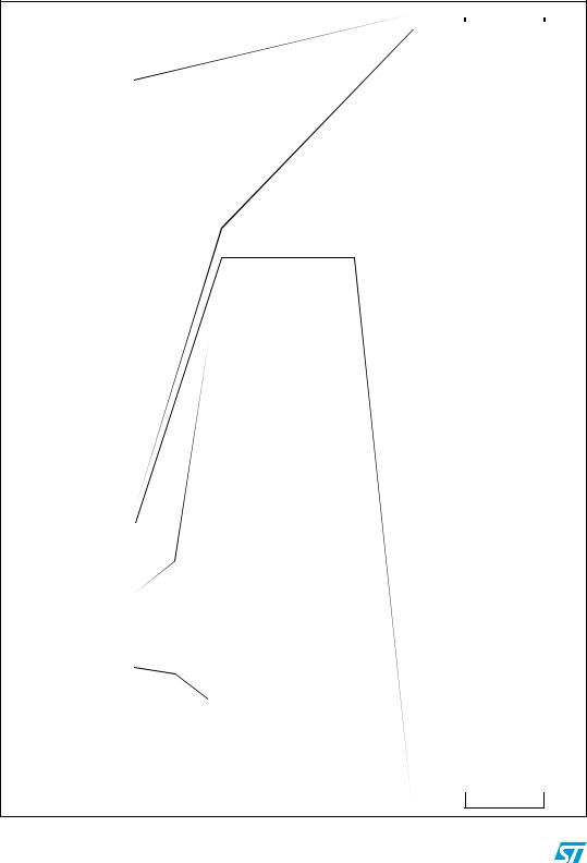
4 Memory mapping
The memory map is shown in Figure 7.
Figure 7. Memory map
0xFFFF FFFF |
|
|
|
|
||
7 |
|
|
|
|
|
|
0xE010 0000 |
|
|
|
|
||
Cortex-M3 internal |
|
|
||||
0xE000 0000 |
peripherals |
|
|
|||
6 |
|
|
|
|
|
|
0xC000 0000 |
|
|
|
|
||
5 |
|
|
|
|
|
|
0xA000 0000 |
|
|
|
|
||
4 |
|
|
|
|
0x1FFF FFFF |
|
|
|
|
|
reserved |
||
|
|
|
|
|
0x1FFF F80F |
|
0x8000 0000 |
|
|
Option Bytes |
|||
|
|
|
||||
|
|
|
|
|
0x1FFF F800 |
|
|
|
|
|
|
|
|
3 |
|
|
|
|
|
System memory |
0x6000 0000 |
|
|
0x1FFF F000 |
|
||
|
|
|
|
|||
2 |
|
|
|
|
|
|
|
|
|
|
|
|
reserved |
0x4000 0000 |
Peripherals |
|
|
|||
|
|
|
|
|||
1 |
|
|
|
|
|
|
|
|
|
|
|
|
|
0x2000 0000 |
SRAM |
|
|
|||
|
|
0x0801 FFFF |
|
|||
|
|
|
|
|
|
|
0 |
|
|
|
|
|
Flash memory |
0x0000 0000 |
|
|
|
0x0800 0000 |
|
|
|
|
|
|
|||
|
|
|
|
Aliased to Flash or |
||
|
|
|
|
|||
|
|
|
|
|
|
|
|
|
|
|
|
|
system memory |
|
|
|
|
|
|
depending on |
|
|
|
|
|
0x0000 0000 |
BOOT pins |
|
|
|
|
Reserved |
|
|
|
|
|
|
|||
0xFFFF FFFF |
APB memory space |
|||
|
|
|||
0x4002 |
3400 |
|
reserved |
|
|
|
|
||
0x4002 |
3000 |
|
CRC |
|
|
|
|
||
0x4002 |
2400 |
|
reserved |
|
0x4002 |
2000 |
|
Flash interface |
|
0x4002 |
1400 |
|
reserved |
|
0x4002 |
1000 |
|
RCC |
|
|
|
|
||
0x4002 |
0400 |
|
reserved |
|
0x4002 |
0000 |
|
DMA |
|
0x4001 4C00 |
reserved |
|
||
|
|
|||
0x4001 |
4800 |
|
TIM17 |
|
|
|
|
||
0x4001 |
4400 |
|
TIM16 |
|
|
|
|
||
0x4001 |
4000 |
|
TIM15 |
|
|
|
|
||
0x4001 |
3C00 |
reserved |
|
|
|
|
|||
0x4001 |
3800 |
|
USART1 |
|
|
|
|
||
0x4001 |
3400 |
|
reserved |
|
0x4001 |
3000 |
|
SPI1 |
|
|
|
|
||
0x4001 |
2C00 |
TIM1 |
|
|
|
|
|||
0x4001 |
2800 |
|
reserved |
|
0x4001 |
2400 |
|
ADC1 |
|
|
|
|
||
0x4001 |
1C00 |
reserved |
|
|
0x4001 |
1800 |
|
Port E |
|
|
|
|
||
0x4001 |
1400 |
|
Port D |
|
|
|
|
||
0x4001 |
1000 |
|
Port C |
|
|
|
|
||
0x4001 |
0C00 |
Port B |
|
|
|
|
|||
0x4001 |
0800 |
|
Port A |
|
|
|
|
||
0x4001 |
0400 |
|
EXTI |
|
|
|
|
||
0x4001 |
0000 |
|
AFIO |
|
|
|
|
||
0x4000 7C00 |
reserved |
|
||
0x4000 |
7800 |
|
CEC |
|
|
|
|
||
0x4000 |
7400 |
|
DAC |
|
|
|
|
||
0x4000 |
7000 |
|
PWR |
|
|
|
|
||
0x4000 |
6C00 |
BKP |
|
|
|
|
|||
0x4000 |
5C00 |
|
I2C2 |
|
|
|
|||
|
|
|
||
0x4000 |
5800 |
|
reserved |
|
|
|
|
|
|
0x4000 |
5400 |
|
I2C1 |
|
|
|
|
||
0x4000 |
4C00 |
reserved |
|
|
USART3 |
|
|||
0x4000 |
4800 |
|
|
|
|
|
|
||
0x4000 |
4400 |
|
USART2 |
|
|
|
|
||
0x4000 |
3C00 |
reserved |
|
|
|
|
|||
0x4000 |
3800 |
|
SPI2 |
|
|
|
|
||
0x4000 |
3400 |
|
reserved |
|
0x4000 |
3000 |
|
IWDG |
|
0x4000 |
2C00 |
WWDG |
|
|
0x4000 |
2800 |
|
RTC |
|
0x4000 |
1800 |
|
reserved |
|
0x4000 |
1400 |
|
TIM7 |
|
|
|
|
||
0x4000 |
1000 |
|
TIM6 |
|
|
|
|
||
0x4000 0C00 |
reserved |
|
||
0x4000 |
0800 |
|
TIM4 |
|
|
|
|
||
0x4000 |
0400 |
|
TIM3 |
|
|
|
|
||
0x4000 |
0000 |
|
TIM2 |
|
|
|
|
||
ai17156
30/86 |
Doc ID 16455 Rev 3 |