

Electrical characteristics |
STM32F100x4, STM32F100x6, STM32F100x8, STM32F100xB |
||||||||||||
|
|
|
|
|
|
|
|
|
|
|
|
|
|
|
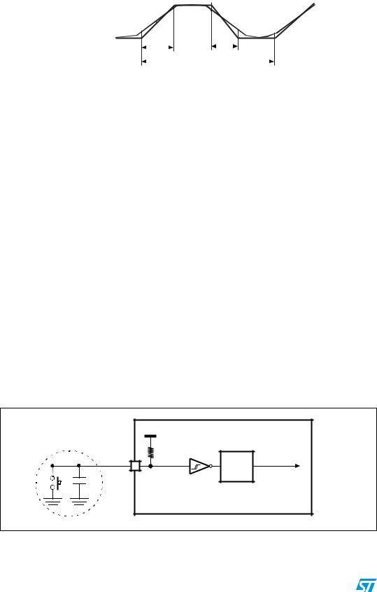
Figure 26. I/O AC characteristics definition |
|
|
|
|
|
|
|
|||||
|
|
|
|
|
|
|
|
||||||
|
|
90% |
10% |
|
|
|
|
||||||
|
|
|
|
|
|
|
|
|
|
50% |
|
|
|
|
|
tr(I O)out |
|
|
|
|
|
|
|
90% |
|
||
|
|
|
|
|
|
|
|
||||||
|
EXTERNAL |
|
|
|
|
|
|
|
|
tr(I O)out |
|||
|
|
|
|
|
|
|
|
|
|||||
|
|
|
|
||||||||||
|
OUTPUT |
|
|
|
|
|
T |
|
|
|
|
|
|
|
ON 50pF |
|
|
|
|
|
|
|
|
|
|
||
|
|
|
|
|
|
|
|
|
|
||||
|
|
|
|
|
|
|
|
|
|
|
|
|
|
|
Maximum frequency is achieved if (tr + tf) 2/3)T and if the duty cycle is (45-55%) |
||||||||||||
|
|
|
|
when loaded by 50pF |
|||||||||
|
|
|
|
|
|
|
|
|
|
|
|
|
ai14131 |
|
|
|
|
|
|
|
|
|
|
|
|
|
|
5.3.13NRST pin characteristics
The NRST pin input driver uses CMOS technology. It is connected to a permanent pull-up resistor, RPU (see Table 33).
Unless otherwise specified, the parameters given in Table 36 are derived from tests performed under the ambient temperature and VDD supply voltage conditions summarized in Table 8.
Table 36. |
NRST pin characteristics |
|
|
|
|
|
|
|
|
|
Symbol |
|
Parameter |
Conditions |
Min |
Typ |
Max |
Unit |
|||
|
|
|
|
|
|
|
|
|
|
|
(1) |
|
NRST Input low level voltage |
|
|
|
|
–0.5 |
|
0.8 |
|
VIL(NRST) |
|
|
|
|
|
|
V |
|||
(1) |
|
NRST Input high level voltage |
|
|
|
|
2 |
|
VDD+0.5 |
|
|
|
|
|
|
|
|
||||
VIH(NRST) |
|
|
|
|
|
|
|
|||
Vhys(NRST) |
|
NRST Schmitt trigger voltage |
|
|
|
|
|
200 |
|
mV |
|
hysteresis |
|
|
|
|
|
|
|||
R |
|
Weak pull-up equivalent resistor(2) |
V |
IN |
V |
SS |
30 |
40 |
50 |
k |
PU |
|
|
|
|
|
|
|
|
||
(1) |
|
NRST Input filtered pulse |
|
|
|
|
|
|
100 |
ns |
VF(NRST) |
|
|
|
|
|
|
|
|||
VNF(NRST)(1) |
|
NRST Input not filtered pulse |
|
|
|
|
300 |
|
|
ns |
1.Guaranteed by design, not tested in production.
2.The pull-up is designed with a true resistance in series with a switchable PMOS. This PMOS contribution to the series resistance must be minimum (~10% order).
Figure 27. Recommended NRST pin protection
%XTERNAL |
6$$ |
|
|
|
|
||
RESETSCIRCUIT |
205 |
|
|
.234 |
)NTERNALARESET |
||
|
|||
|
|
&ILTER |
|
& |
|
|
34-& X
AI D
1.The reset network protects the device against parasitic resets.
2.The user must ensure that the level on the NRST pin can go below the VIL(NRST) max level specified in Table 36. Otherwise the reset will not be taken into account by the device.
60/86 |
Doc ID 16455 Rev 3 |
STM32F100x4, STM32F100x6, STM32F100x8, STM32F100xB |
Electrical characteristics |
|
|
5.3.14TIMx characteristics
The parameters given in Table 37 are guaranteed by design.
Refer to Section 5.3.12: I/O port characteristics for details on the input/output alternate function characteristics (output compare, input capture, external clock, PWM output).
Table 37. |
TIMx characteristics |
|
|
|
|
|
Symbol |
Parameter |
Conditions(1) |
Min |
Max |
Unit |
|
|
|
|
|
|
|
|
tres(TIM) |
Timer resolution time |
|
1 |
|
tTIMxCLK |
|
fTIMxCLK = 24 MHz |
41.7 |
|
ns |
|||
|
|
|
||||
fEXT |
Timer external clock |
|
0 |
fTIMxCLK/2 |
MHz |
|
frequency on CHx(2) |
fTIMxCLK = 24 MHz |
0 |
12 |
MHz |
||
|
||||||
ResTIM |
Timer resolution |
|
|
16 |
bit |
|
|
|
|
|
|
|
|
tCOUNTER |
16-bit counter clock period |
|
1 |
65536 |
tTIMxCLK |
|
when the internal clock is |
|
|
|
|
||
fTIMxCLK = 24 MHz |
|
2730 |
µs |
|||
|
selected |
|
||||
|
|
|
|
|
|
|
tMAX_COUNT |
Maximum possible count |
|
|
65536 × 65536 |
tTIMxCLK |
|
fTIMxCLK = 24 MHz |
|
178 |
s |
|||
|
|
|
1.TIMx is used as a general term to refer to the TIM1, TIM2, TIM3, TIM4, TIM15, TIM16 and TIM17 timers.
2.CHx is used as a general term to refer to CH1 to CH4 for TIM1, TIM2, TIM3 and TIM4, to the CH1 to CH2 for TIM15, and to CH1 for TIM16 and TIM17.
5.3.15Communications interfaces
I2C interface characteristics
Unless otherwise specified, the parameters given in Table 38 are derived from tests performed under the ambient temperature, fPCLK1 frequency and VDD supply voltage conditions summarized in Table 8.
The STM32F100xx value line I2C interface meets the requirements of the standard I2C communication protocol with the following restrictions: the I/O pins SDA and SCL are mapped to are not “true” open-drain. When configured as open-drain, the PMOS connected between the I/O pin and VDD is disabled, but is still present.
The I2C characteristics are described in Table 38. Refer also to Section 5.3.12: I/O port characteristics for more details on the input/output alternate function characteristics (SDA and SCL).
Doc ID 16455 Rev 3 |
61/86 |

Electrical characteristics |
STM32F100x4, STM32F100x6, STM32F100x8, STM32F100xB |
|||||||
|
|
|
|
|
|
|
|
|
|
Table 38. |
I2C characteristics |
|
|
|
|
|
|
|
Symbol |
|
Parameter |
Standard mode I2C(1) |
Fast mode I2C(1)(2) |
Unit |
||
|
|
|
|
|
|
|||
|
|
Min |
Max |
Min |
Max |
|||
|
|
|
|
|
||||
|
|
|
|
|
|
|
|
|
|
tw(SCLL) |
SCL clock low time |
4.7 |
|
1.3 |
|
µs |
|
|
tw(SCLH) |
SCL clock high time |
4.0 |
|
0.6 |
|
||
|
|
|
|
|||||
|
tsu(SDA) |
SDA setup time |
250 |
|
100 |
|
|
|
|
th(SDA) |
SDA data hold time |
0(3) |
|
0(4) |
900(3) |
|
|
|
tr(SDA) |
SDA and SCL rise time |
|
1000 |
|
300 |
ns |
|
|
tr(SCL) |
|
|
|
||||
|
|
|
|
|
|
|
|
|
|
tf(SDA) |
SDA and SCL fall time |
|
300 |
|
300 |
|
|
|
tf(SCL) |
|
|
|
|
|
|
|
|
th(STA) |
Start condition hold time |
4.0 |
|
0.6 |
|
|
|
|
tsu(STA) |
Repeated Start condition setup |
4.7 |
|
0.6 |
|
µs |
|
|
|
|
|
|||||
|
time |
|
|
|
|
|||
|
tsu(STO) |
Stop condition setup time |
4.0 |
|
0.6 |
|
µs |
|
|
tw(STO:STA) |
Stop to Start condition time (bus |
4.7 |
|
1.3 |
|
µs |
|
|
free) |
|
|
|
||||
|
Cb |
Capacitive load for each bus line |
|
400 |
|
400 |
pF |
|
1.Guaranteed by design, not tested in production.
2.fPCLK1 must be higher than 2 MHz to achieve standard mode I2C frequencies. It must be higher than 4 MHz to achieve fast mode I2C frequencies. It must be a multiple of 10 MHz to reach the 400 kHz maximum I2C fast mode clock.
3.The maximum hold time of the Start condition only has to be met if the interface does not stretch the low period of SCL signal.
4.The device must internally provide a hold time of at least 300 ns for the SDA signal in order to bridge the undefined region of the falling edge of SCL.
62/86 |
Doc ID 16455 Rev 3 |
STM32F100x4, STM32F100x6, STM32F100x8, STM32F100xB |
Electrical characteristics |
|
|
Figure 28. I2C bus AC waveforms and measurement circuit(1)
6$$ 6$$
KΩ |
KΩ |
Ω |
|
|
)£#£BUS |
Ω |
34-& X
3$!
3#,
|
|
|
|
|
|
|
|
|
|
|
|
|
|
|
|
|
|
|
3TARTTREPEATED |
||||
|
|
3TART |
|
|
|
|
|
|
|
|
|
|
|
|
|
|
|
||||||
|
|
|
|
|
|
|
|
|
|
|
|
|
|
|
|
|
|
TSU 34! |
|
|
|
|
3TART |
3$! |
|
|
|
|
|
|
|
|
|
|
|
|
|
|
|
|
|
|
|
|
|
|
|
|
|
|
|
|
|
|
|
|
|
|
|
|
|
|
|
|
|
|
|
|
|
||
|
|
|
|
|
|
|
|
|
|
|
|
|
|
|
|
|
|
|
|
|
|
|
|
TF 3$! |
|
|
|
|
|
|
|
|
TR 3$! |
|
|
TSU 3$! |
|
|
|
||||||||
|
|
|
|
|
|
|
|
|
|
|
TSU 34/ 34! |
||||||||||||
|
|
|
|
|
|
|
|
||||||||||||||||
|
|
|
|
|
|
|
|
|
|
|
|
|
|
|
|
|
|
|
3TOP |
|
|
||
3#, |
|
|
|
|
TH 34! |
|
|
TW 3#,, |
|
|
|
|
|
TH 3$! |
|
|
|
||||||
|
|
|
|
|
|
|
|
|
|
|
|||||||||||||
|
|
|
|
|
|
|
|
|
|
|
|
|
|
|
|
|
|
|
|
|
|
|
|
TW 3#,( |
|
|
|
TR 3#, |
|
|
|
|
|
TF 3#, |
|
|
TSU 34/ |
||||||||||
|
|
|
|
|
|
|
|
|
|
||||||||||||||
AI D
1. Measurement points are done at CMOS levels: 0.3VDD and 0.7VDD.
Table 39. SCL frequency (fPCLK1= 24 MHz, VDD = 3.3 V)(1)(2)
fSCL (kHz)(3) |
I2C_CCR value |
|
|
||
RP = 4.7 k |
||
|
||
|
|
|
400 |
0x8011 |
|
|
|
|
300 |
0x8016 |
|
|
|
|
200 |
0x8021 |
|
|
|
|
100 |
0x0064 |
|
|
|
|
50 |
0x00C8 |
|
|
|
|
20 |
0x01F4 |
|
|
|
1.RP = External pull-up resistance, fSCL = I2C speed,
2.For speeds around 400 kHz, the tolerance on the achieved speed is of 2%. For other speed ranges, the tolerance on the achieved speed 1%. These variations depend on the accuracy of the external components used to design the application.
3.Guaranteed by design, not tested in production.
Doc ID 16455 Rev 3 |
63/86 |

Electrical characteristics |
STM32F100x4, STM32F100x6, STM32F100x8, STM32F100xB |
|
|
SPI interface characteristics
Unless otherwise specified, the parameters given in Table 40 are derived from tests performed under the ambient temperature, fPCLKx frequency and VDD supply voltage conditions summarized in Table 8.
Refer to Section 5.3.12: I/O port characteristics for more details on the input/output alternate function characteristics (NSS, SCK, MOSI, MISO).
Table 40. |
SPI characteristics(1) |
|
|
|
|
|
|
Symbol |
Parameter |
Conditions |
Min |
Max |
Unit |
|
|
|
|
|
|
|
|
fSCK |
SPI clock frequency |
Master mode |
|
12 |
MHz |
|
|
|
|
|||
|
|
|
|
|||
|
1/tc(SCK) |
|
Slave mode |
|
12 |
|
|
tr(SCK) |
SPI clock rise and fall |
Capacitive load: C = 30 pF |
|
8 |
ns |
|
tf(SCK) |
time |
|
|
|
|
DuCy(SCK) |
SPI slave input clock |
Slave mode |
30 |
70 |
% |
|
duty cycle |
||||||
|
|
|
|
|
|
|
|
(2) |
NSS setup time |
Slave mode |
4tPCLK |
|
|
|
tsu(NSS) |
|
|
|||
|
(2) |
NSS hold time |
Slave mode |
2tPCLK |
|
|
|
th(NSS) |
|
|
|||
|
(2) |
|
Master mode, fPCLK = 24 MHz, |
|
|
|
tw(SCKH)(2) |
SCK high and low time |
50 |
60 |
|
||
tw(SCKL) |
|
presc = 4 |
|
|
|
|
|
(2) |
|
Master mode |
5 |
|
|
|
tsu(MI)(2) |
Data input setup time |
|
|
|
|
|
|
|
|
|
||
|
tsu(SI) |
|
Slave mode |
5 |
|
|
|
(2) |
|
Master mode |
5 |
|
|
|
th(MI) |
Data input hold time |
|
|
||
|
(2) |
|
|
|
|
|
|
|
|
|
|
|
|
|
th(SI) |
|
Slave mode |
4 |
|
ns |
|
(2)(3) |
Data output access time |
Slave mode, fPCLK = 24 MHz |
0 |
3tPCLK |
|
|
ta(SO) |
|
||||
t |
(2)(4) |
Data output disable time |
Slave mode |
2 |
10 |
|
|
dis(SO) |
|
|
|
|
|
|
(2)(1) |
Data output valid time |
Slave mode (after enable edge) |
|
25 |
|
tv(SO) |
|
|
||||
|
(2)(1) |
Data output valid time |
Master mode (after enable |
|
5 |
|
tv(MO) |
edge) |
|
|
|||
|
(2) |
|
Slave mode (after enable edge) |
15 |
|
|
|
th(SO) |
|
|
|
||
|
(2) |
Data output hold time |
Master mode (after enable |
|
|
|
|
th(MO) |
|
edge) |
2 |
|
|
1.Remapped SPI1 characteristics to be determined.
2.Based on characterization, not tested in production.
3.Min time is for the minimum time to drive the output and the max time is for the maximum time to validate the data.
4.Min time is for the minimum time to invalidate the output and the max time is for the maximum time to put the data in Hi-Z
64/86 |
Doc ID 16455 Rev 3 |
STM32F100x4, STM32F100x6, STM32F100x8, STM32F100xB |
Electrical characteristics |
|
|
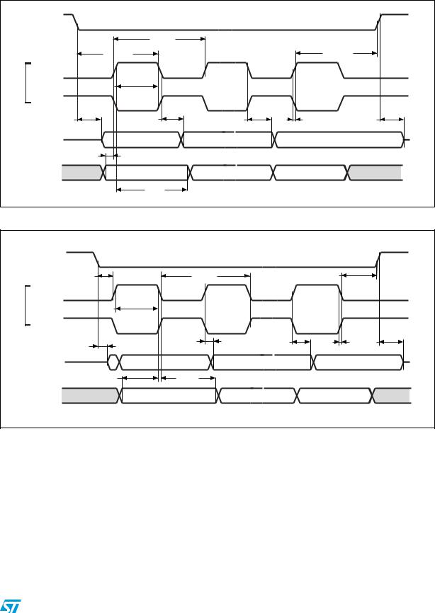
Figure 29. SPI timing diagram - slave mode and CPHA = 0 |
|
|
NSS input |
|
|
|
|
|
|
tc(SCK) |
|
|
|
|
|
tSU(NSS) |
|
th(NSS) |
|
Input |
CPHA= 0 |
|
|
|
|
CPOL=0 |
tw(SCKH) |
|
|
|
|
|
|
|
|
||
SCK |
CPHA= 0 |
tw(SCKL) |
|
|
|
CPOL=1 |
|
|
|
|
|
|
ta(SO) |
tv(SO) |
th(SO) |
tr(SCK) |
tdis(SO) |
|
MISO |
|
|
tf(SCK) |
|
|
MS B O UT |
BI T6 OUT |
LSB OUT |
|
|
|
OUT P UT |
|
|||
|
|
|
|
|
|
|
|
tsu(SI) |
|
|
|
|
MOSI |
M SB IN |
B I T1 IN |
LSB IN |
|
|
I NPUT |
|
|||
|
|
|
|
|
|
|
|
th(SI) |
|
|
ai14134c |
|
|
|
|
|
|
Figure 30. SPI timing diagram - slave mode and CPHA = 1(1) |
|
|
||||
|
NSS input |
|
|
|
|
|
|
|
tSU(NSS) |
tc(SCK) |
|
th(NSS) |
|
Input |
CPHA=1 |
|
|
|
|
|
CPOL=0 |
tw(SCKH) |
|
|
|
|
|
CPHA=1 |
|
|
|
|
||
SCK |
tw(SCKL) |
|
|
|
|
|
CPOL=1 |
|
|
|
|
|
|
|
|
ta(SO) |
tv(SO) |
th(SO) |
tr(SCK) |
tdis(SO) |
|
MISO |
|
|
tf(SCK) |
|
|
|
|
MS B O UT |
BI T6 OUT |
|
LSB OUT |
|
|
OUT P UT |
|
|
|||
|
|
|
|
|
|
|
|
|
tsu(SI) |
th(SI) |
|
|
|
|
MOSI |
|
M SB IN |
B I T1 IN |
LSB IN |
|
|
I NPUT |
|
||||
|
|
|
|
|
|
|
|
|
|
|
|
|
ai14135 |
1. Measurement points are done at CMOS levels: 0.3VDD and 0.7VDD.
Doc ID 16455 Rev 3 |
65/86 |
Electrical characteristics |
STM32F100x4, STM32F100x6, STM32F100x8, STM32F100xB |
|
|
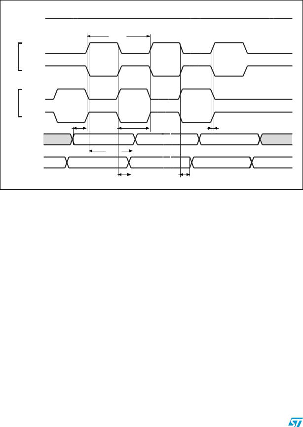
Figure 31. SPI timing diagram - master mode(1)
|
High |
|
|
|
|
NSS input |
|
|
|
|
|
tc(SCK) |
|
|
Input |
CPHA= 0 |
|
|
|
CPOL=0 |
|
|
|
|
|
|
|
|
|
SCK |
CPHA= 0 |
|
|
|
CPOL=1 |
|
|
|
|
Input |
CPHA=1 |
|
|
|
CPOL=0 |
|
|
|
|
|
|
|
|
|
SCK |
CPHA=1 |
|
|
|
CPOL=1 |
|
|
|
|
|
tsu(MI) |
tw(SCKH) |
|
tr(SCK) |
|
tw(SCKL) |
|
tf(SCK) |
|
|
MISO |
MS BIN |
BI T6 IN |
LSB IN |
|
INP UT |
|||
|
|
|
|
|
|
|
th(MI) |
|
|
|
MOSI |
M SB OUT |
B I T1 OUT |
LSB OUT |
|
OUTUT |
|||
|
|
|
|
|
|
|
tv(MO) |
th(MO) |
|
|
|
|
|
ai14136 |
1. Measurement points are done at CMOS levels: 0.3VDD and 0.7VDD.
HDMI consumer electronics control (CEC)
Refer to Section 5.3.12: I/O port characteristics for more details on the input/output alternate function characteristics.
5.3.1612-bit ADC characteristics
Unless otherwise specified, the parameters given in Table 41 are derived from tests performed under the ambient temperature, fPCLK2 frequency and VDDA supply voltage conditions summarized in Table 8.
Note: |
It is recommended to perform a calibration after each power-up. |
66/86 |
Doc ID 16455 Rev 3 |

STM32F100x4, STM32F100x6, STM32F100x8, STM32F100xB |
Electrical characteristics |
||||||||||
|
|
|
|
|
|
|
|
|
|
|
|
Table 41. |
ADC characteristics |
|
|
|
|
|
|
|
|
|
|
|
|
|
|
|
|
|
|
|
|
||
Symbol |
Parameter |
|
Conditions |
Min |
|
Typ |
|
Max |
Unit |
||
|
|
|
|
|
|
|
|
|
|
|
|
VDDA |
Power supply |
|
|
|
2.4 |
|
|
|
3.6 |
V |
|
VREF+ |
Positive reference voltage |
|
|
|
2.4 |
|
|
|
VDDA |
V |
|
I |
|
Current on the VREF input |
|
|
|
|
|
(1) |
|
(1) |
µA |
|
pin |
|
|
|
|
|
160 |
|
220 |
||
VREF |
|
|
|
|
|
|
|
|
|
||
|
|
|
|
|
|
|
|
|
|
|
|
fADC |
ADC clock frequency |
|
|
|
0.6 |
|
|
|
12 |
MHz |
|
fS(2) |
Sampling rate |
|
|
|
0.05 |
|
|
|
1 |
MHz |
|
|
|
|
|
|
|
|
|
|
|
||
|
(2) |
External trigger frequency |
fADC = 12 MHz |
|
|
|
|
823 |
kHz |
||
fTRIG |
|
|
|
|
|
|
|
17 |
1/fADC |
||
|
|
|
|
|
|
|
|
|
|
||
|
(3) |
Conversion voltage range |
|
|
|
0 (VSSA tied to |
|
|
|
VREF+ |
V |
VAIN |
|
|
|
ground) |
|
|
|
||||
|
(2) |
External input impedance |
See Equation 1 and |
|
|
|
|
50 |
k |
||
RAIN |
Table 42 for details |
|
|
|
|
||||||
|
(2) |
Sampling switch resistance |
|
|
|
|
|
|
|
1 |
k |
RADC |
|
|
|
|
|
|
|
||||
|
(2) |
Internal sample and hold |
|
|
|
|
|
|
|
8 |
pF |
CADC |
capacitor |
|
|
|
|
|
|
|
|||
|
(2) |
Calibration time |
fADC = 12 MHz |
|
5.9 |
|
|
µs |
|||
tCAL |
|
|
|
|
83 |
|
|
1/fADC |
|||
|
|
|
|
|
|
|
|
|
|||
t |
(2) |
Injection trigger conversion |
fADC = 12 MHz |
|
|
|
|
0.214 |
µs |
||
lat |
latency |
|
|
|
|
|
|
|
(4) |
1/fADC |
|
|
|
|
|
|
|
|
|
|
|
3 |
|
|
(2) |
Regular trigger conversion |
fADC = 12 MHz |
|
|
|
|
0.143 |
µs |
||
tlatr |
latency |
|
|
|
|
|
|
|
|
|
|
|
|
|
|
|
|
|
(4) |
1/fADC |
|||
|
|
|
|
|
|
|
|
|
|
2 |
|
t |
(2) |
Sampling time |
f |
|
= 12 MHz |
0.125 |
|
|
|
17.1 |
µs |
ADC |
|
|
|
|
|
|
|||||
|
|
|
|
|
|
||||||
|
S |
|
|
|
1.5 |
|
|
|
239.5 |
1/fADC |
|
|
|
|
|
|
|
|
|
|
|||
|
(2) |
Power-up time |
|
|
|
0 |
|
0 |
|
1 |
µs |
tSTAB |
|
|
|
|
|
||||||
|
|
Total conversion time |
fADC = 12 MHz |
1.17 |
|
|
|
21 |
µs |
||
|
(2) |
|
|
|
|
|
|
|
|
|
|
|
|
|
|
|
|
|
|
|
|
||
tCONV |
(including sampling time) |
|
|
|
14 to 252 (tS for sampling +12.5 for |
1/fADC |
|||||
|
|
|
|
|
|
successive approximation) |
|
||||
|
|
|
|
|
|
|
|
|
|
|
|
1.Based on characterization results, not tested in production.
2.Guaranteed by design, not tested in production.
3.In devices delivered in LQFP packages, VREF+ is internally connected to VDDA and VREF- is internally connected to VSSA. Devices that come in the TFBGA64 package have a VREF+ pin but no VREF- pin (VREF- is internally connected to VSSA), see Table 4: STM32F100xx pin definitions and Figure 6.
4.For external triggers, a delay of 1/fPCLK2 must be added to the latency specified in Table 41.
Equation 1: RAIN max formula: |
|||||
RAIN |
|
|
TS |
– RADC |
|
----------- |
-----C----- |
----------- |
-----ln--------2---N----+----2--- |
||
f |
ADC |
ADC |
|
||
|
|
|
|
||
Doc ID 16455 Rev 3 |
67/86 |

Electrical characteristics |
STM32F100x4, STM32F100x6, STM32F100x8, STM32F100xB |
|
|
The above formula (Equation 1) is used to determine the maximum external impedance allowed for an error below 1/4 of LSB. Here N = 12 (from 12-bit resolution).
Table 42. R |
AIN |
max for f |
ADC |
= 12 MHz(1) |
|
|
|
|
|
|
|||
Ts (cycles) |
|
|
tS (µs) |
RAIN max (k ) |
||
|
|
|
|
|
|
|
1.5 |
|
|
|
0.125 |
0.4 |
|
|
|
|
|
|
|
|
7.5 |
|
|
|
0.625 |
5.9 |
|
|
|
|
|
|
|
|
13.5 |
|
|
|
1.125 |
11.4 |
|
|
|
|
|
|
|
|
28.5 |
|
|
|
2.375 |
25.2 |
|
|
|
|
|
|
|
|
41.5 |
|
|
|
3.45 |
37.2 |
|
|
|
|
|
|
|
|
55.5 |
|
|
|
4.625 |
50 |
|
|
|
|
|
|
|
|
71.5 |
|
|
|
5.96 |
NA |
|
|
|
|
|
|
|
|
239.5 |
|
|
|
20 |
NA |
|
|
|
|
|
|
|
|
1. Guaranteed by design, not tested in production.
Table 43. |
ADC accuracy - limited test conditions(1)(2) |
|
|
|
||
Symbol |
Parameter |
Test conditions |
Typ |
Max |
Unit |
|
|
|
|
|
|
|
|
ET |
Total unadjusted error |
fPCLK2 = 24 MHz, |
±1.5 |
±2.5 |
|
|
|
|
fADC = 12 MHz, RAIN < 10 k , |
|
|
|
|
EO |
Offset error |
±1 |
±2 |
|
||
VDDA = 3 V to 3.6 V |
|
|||||
|
|
|
|
|
||
EG |
Gain error |
±0.5 |
±1.5 |
LSB |
||
VREF+ = VDDA |
||||||
|
|
|
|
|||
ED |
Differential linearity error |
TA = 25 °C |
±1.5 |
±2 |
|
|
|
|
Measurements made after |
|
|
|
|
EL |
Integral linearity error |
±1.5 |
±2 |
|
||
ADC calibration |
|
|||||
|
|
|
|
|
||
|
|
|
|
|
|
|
1.ADC DC accuracy values are measured after internal calibration.
2.Based on characterization, not tested in production.
Table 44. ADC accuracy(1) (2) (3)
Symbol |
Parameter |
Test conditions |
Typ |
Max |
Unit |
|
|
|
|
|
|
|
|
ET |
Total unadjusted error |
fPCLK2 = 24 MHz, |
±2 |
±5 |
|
|
|
|
|
|
|
||
EO |
Offset error |
fADC = 12 MHz, RAIN < 10 k , |
±1.5 |
±2.5 |
|
|
|
|
VDDA = 2.4 V to 3.6 V |
|
|
|
|
EG |
Gain error |
±1.5 |
±3 |
LSB |
||
TA = Full operating range |
||||||
|
|
|
|
|
||
ED |
Differential linearity error |
±1.5 |
±2.5 |
|
||
Measurements made after |
|
|||||
|
|
ADC calibration |
|
|
|
|
EL |
Integral linearity error |
±1.5 |
±4.5 |
|
||
|
|
|||||
|
|
|
|
|
|
1.ADC DC accuracy values are measured after internal calibration.
2.Better performance could be achieved in restricted VDD, frequency, VREF and temperature ranges.
3.Based on characterization, not tested in production.
Note: ADC accuracy vs. negative injection current: Injecting a negative current on any of the standard (non-robust) analog input pins should be avoided as this significantly reduces the accuracy of the conversion being performed on another analog input. It is recommended to
68/86 |
Doc ID 16455 Rev 3 |
STM32F100x4, STM32F100x6, STM32F100x8, STM32F100xB |
Electrical characteristics |
|
|
add a Schottky diode (pin to ground) to standard analog pins which may potentially inject negative currents.
Any positive injection current within the limits specified for IINJ(PIN) and IINJ(PIN) in Section 5.3.12 does not affect the ADC accuracy.
Figure 32. ADC accuracy characteristics |
|
||||||||
|
[1LSB |
|
V |
|
V |
DDA depending on package)] |
|
||
|
IDEAL |
= REF+ (or |
|
|
|||||
|
|
4096 |
4096 |
|
|
|
|||
|
|
|
|
|
|
||||
4095 |
|
|
|
|
|
|
|
EG |
(1) Example of an actual transfer curve |
|
|
|
|
|
|
|
|
||
|
|
|
|
|
|
|
|
(2) The ideal transfer curve |
|
4094 |
|
|
|
|
|
|
|
|
|
|
|
|
|
|
|
|
|
(3) End point correlation line |
|
4093 |
|
|
|
|
|
|
|
|
|
|
|
|
|
|
|
|
|
(2) |
ET=Total Unadjusted Error: maximum deviation |
|
|
|
|
|
|
ET |
|
|
|
7 |
|
|
|
|
|
|
(3) |
between the actual and the ideal transfer curves. |
|
|
|
|
|
|
|
|
EO=Offset Error: deviation between the first actual |
||
|
|
|
|
|
|
|
(1) |
||
6 |
|
|
|
|
|
|
|
transition and the first ideal one. |
|
|
|
|
|
|
|
|
|
EG=Gain Error: deviation between the last ideal |
|
|
|
|
|
|
|
|
|
|
|
5 |
EO |
|
|
|
|
EL |
|
transition and the last actual one. |
|
4 |
|
|
|
|
|
ED=Differential Linearity Error: maximum deviation |
|||
|
|
|
|
|
|
|
|
between actual steps and the ideal one. |
|
3 |
|
|
|
|
|
|
|
ED |
EL=Integral Linearity Error: maximum deviation |
|
|
|
|
|
|
|
|
between any actual transition and the end point |
|
2 |
|
|
|
|
|
|
|
|
correlation line. |
1 |
|
|
|
|
1 LSBIDEAL |
|
|
||
0 |
1 |
2 |
3 |
4 |
5 |
6 |
7 |
4093 4094 4095 4096 |
|
|
|
||||||||
VSSA |
|
|
|
|
|
|
VDDA |
ai14395b |
|
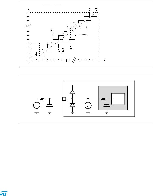
Figure 33. Typical connection diagram using the ADC
|
VDD |
STM32F10xxx |
|||
|
|
|
|
|
|
|
|
|
VT |
Sample and hold ADC |
|
|
|
|
converter |
||
|
|
|
|||
RAIN(1) |
|
0.6 V |
RADC(1) |
AINx |
|
||
|
|
|
12-bit |
|
|
|
converter |
VAIN |
|
VT |
|
|
0.6 V |
CADC(1) |
|
Cparasitic |
|
||
|
|
|
IL±1 µA |
ai14139d
1.Refer to Table 41 for the values of RAIN, RADC and CADC.
2.Cparasitic represents the capacitance of the PCB (dependent on soldering and PCB layout quality) plus the pad capacitance (roughly 7 pF). A high Cparasitic value will downgrade conversion accuracy. To remedy this, fADC should be reduced.
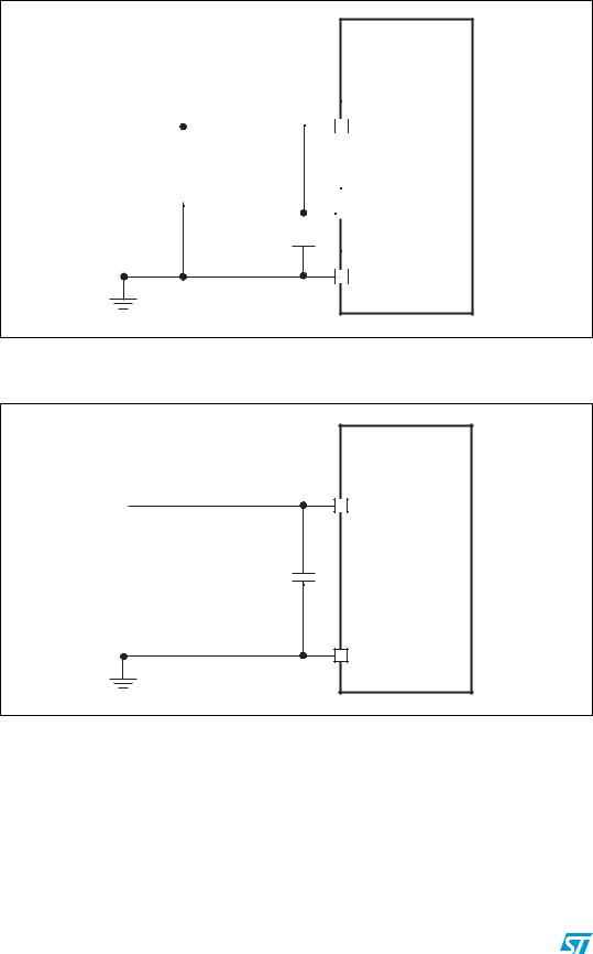
General PCB design guidelines
Power supply decoupling should be performed as shown in Figure 34 or Figure 35,
depending on whether VREF+ is connected to VDDA or not. The 10 nF capacitors should be ceramic (good quality). They should be placed them as close as possible to the chip.
Doc ID 16455 Rev 3 |
69/86 |
Electrical characteristics |
STM32F100x4, STM32F100x6, STM32F100x8, STM32F100xB |
|
|
Figure 34. Power supply and reference decoupling (VREF+ not connected to VDDA)
STM32F10xxx
V REF+
|
|
|
|
|
|
|
|
|
|
|
|
1 µF // 10 nF |
|
|
|
|
|
|
|
|
|
V DDA |
|
|
|
|
|
|
|
|
|
|
|||
|
|
|
|
|
|
|
|
|
|||
|
|
|
|
|
|
|
|
|
|||
|
|
|
|
|
|
|
|
|
|
|
|
|
|
|
|
|
|
|
|
|
|
|
|
1 µF // 10 nF
V SSA/V REF-
ai14380b
1.VREF+ is available on 100-pin packages and on TFBGA64 packages. VREF- is available on 100-pin packages only.
Figure 35. Power supply and reference decoupling (VREF+ connected to VDDA)
STM32F10xxx
VREF+/VDDA
1 µF // 10 nF
VREF–/VSSA
ai14381b
1. VREF+ and VREF- inputs are available only on 100-pin packages.
70/86 |
Doc ID 16455 Rev 3 |