

Allen and Holberg - CMOS Analog Circuit Design
.pdfAllen and Holberg - CMOS Analog Circuit Design |
Page V.4-10 |
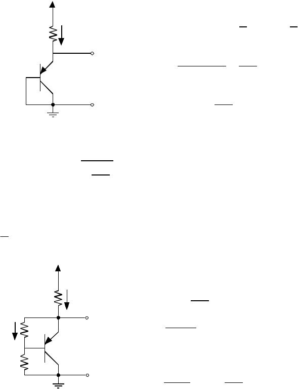
Output Impedance of the Wilson Current Source
|
|
|
|
|
iout |
|
|
|
+ |
|
+ |
|
|
|
|
|
|
|
iin=0 |
|
v3 rds3 |
gm3(v1-v2) |
gmbs3v2 |
|
|
|
- |
||
|
|
+ |
|
+ |
vout |
|
|
|
|
||
gm1v2 |
rds1 |
v1 |
gm2v2 |
rds2 v2 |
|
|
|
- |
- |
- |
|
|
|
|
|
vout = rds3[iout - gm3v1 + gm3v2 + gmbs3v2] + v2
vout = rds3iout - gm3rds3(-gm1rds1v2) + gm3rds3v2 + gmbs3rds3v2 + v2
v |
|
= i |
|
rds2 |
|
2 |
|
|
|
||
|
|
out 1 + gm2 rd s 2 |
|||
vout = ioutrds3 + [gm3rds3 + gmbs3rds3 + gm1rds1gm3rds3]v2 + v2
r |
|
= r |
|
+ r |
1 + gm3rds3 + gmbs3rds3 + gm1rds1gm3rds3 |
||
out |
ds3 |
|
1+gm2rds2 |
|
|||
|
|
|
ds2 |
|
|||
rout ≈ |
rds2gm1rds1gm3rds3 |
≈ rd s 1 |
× (gm 3 rd s 3 ) if gm 1 |
= gm 2 |
|
gm2rds2 |
|||||
|
|
|
|


 M1
M1 M2
M2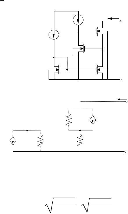
Allen and Holberg - CMOS Analog Circuit Design |
Page V.4-12 |
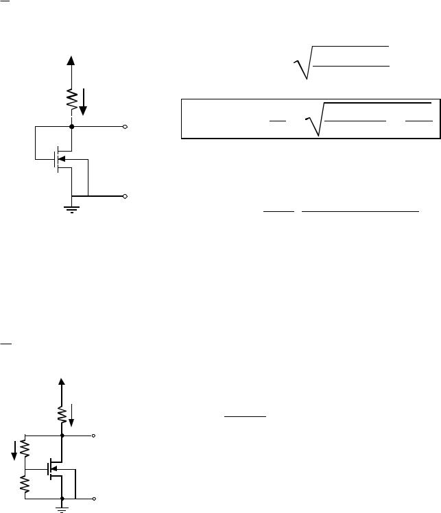
Regulated Cascode Current Mirror
VDD |
|
|
iOUT |
|
|
|
|
|
IB |
M4 |
+ |
|
|
||
|
|
|
|
IIN |
|
|
|
|
M3 |
|
|
|
+ |
|
vOUT |
M1 |
vGS4 |
M2 |
|
- |
|
-
VSS
Small Signal Equivalent Model (gmbs effects ignored) -
|
|
|
iout |
|
|
|
+ |
|
rds4 |
|
gm4vgs4 |
v4 |
|
|
|
|
|
|
|
|
|
+ |
vout |
rds3 |
rds2 |
v3 |
|
gm3 v3 |
|
- |
- |
|
|
vout = (iout - gm4vgs4)rds4 + ioutrds2 vgs4 = v4 - v3
v3 = ioutrds2
v4 = -gm3v3rds3
vout = ioutrds4 - gm4(-gm3ioutrds2rds3 - ioutrds2)rds4 + ioutrds2 rout = rds4 + gm4gm3 rds2rds3rds4 + rds2 + gm4rds2rds4
vOUT(min) = |
2IB |
|
2Iout |
K'(W/L)4 |
+ |
+ VT4 |
|
|
|
K'(W/L)3 |

Allen and Holberg - CMOS Analog Circuit Design |
Page V.5-1 |
V.5 - REFERENCE CIRCUITS
Introduction
What is a Reference Circuit?
A reference circuit is an independent voltage or current source which has a high degree of precision and stability.
Requirements for a Reference Circuit
1.) Output voltage/current should be independent of power supply.
2.) Output voltage/current should be independent of temperature.
3.) Output voltage/current should be independent of processing variations.
V-I Characteristics of an Ideal Reference
i
Voltage Reference
Iref
Current Reference
 v
v
Vref

Allen and Holberg - CMOS Analog Circuit Design |
Page V.5-2 |
Concept of Sensitivity
Definition
Sensitivity is a measure of dependence of Vref (Iref) upon a parameter or
variable x which influences Vref (Iref).
Vref |
|
∂Vref |
|
x ∂Vref |
|
= |
Vref |
||||
S |
∂x |
= |
|
|
|
|
|
Vref |
∂x |
||
x |
|
x |
|
|
|
|
|
|
|
||
where
x = VDD or temperature
Application of Sensitivity
∂Vref |
Vref |
|
|
|
∂x |
||
Vref |
= |
S |
x |
|
|
x |
|
For example, if the sensitivity is 1, then a 10% change in x will cause a 10% change in Vref.
Vref
Ideally, S → 0
x

Allen and Holberg - CMOS Analog Circuit Design |
Page V.5-3 |
V.5-1 - SIMPLE REFERENCES
Objective is to minimize,
Vref |
|
∂ V r e f |
|
|
Vref |
||
S |
= |
||
∂ V D D |
|||
VDD |
|
||
|
VDD |
||
|
|
Types of references include,
1.Voltage dividers - passive and active.
2.MOS diode reference.
3.PN junction diode reference.
4.Gate-source threshold referenced circuit.
5.Base-emitter referenced circuit.
Allen and Holberg - CMOS Analog Circuit Design |
Page V.5-4 |
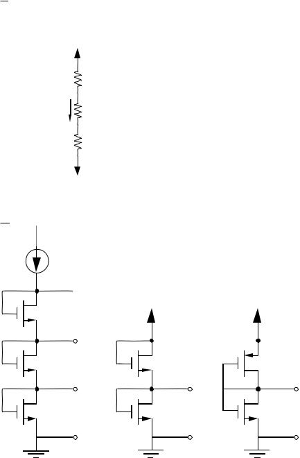
Passive Divider
Accuracy is approximately equivalent to 6 bits (1/64).
VDD
RA
 V1
V1
I RB
 V2
V2
RC
VSS
Active Dividers
I
 V3
V3
M3 |
|
VDD |
VDD |
|
|
|
|
|
V2 |
|
|
M2 |
|
M2 |
M2 |
|
V1 |
+ |
+ |
|
|
||
M1 |
|
M1 V |
M1 V |
|
|
ref |
ref |
|
|
- |
- |
Allen and Holberg - CMOS Analog Circuit Design Page V.5-6
Gate-Source Referenced Circuits
(MOS equivalent of the pn junction referenced circuit)
VDD |
|
|
|
|
2(VDD-VREF) |
|
|
|
VREF = VGS = VT + |
|
|
||
|
|
|
βR |
|
||
R |
I |
|
1 |
|
2(VDD-VT) |
1 |
|
|
|
|
|||
|
+ |
V R E F = VT − βR |
+ |
βR |
+ β2R2 |
|
|
VREF |
|
|
|
|
|
|
- |
Sensitivity: |
|
|
|
|
|
VREF |
|
|
|
|
|
|
|
VDD |
1 |
|
||
|
|
S |
||||
|
|
= VREF 1 + βR(VREF - VT ) |
||||
|
|
VDD |
|
|
|
|
If VDD = 10V, W/L = 10, R = 100kΩ and using the results of Table 3.1-2 gives
VREF
VREF = 1.97V.and S = 0.29.
VDD
Modifying the Value of VREF
VDD
R |
I |
|
R1 +R2 |
|
||
VREF |
≈ |
R2 |
VGS |
|||
|
|
|||||
|
|
|
|
|
||
IR1 |
+ |
|
R1 |
||
|
||
|
VREF |
|
|
R2 |
|
|
- |