

Allen and Holberg - CMOS Analog Circuit Design
.pdfAllen and Holberg - CMOS Analog Circuit Design |
Page V.3-4 |
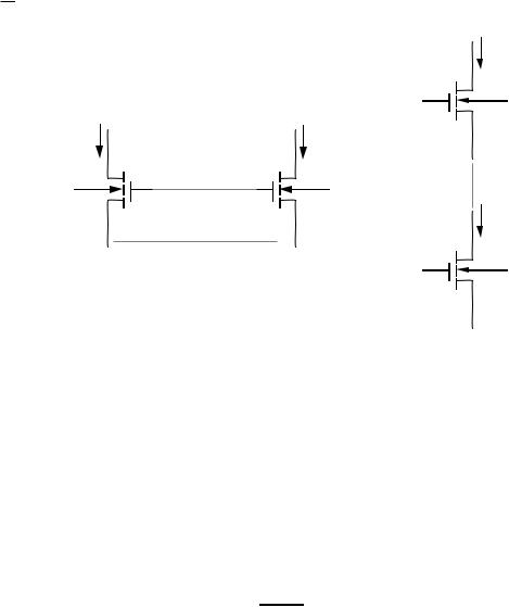
CASCODE CURRENT SINK
MOS
Circuit |
Small-Signal Model |
|
||
IREF |
iOUT |
|
|
iout |
+ |
|
|
||
M4 |
M2 |
|
|
+ |
|
|
|
|
|
|
vOUT |
gm2vgs2 |
|
r ds2 |
|
gmbs2vbs2 |
|
|
|
M3 M1 |
- |
|
+ |
vout |
|
|
|
||
|
|
r ds1 |
|
|
|
|
vS2 |
|
|
|
|
gm1vgs1 |
- |
- |
vout
vout
rout
Note : vMIN
=[iout - (gm2vgs2 + gmbs2vbs2)]rds2 + ioutrds1
=iout[rds2 + gm2rds2r(1 + η2) + rds1]
=rds2 + r[1 + gm2rds2(1 + η2)] rds1gm2rds2(1 + η2)
= VT + 2VON 0.75 + 1.5 = 2.25 (assuming VON ≈ VT)
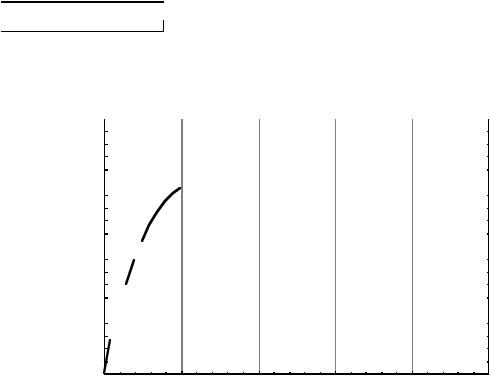
NMOS Cascode-
1mA |
|
|
|
|
|
Slope = 1/Ro |
|
|
||
|
|
|
|
|
|
|
||||
|
|
|
|
|
|
|
|
|||
0.75mA |
|
|
|
|
|
|
|
|
iO |
|
|
|
|
|
|
|
+ |
|
+ |
||
iO 0.5mA |
|
|
|
|
|
|
|
|
||
|
|
|
|
|
|
|
|
|
||
|
|
|
|
|
|
vGS2 |
|
|
||
|
|
|
|
|
|
|
- |
|
vO |
|
|
|
|
|
|
|
|
|
|
|
|
0.25mA |
|
|
|
|
|
|
+ |
|
|
|
|
|
|
|
|
|
vGS1 |
|
|
||
|
|
|
|
|
|
|
- |
|
||
|
|
|
|
|
VMIN |
- |
|
|
||
0mA |
|
|
|
|
|
|
|
|
||
|
|
|
|
|
|
|
|
|||
|
2V |
4V |
|
6V |
|
8V |
10V |
|||
0V |
|
|
||||||||
|
|
|
|
vO |
|
|
|
|
|
|

 S
S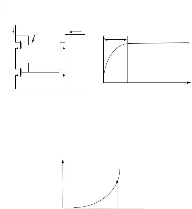
 v
v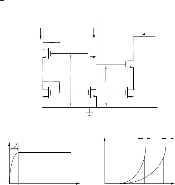


Allen and Holberg - CMOS Analog Circuit Design |
Page V.3-11 |
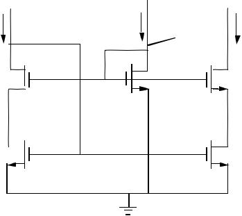
CMOS REGULATED CASCODE CURRENT SOURCE
Circuit Diagram
VDD |
VDD |
|
iOUT |
iD3 |
|
|
|
|
|
||
|
IB2 |
RB2 |
|
|
|
|
|
M3 |
+ |
|
vGS3 |
|
|
|
|
|
|
IB1 |
|
|
|
|
|
|
M4 |
|
vOUT |
Iout |
|
|
|
|
|
||
M1 |
|
M2 |
|
|
|
|
|
|
|
|
|
|
|
|
- |
VDS3(min) |
vDS3 |
|
|
|
|
VDS3(sat) |
Principle of operation:
As vOUT decreases, M3 will enter the non-saturation region and iOUT will begin to decrease. However, this causes a decrease in the gate-
source voltage of M4 which causes an increase in the gate voltage of M3. The minimum value of vOUT is determined by the gate-source voltage of
M4 and Vdsat of M3. Assume that all devices are in saturation.
vOUT(min) = |
2IB2 |
|
2Iout |
K'(W/L)4 |
+ |
+ VT4 |
|
|
|
K'(W/L)3 |
Allen and Holberg - CMOS Analog Circuit Design |
Page V.3-12 |
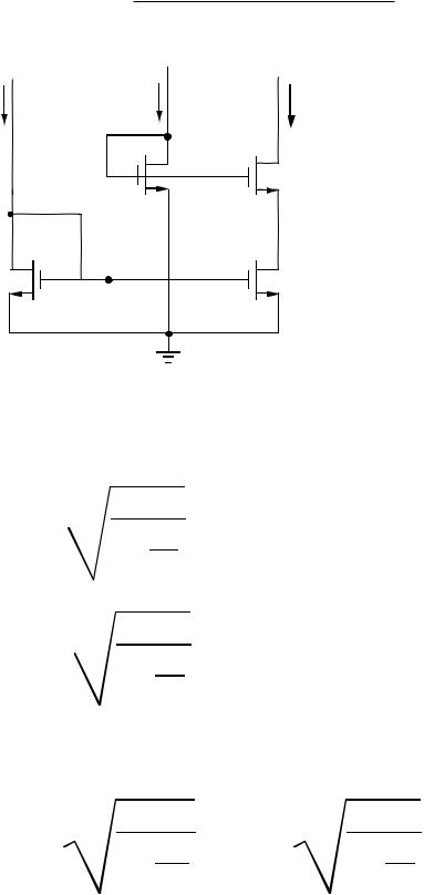
CMOS REGULATED CASCODE CURRENT SOURCE - CONT.
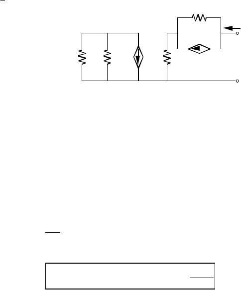
Small Signal Model
|
|
|
r ds3 |
|
|
+ |
vgs3 |
- |
|
iout |
|
gm3vgs3 |
+ |
||||
|
+ |
||||
|
|
|
|||
RB2 r ds4 |
vgs4 |
|
r ds2 |
vout |
|
gm4vgs4 |
|
- |
|
|
|
-
(Ignore bulk effects)
iout = gm3vgs3 + gds3(vout - vgs4)
vgs4 = ioutrds2
vgs3 = vg3 - vs3 = -gm4(rds4||RB2)vgs4 - vgs4
=-rds2[1 + gm4(rds4||RB2)]iout
iout = -gm3rds2[1 + gm4(rds4||RB2)]iout + gds3vout - gds3rds2iout
Solving for vout,
vout = rds3[1 + gm3rds2 + gds3rds2 + gm3rds2gm4(rds4||RB2)]iout
rout = |
vout |
+ gds3rds2 + gm3rds2gm4(rds4||RB2)] |
||
= rds3[1 + gm3rds2 |
||||
|
iout |
|
|
|
|
|
g |
m |
2r3 |
|
rout = rds3gm3rds2gm4(rds4||RB2) = |
|
||
|
2 |
|||
Example
K'N = 25µA/V2, λ = 0.01, IB1 = IB2 = 100µA, all transistors with minimum geometry (W = 3µm, L=3µm), and RB2 = rds, we get
rds = 1MΩ and gm = 70.7µmho
rout≈ (1MΩ)(70.7µmho)((1MΩ)(70.7µmho)(1MΩ||1MΩ)= 2.5GΩ!!!
