

Allen and Holberg - CMOS Analog Circuit Design
.pdfAllen and Holberg - CMOS Analog Circuit Design |
II.8-7 |
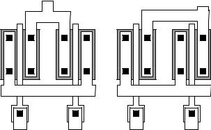
Transistor Layout
Metal |
|
|
FOX |
FOX |
|
Active area |
Polysilicon |
|
drain/source |
||
gate |
||
|
||
Contact |
L |
|
Cut |
|
|
|
W |
|
Active area |
|
|
drain/source |
|
Metal 1
Figure 2.6-3 Example layout of an MOS transistor showing top view and side view at the cut line indicated.
Allen and Holberg - CMOS Analog Circuit Design |
II.8-8 |
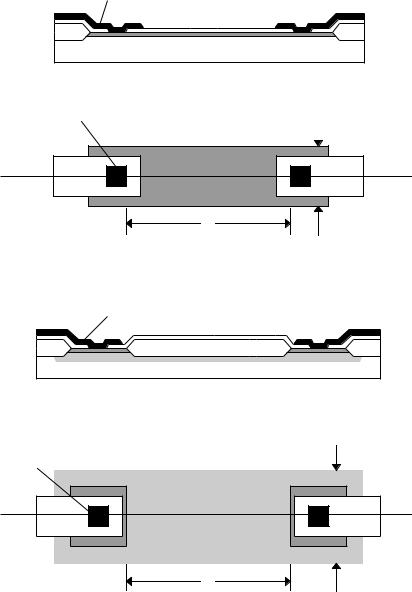
SYMMETRIC VERSUS PHOTOLITHOGRAPHIC INVARIANT
(a) |
(b) |
Figure 2.6-4 Example layout of MOS transistors using (a) mirror symmetry, and
(b) photolithographic invariance.
PLI IS BETTER
Allen and Holberg - CMOS Analog Circuit Design |
II.8-9 |
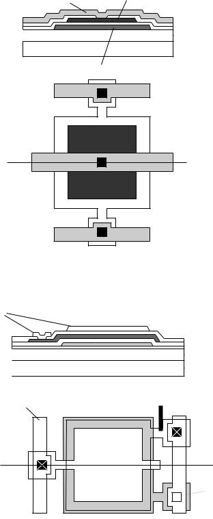
Resistor Layout
Metal
FOX |
FOX |
|
Substrate |
Active area (diffusion)
Contact |
Active area or Polysilicon |
W |
|
|
|
|
|
Cut
L
Metal 1
(a) Diffusion or polysilicon resistor
Metal
FOX |
FOX |
FOX |
Substrate |
|
|
Active area (diffusion) |
Well diffusion |
|
Active area |
W |
|
Well diffusion |
||
|
Contact
Cut
Metal 1
L
(b) Well resistor
Figure 2.6-5 Example layout of (a) diffusion or polysilicon resistor and (b) Well resistor along with their respective side views at the cut line indicated.
Allen and Holberg - CMOS Analog Circuit Design |
II.8-10 |
Capacitor Layout
Metal |
Polysilicon 2 |
|
|
FOX |
|
Substrate |
|
|
Polysilicon gate |
|
Polysilicon gate |
Polysilicon 2 |
|
Cut |
|
|
Metal 1 |
(a)
Metal 3 |
Metal 2 |
Metal 1 |
FOX
Substrate
Metal 3 |
Metal 2 |
Metal 1 |
|
Metal 3 |
Via 2
Via 2
Metal 2
Cut
Via 1
Metal 1
Allen and Holberg - CMOS Analog Circuit Design |
Page III.0-1 |
III. CMOS MODELS
Contents
III.1 |
Simple MOS large-signal model |
|
Strong inversion |
|
Weak inversion |
III.2 |
Capacitance model |
III.3 |
Small-signal MOS model |
III.4 |
SPICE Level-3 model |
Perspective |
|
|
|
|
Chapter 10 |
Chapter 11 |
|||
D/A and A/D |
||||
Analog Systems |
||||
Converters |
||||
|
|
|||
SYSTEMS |
|
|
|
|
Chapter 7 |
|
Chapter 8 |
Chapter 9 |
|
CMOS |
Simple CMOS OP |
High Performance |
||
Comparators |
|
AMPS |
OTA's |
|
COMPLEX |
|
|
|
|
CIRCUITS |
|
|
|
|
Chapter 5 |
|
Chapter 6 |
||
CMOS |
|
CMOS Amplifiers |
||
Subcircuits |
|
|
||
SIMPLE |
|
|
|
|
Chapter 2 |
|
Chapter 3 |
Chapter 4 Device |
|
CMOS |
CMOS Device |
|||
Characterization |
||||
Technology |
|
Modeling |
||
|
|
|||
DEVICES |
|
|
|
|

Allen and Holberg - CMOS Analog Circuit Design |
Page III.1-1 |
III.1 - MODELING OF CMOS ANALOG CIRCUITS
Objective
1.Hand calculations and design of analog CMOS circuits.
2.Efficiently and accurately simulate analog CMOS circuits.
Large Signal Model
The large signal model is nonlinear and is used to solve for the dc values of the device currents given the device voltages.
The large signal models for SPICE:
Basic drain current models -
1.Level 1 - Shichman-Hodges (VT, K', γ, λ, φ, and NSUB)
2.Level 2 - Geometry-based analytical model. Takes into account second-order effects (varying channel charge, short-channel, weak inversion, varying surface mobility, etc.)
3.Level 3 - Semi-empirical short-channel model
4.Level 4 - BSIM model. Based on automatically generated parameters from a process characterization. Good weak-strong inversion transition.
Basic model auxilliary parameters include capacitance [Meyer and Ward-Dutton (charge-conservative)], bulk resistances, depletion regions, etc..
Small Signal Model
Based on the linearization of any of the above large signal models.
Simulator Software
SPICE2 - Generic SPICE available from UC Berkeley (FORTRAN)
SPICE3 - Generic SPICE available from UC Berkeley (C)
*SPICE*- Every other SPICE simulator!

Allen and Holberg - CMOS Analog Circuit Design |
Page III.1-2 |
Transconductance Characteristics of NMOS when VDS = 0.1V
vGS ≤ VT:
|
+ |
|
iD |
+ |
iD |
|
vGS |
|
|
||
Source |
= VT - |
|
|
VDS |
|
Gate |
Drain |
- =0.1V |
|
||
and |
|
|
|
bulk
|
0 |
p substrate (bulk) |
0 VT 2VT 3VT vGS |
|
vGS = 2VT:
|
|
|
+ |
|
iD |
+ |
|||||
|
|
|
|
vGS |
|
||||||
Source |
|
= 2VT - |
|
|
|
|
|
|
VDS |
||
|
Gate |
Drain |
- =0.1V |
||||||||
and |
|
|
|
||||||||
|
bulk |
|
|
|
|
|
|
|
|
|
|
|
|
|
|
|
|
|
|
|
|
||
|
|
|
|
|
|
|
|
|
|||
|
|
|
|
|
|
|
|
|
|
|
|
|
|
|
|
|
|
|
|
|
|
|
|
|
|
|
|
|
|
|
|
|
|
|
|
|
|
|
|
|
|
|
|
|
|
|
|
|
|
|
|
|
|
|
|
|
|
|
|
p substrate (bulk)
vGS = 3VT:
|
|
|
|
+ |
|
iD |
+ |
|||||
|
|
|
|
|
vGS |
|
||||||
Source |
|
= 3VT |
|
|
|
|
|
|
VDS |
|||
and |
- |
Gate |
Drain |
- =0.1V |
||||||||
|
|
|
||||||||||
|
bulk |
|
|
|
|
|
|
|
|
|
||
|
|
|
|
|
|
|
|
|
|
|||
|
|
|
|
|
|
|
|
|
||||
|
|
|
|
|
|
|
|
|
|
|
|
|
|
|
|
|
|
|
|
|
|
|
|
|
|
|
|
|
|
|
|
|
|
|
|
|
|
|
|
|
|
|
|
|
|
|
|
|
|
|
|
|
|
|
|
|
|
|
|
|
|
|
|
|
p substrate (bulk)
iD
0
0 VT 2VT 3VT vGS
iD
0
0 V |
2VT |
3VT |
vGS |
T |
|
|

Allen and Holberg - CMOS Analog Circuit Design |
Page III.1-3 |
Output Characteristics of NMOS for VGS = 2VT
vDS = 0V:
|
VGS + |
|
iD |
+ vDS iD |
|
Source |
= 2VT - |
Gate |
|
- |
= 0V |
and |
|
Drain |
|
||
|
|
|
|||
bulk
0
p substrate (bulk)
0 0.5VT VT vDS
vDS = 0.5VT:
|
|
|
VGS + |
|
|
iD |
||
Source |
= 2VT - |
Gate |
|
|
|
|
||
and |
|
Drain |
||||||
bulk |
|
|
|
|
|
|
||
|
|
|
|
|
|
|||
|
|
|
|
|
|
|
|
|
|
|
|
|
|
|
|
|
|
|
|
|
|
|
|
|
|
|
|
|
|
|
|
|
|
|
|
|
|
|
|
|
|
|
|
|
p substrate (bulk)
vDS = VT:
|
|
|
|
|
|
VGS + |
|
|
|
iD |
|||
Source |
= 2VT - |
Gate |
|
Drain |
|||||||||
and |
|
|
|
||||||||||
|
bulk |
|
|
|
|
|
|
|
|
|
|||
|
|
|
|
|
|
|
|
|
|
||||
|
|
|
|
|
|
|
|
|
|
|
|
|
|
|
|
|
|
|
|
|
|
|
|
|
|
|
|
|
|
|
|
|
|
|
|
|
|
|
|
|
|
|
|
|
|
|
|
|
|
|
|
|
|
|
|
x
p substrate (bulk)
+ vDS = iD
- 0.5VT
0
0 0.5VT VT vDS
+ |
iD |
v DS |
|
- =VT |
|
0 0.5V T VT vDS

Allen and Holberg - CMOS Analog Circuit Design |
Page III.1-4 |
Output Characteristics of NMOS when vDS = 4VT
vGS = VT:
|
vGS = + |
|
iD |
+ vDS = iD |
|
|
|
Source |
VT - |
Gate |
Drain |
- 4VT |
|
|
|
and |
|
|
|
|
|
||
bulk |
|
|
|
|
|
|
|
|
|
|
|
vDS(sat) |
|
|
|
|
|
|
|
0 |
|
|
4V vDS |
p substrate (bulk) |
|
|
0 V |
2V |
3V |
||
|
|
|
|
T |
T |
T |
T |
vGS = 2VT:
|
vGS = |
+ |
|
iD |
Source |
|
|
||
2VT |
- |
Gate |
Drain |
|
and |
|
|
||
bulk |
|
|
|
|
p substrate (bulk)
vGS = 3VT:
|
vGS = + |
|
iD |
|
Source |
3VT |
- |
Gate |
|
and |
|
Drain |
||
|
|
|||
bulk
p substrate (bulk)
 + vDS = iD
  - 4VT
- 4VT
vDS(sat)
0
0 VT 2VT 3VT 4VT vDS
 + vDS = iD
  - 4VT
- 4VT
vDS(sat)
0
0 VT 2VT 3VT 4VT vDS
Allen and Holberg - CMOS Analog Circuit Design |
Page III.1-5 |
Output Characteristics of an n-channel MOSFET
2.0Output Characteristics of a n-channel MOSFET
.MODEL MN1K100 NMOS VTO=1 KP=200U LAMBDA=0.01
|
.DC VDS 0 10 0.5 VGS 1 5 1 |
VGS=5V |
|
MOSFET1 2 1 0 0 MN1K100 |
|
|
|
|
|
.PRINT DC ID(MOSFET1) |
|
1.5 |
VGS 1 0 |
|
VDS 2 0 |
|
|
|
.PROBE |
|
|
.END |
|
iD (mA) |
|
|
1.0 |
|
VGS=4V |
0.5 |
|
|
|
VGS=3V |
|
|
|
|
|
|
VGS=2V |
|
|
0 |
|
|
|
VGS=1V |
|
|
0 |
2 |
4 |
6 |
|
8 |
10 |
|
|
|
vDS (V) |
|
|
|
Transconductance Characteristics of an n-channel MOSFET |
|
|||||
2.0 |
Transconductance Characteristics of a n-channel MOSFET |
|
VDS=8V |
|
||
|
|
|
||||
|
.MODEL MN1K100 NMOS VTO=1 KP=200U LAMBDA=0.01 |
VDS=6V |
|
|||
|
.DC VGS 0 5 0.5 VDS 2 8 2 |
|
|
|
|
|
|
|
|
|
|
|
|
|
MOSFET1 2 1 0 0 MN1K100 |
|
|
|
VDS=4V |
|
1.5 |
.PRINT DC ID(MOSFET1) |
|
|
|
|
|
|
|
|
|
|
||
|
VGS 1 0 |
|
|
|
|
|
|
VDS 2 0 |
|
|
|
|
|
iD (mA) |
.PROBE |
|
|
|
|
|
.END |
|
|
|
|
VDS=2V |
|
|
|
|
|
|
||
|
|
|
|
|
|
|
1.0
0.5
0
0 |
1 |
2 |
3 |
4 |
5 |
vGS(V)