

Allen and Holberg - CMOS Analog Circuit Design
.pdf V
V M1
M1 Undesired operating point
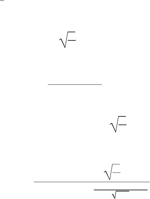
Allen and Holberg - CMOS Analog Circuit Design |
Page V.5-8 |
Bootstrapped Current Sink/Source - Continued
An examination of the second-order effects of this circuitThe relationship between M1 and R can be expressed as,
I2R = VT1 |
+ |
2I1 |
|
β1 |
|||
|
|
Instead of assuming that I1 = I2 because of the current mirror, M3-M4, let us consider the effects of the channel modulation which gives
|
1 + λPV G S 4 |
|
I2 = I1 1 + λP(VD D - VDS1) |
||
Solving for I1 from the above two expressions gives
I1R(1 + λPVGS4) = [1 + λP(VDD-VDS1)] |
2I1 |
|
β1 |
||
|
Differentiating with respect to VDD and assuming the VDS1 and VGS4 are constant gives (IOUT = I1),
|
|
|
|
|
|
|
|
2I |
|
|
|
|
IOUT |
|
20V |
|
λ |
V |
|
+ |
|
|
1 |
|
|
|
DD |
T1 |
β |
|
|
|
|
|||||
|
|
|
|
P |
|
1 |
|
|
||||
S |
= |
|
|
|
|
|
|
|
|
|
||
|
|
|
|
1 + |
λP(VD D - VDS1 ) |
|||||||
VDD |
|
|
|
|
||||||||
|
IOUT R(1 + λPV GS4 ) - |
|
2β1I1 |
|
||||||||
|
|
|
|
|
|
|
|
|
||||
Allen and Holberg - CMOS Analog Circuit Design |
Page V.5-9 |
Bootstrapped Current Sink/Source - Continued
Assume that VDD=5V, KN' = 23.6 µA/V2, VTN=0.79V, γN=0.53V0.5, φP = 0.590V, λN=0.02V-1, KP' = 5.8µA/V2, VTP=-0.52V, γP=0.67V0.5, φP = 0.6V,
λN=0.012V-1. Therefore,
VGS4 = 1.50V, VT2 = 1.085V, VGS2 = 1.545V, and VDS1 = 2.795V which
gives
|
|
IOUT |
|
IOUT/IOUT |
|
|
|
|
|
|||
|
|
S |
= 0.08 = |
|
|
|
|
|
||||
|
|
VDD/VDD |
|
|
|
|
|
|||||
|
|
VDD |
|
|
|
|
|
|
||||
|
|
|
|
|
|
|
|
V |
|
|
|
|
If V |
|
= 6V - 4V = 2V, then |
I |
|
= 0.08 I |
|
= 3.2µA |
|||||
|
|
|
|
DD |
||||||||
|
DD |
|
|
|
|
OUT |
|
OUT VDD |
|
|
||
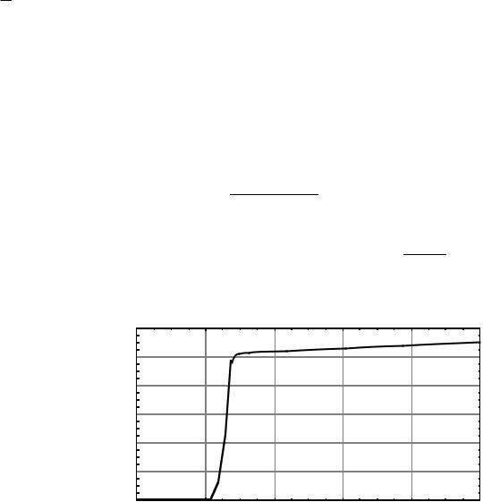
SPICE Results: |
|
|
|
|
|
|
|
|
|
|
|
|
|
120 A |
|
|
|
|
|
|
|
|
|
|
|
|
100 A |
|
|
|
|
|
|
|
|
|
|
|
|
80 A |
|
|
IOUT ≈ 2.8 A for |
VDD 4V →6V |
|
||||||
|
|
|
|
|
|
|
|
|
|
|
||
|
60 A |
|
|
|
|
|
|
|
|
|
|
|
IOUT |
|
|
|
|
|
|
|
|
|
|
|
|
|
40 A |
|
|
|
|
|
|
|
|
|
|
|
|
20 A |
|
|
|
|
|
|
|
|
|
|
|
|
|
0 A |
|
|
|
|
|
|
|
|
|
|
|
|
0V |
2V |
|
4V |
6V |
|
8V |
|
|
10V |
|
|
|
|
|
|
|
VDD |
|
|
|
|
|
|
Allen and Holberg - CMOS Analog Circuit Design |
Page V.5-10 |
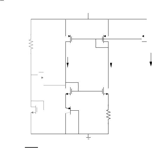
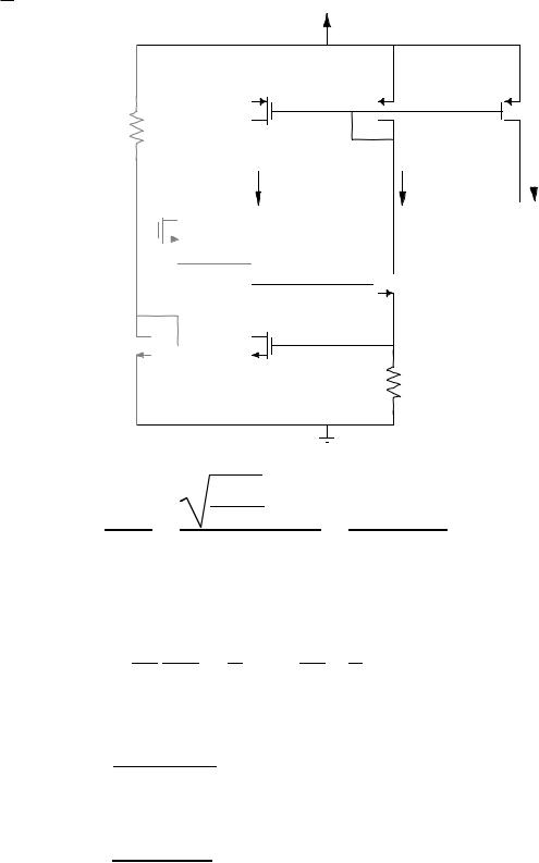
Base-Emitter Voltage Referenced Circuit
 VDD
VDD
|
|
M4 |
RB |
M3 |
M5 |
|
|
|
|
ID1 = I1 |
iOUT |
|
ID2 = I2 |
|
|
M6 |
|
|
M1 |
M2 |
M8 |
Q1 |
R |
|
|
I |
2 |
≈ VBE1 |
= I |
5 |
|
R |
|
V = I2R ≈ VBE1
Allen and Holberg - CMOS Analog Circuit Design Page V.5-11
V.5-2 - TEMPERATURE DEPENDENCE
Objective
Minimize the fractional temperature coefficient which is defined as
|
|
TCF = |
1 |
∂Vref |
parts per million per |
°C or ppm/°C |
|
||||||||||
|
|
|
|
∂T |
|
|
|||||||||||
|
|
|
|
Vref |
|
|
|
|
|
|
|
|
|
|
|
||
Temperature Variation of References |
|
|
|
|
|
|
|
|
|||||||||
PN Junction: |
|
v |
|
|
|
|
|
|
|
|
|
|
|
|
|||
|
|
|
|
|
|
|
|
|
|
|
|
|
|
|
|||
|
i ≈ Isexp |
|
|
∂I |
|
∂(ln I |
) |
|
V |
|
V |
|
|||||
|
|
|
|
Vt |
|
|
|
3 + |
GO ≈ |
|
|||||||
|
|
|
|
-V |
|
|
1 s |
= |
s |
= |
|
|
GO |
||||
I = KT3 exp |
GO |
|
Is ∂T |
|
∂T |
|
T |
TVt |
TVt |
||||||||
s |
|
|
|
|
|
|
|
|
|
|
|
|
|
|
|
|
|
|
|
|
|
Vt |
|
|
|
|
|
|
|
|
|
|
|
|
|
|
|
|
|
|
|
|
|
|
|
|
|
|
|
||||
dvBE |
≈ |
V BE - VG O |
= -2mV/°C at room temperature |
|
|
|
|||||||||||
dT |
|
T |
|
|
|
|
|
||||||||||
|
|
|
|
|
|
|
|
|
|
|
|
|
|
|
|||
= 1.205 V and is called the bandgap voltage)
Gate-Source Voltage with constant current (Strong Inversion):
dVGS |
dVT |
|
2L |
|
|
|
d |
ID |
|||
dT |
= dT |
+ |
WC |
dT |
µ |
|
|
|
ox |
|
o |
µo = KT-1.5 |
; VT = VT0 - αT |
or VT(T) = VT(To) - α(T-To) |
||
dVG S |
|
3 V GS - VT |
||
dT = - α + |
|
T |
|
|
4 |
|
|||


 I
I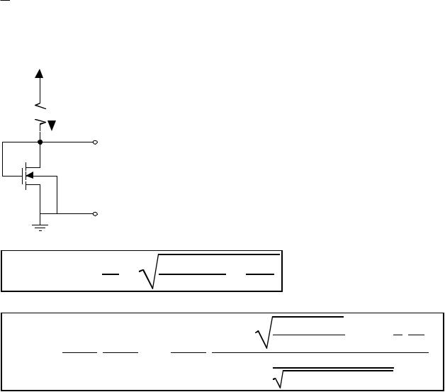
Allen and Holberg - CMOS Analog Circuit Design |
Page V.5-13 |
Gate - Source Referenced Circuits
MOS Equivalent of the PN Junction Referenced Circuit
VDD
R 
 I
I
+
VREF
-
|
|
|
1 |
|
2(VDD−VT) |
|
1 |
|
|
|
|
|
V R E F = V T − βR + |
|
βR |
|
+ |
β2R2 |
|
|
|
|
|||
|
|
|
|
|
|
|
|
|
VDD − VR E F 1.5 |
|
1 d R |
|
T C F |
= |
1 |
dVR E F |
= |
1 |
− α + |
2βR |
T |
− |
R dT |
||
VREF |
dT |
VREF |
|
|
1 + |
|
1 |
|
|
|||
|
|
|
|
|
|
|
|
|||||
|
|
|
|
|
|
|
|
|
2βR (VDD − VREF) |
|
||

Allen and Holberg - CMOS Analog Circuit Design Page V.5-14
Example
W = 2L, VDD = 5V, R = 100 KΩ , K’=110 µ, VT = 0.7, T = 300 K, α = 2.3
mV/°C
Solving for VREF gives
VREF = 1.281 V
RdTdR = +1500 ppm/°C
|
|
|
|
-3 |
|
5 − 1.281 |
|
1.5 |
|
|
-6 |
|||
|
1 |
dVREF |
|
−2.3 ×10 |
+ |
|
|
-6 |
× 100K |
300 |
− 1500 |
× 10 |
|
|
TCF = |
= |
1 |
|
2 × 2 110×10 |
|
|
|
|
|
|
||||
1.281 |
dT |
1.281 |
1 |
+ |
|
|
1 |
|
|
|
|
|
||
|
|
|
|
|
|
|
|
|
|
|
|
|
||
|
|
|
|
|
|
|
-6 |
|
|
|
|
|
|
|
|
|
|
|
|
|
2 × 2 110×10 |
|
|
× 100K (5 - 1.281) |
|
|
|||
TCF = - 928 ppm/°C
Allen and Holberg - CMOS Analog Circuit Design Page V.5-15
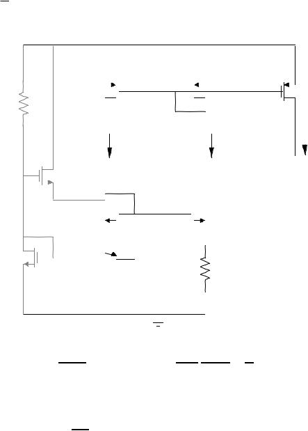
Bootstrapped Current Source/Sink
|
|
VDD |
|
|
M4 |
RB |
M3 |
M5 |
|
ID1 = I1 |
iOUT |
|
ID2 = I2 |
|
|
M6 |
|
|
|
M2 |
M8  M1
M1
R
|
|
2ID1L |
|
|
|
|
VGS1 |
|
K'W |
+ V T |
|
VON + VT |
|
ID2 = R |
= |
R |
|
= |
R |
= ID1 = IOUT |
Assuming that VON is constant as a function of temperature because of the bootstrapped current reference, then
|
TC |
F |
= |
1 |
dVT |
- |
1 dR |
= |
-α |
- |
1 dR |
||
|
VT dT |
R dT |
VT |
R dT |
|||||||||
|
|
|
|
|
|
|
|
||||||
|
|
|
|
|
|
|
|
|
|||||
If |
R is a polysilicon resistor, then |
|
|
|
|||||||||
|
TC |
F |
= |
-2.3 x 10⁻³ |
|
- 1.5x10-3 = -3800 ppm/°C |
|||||||
|
|
|
1 |
|
|||||||||
|
|
|
|
|
|
|
|
|
|
|
|
||
If |
R is an implanted resistor, then |
|
|
|
|||||||||
|
TC |
F |
= |
-2.3 x 10⁻³ |
|
- 0.4x10-3 = -2700 ppm/°C |
|||||||
|
|
|
1 |
|
|||||||||
|
|
|
|
|
|
|
|
|
|
|
|
||
Allen and Holberg - CMOS Analog Circuit Design |
Page V.5-16 |
Base-Emitter Voltage - Referenced Circuit
 VDD
VDD
|
|
M4 |
RB |
M3 |
M5 |
|
|
|
|
ID1 = I1 |
iOUT |
|
ID2 = I2 |
|
|
M6 |
|
|
M1 |
M2 |
M8 |
Q1 |
R |
|
|
I |
2 |
≈ |
vBE1 |
-----> TC |
F |
= |
1 |
dvBE |
- |
1 dR |
|
R |
vBE |
dT |
R dT |
||||||||
|
|
|
|
|
|||||||
|
|
|
|
|
|
|
Assuming VBE = 0.6 volts and a polysilicon resistor gives TCF = 0.61 (-2x10⁻³) - (1.5x10⁻³) = -4833 ppm/°C